JOURNAL OF NANO- AND ELECTRONIC PHYSICS А А - А
Vol. 6 No 3, 03020(4pp) (2014) Том 6 № 3, 03020(4cc) (2014)
The article was reported at the International Conference «The Advanced Technology, Equipment and Analytical Systems for Materials», Kursk, 13-14 May, 2014
2077-6772/2014/6(3)03020(4) 03020-1 2014 Sumy State University
Monolithic Silicon Photodetector - Detector of Ionizing Radiation Based on Functional
Integrated MOS Structures
S.A. Legotin, V.N. Murashev, S.I. Didenko, O.I. Rabinovich, D.S. Elnikov, A.A. Krasnov,
M.A. Bazalevsky, G.I. Koltsov, K.A. Kuzmina
NIST “Moscow Institute of Steel and Alloys”, 4, Leninskiy Pr., 119040 Moscow, Russian Federation
(Received 19 May 2014; published online 15 July 2014)
This paper describes the principle of operation, construction, architecture and fabrication of a new type of monolithic silicon coordinate photodetector - detector of optical and ionizing radiation (MSCP) on the basis of functional integrated MOS structures. The analytical estimation of electrophysical characteristics MSCP is given. It is shown that MSCP is a specialized monolithic silicon VLSI containing two-dimensional pixel array with high and low voltage functionally integrated structures (FIS) and peripheral electronic circuits of amplification and signal processing matrix. Estimations and presents comparative characteristics are presented. They show potential MSCP possibilities for registration of optical and ionizing radiation. Experimental results of -particles and electrons registration. The possible areas of application, with the possibility of its use in a wide X-ray panels medical supplies, X-X-rays, etc are considered.
Keywords: Monolithic silicon coordinate photodetector, Functionally integrated structure, X-rays, Registration of optical and ionizing radiation.
PACS numbers: 42.79.Pw, 85.60.Gz
1. INTRODUCTION
Registration and more high-quality images of objects in the flow of optical and ionizing radiation are essential for a wide range of scientific and applied problems [1]. It leads to an interest in the development of new types of coordinate detectors and photodetectors (CDP) with a radically better performance [2, 3].
Currently, in addition to conventional X-ray film, it is widely used types of new detectors, shown in Table 1, which are divided into two groups: quantum digital (CDC) and analog (QAD) detectors [4].
They have radically different principle of action, namel, the CDP recorded individual photons incident on the pixel, and QAD recorded average value of the energy incident on the pixel matrix CDP.
At his moment mainly popular are strip coordinate detectors [5], which are the simplest build semiconductor devices based on p-i-n diodes. But during using them it needs special electronics.
At the same time leakage of amplifier properties in p-i-n diodes strictly limit their speed and possibility of double (triple) coordinate investigation, at the same time connecting special external electronics to rows and columns makes this very expensive and huge.
By the way the solving of such problems is developing hybrid detector integrated circuit [6-10], produced by flip-chip technology. In this technology direct connection pixels of different chips (register and scan) are: first receive irradiation which contains detective pixels, and second pixels which have amplifier properties and signal properties.
Flip-chip technology leads to determine detectors of high quality which corresponds to X-ray panels for medical equipments.
But current technology has some disadvantages-high prices, and complicated technology process of detectors as it is need to have in one X-ray panel about 2 thousand megapixel chips at the same time they are need to ne directly connections for millions of pixels of register and
analysis chips. Further increasing quality due to reducing pixels sizes lead to more complicated structure.
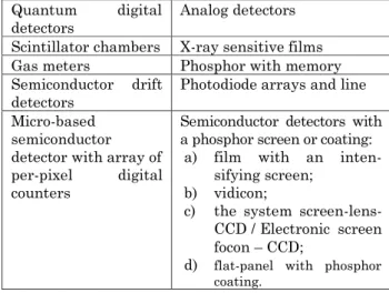
Table 1 –Device examples
Quantum digital detectors
Analog detectors
Scintillator chambers X-ray sensitive films
Gas meters Phosphor with memory
Semiconductor drift detectors
Photodiode arrays and line
Micro-based semiconductor detector with array of per-pixel digital counters
Semiconductor detectors with a phosphor screen or coating:
a) film with an inten-sifying screen;
b) vidicon;
c) the system screen-lens-CCD / Electronic screen focon – CCD;
d) flat-panel with phosphor coating.
Thus both types of detectors have fundamental limitations on the effectiveness of the registration, namely, CDP limited by maximum intensity (power) of the photon flux, which they manage to register for a specific time. QAD are limited by an error converting the analog signal into digital code, different energy photons and limited cycle time of registration – identification the signal and, therefore, they have limited performance [11-14].
In this regard, QDDs are increasingly used during registration of low-intensity radiation to 1010 photon /
(cm2s) used in mammography, crystallography, etc., and
QAD is used for high intensity radiation more than 1010 photon / (cm2s) used in radiography, tomography,
S.A. LEGOTIN,V.N. MURASHEV, ET AL. J. NANO- ELECTRON. PHYS. 6, 03020 (2014)
03020-2
2. EXPERIMENTAL PROCEDURES
MSCP design proposed by the authors in [5]. Figure 1 shows the basic structure of the fragment MSCP pixels, and its circuitry in Fig. 2.
Fig. 1 – FIS pixels MSCP
Figure 1 shows that MCSP be used as a coordinate photodetector of optical radiation, a direct detector with direct conversation energy ionizing rays or indirectly there is the scintillator on the surface. Each absorbed high-energy photon generates a charge in the silicon substrate electron-hole pairs Qz. They are separated by an electric field Ef in the space charge region (SCR), creating an ionization current Iion in SCR PIN diode that passing through the resistor generates a voltage pulse Uinacross the resistor and it is amplified by MOS transistor (Fig. 2).
Fig. 2 – Schematic diagram of the detector pixels redraw transistor IC pixels MSCP
Figure 1 shows that the pixels detector is a single FIS containing in a lightly doped substrate recording high-voltage PIN diode and low-voltage n-MOS transistor with built-in channel. It is important that the electron-hole pairs are collected (ionization current is produced), namely by p+ +-n-p junction of PIN diode
having a lower potential on the p++- region than the p
k region containing.
MSCP represents specialized monolithic silicon VLSI containing, recording two-dimensional matrix with high voltage PIN diode and low-voltage n-MOS transistors and low-voltage peripheral CMOS circuitry amplification and signal processing pixel detector.
2.1 Analytical Evaluation of the Electrical Characteristics of MSCP Pixels
2
0 , 2
D D
q N W
U (1)
where UD UDD+ Ub ; UDD – the supply voltage; Ub – the bias voltage of ++-area of PIN diode; q– the elementary
charge; ND –donor concentration; W– the width of space charge region; ε – electric permittivity; ε0 – relative
permittivity.
Impurity concentration on high resistance substrate is 1012сm– 3. Collecting time of electron (t
e) and holes (th) could be calculated respectively [6]:
2
2
ln 1 ,
2
D abs D
e
n D D D
U U d L U
d t
U U U d U U (2)
2
2
ln 1 ,
2
abs D
h
p D D
L U
d t
U d U U (3)
where d– the detector thickness; n– electron mobility, μp –hole mobility; UD– the minimum voltage needed for full depletion; U – the applied voltage; Labs – the absorption length.
The electron mobility in the high-resistivity silicon having a resistivity of 5 Ohm∙cm up to 1100 cm2V– 1s– 1.
Drift time tdr depends on absorption depth of ionizing particle in the silicon. In Table 2 the particle energy, absorption depth for different types of ionization sources are shown.
The amplitude of the ionization current Iion, is given by:
,
1 1
,
ion n p
e h
I q N
t t (4)
where q– the elementary charge, Nn,p.– the number of
electron-hole pairs generated by incident radiation; te– the electron collecting time; th– the hole collecting time.
3. RESULTS AND DISCUSSION
At first the Indium concentration influence on the nonideality factor (n) vs. the current density reveals the following (Fig. 1).
The magnitude of the input signal Uin can be estimated from:
,
in ion
U I Z (5)
where Iion – the ionization current; Z – the input impedance circuit pixels.
1
1 1
,
C G
Z
X R (6)
where Z– the input impedance circuit pixels; XC– the reactive resistance; RG– the gate resistance.
The reactive resistance ceated by total capacity of PIN diode Cpin and gate of MOS transistor G:
1
, 2
C
pin G
X
f C C (7)
where f 1 / tshift.
MONOLITHIC SILICON PHOTODETECTOR-DETECTOR… J. NANO- ELECTRON. PHYS. 6, 03020 (2014)
03020-3 Table 2 – The features of common ionization sources
Radiation type
Energy, eV
Absorption depth, mkm
Drift time, ns
Exiton quantity
Optical
quant 1,1 1 ~ 0,5 1
X-ray photon from Fe55
5,9103 30 ~ 3 1600
α–particle 5106 25 ~ 4 3105
Taking into account that that the capacitance Cs210– 15 F/mkm2 for a typical MOS transistor with a channel length Lch 1 mkm and a width Wc 1 mkm, the capacitance PIN diode Cpin 0,510– 15 F/mkm2 for the pixels of 100 100 micrometers.
Table 3 –The ionization current and the input signal for different types of influence
Radiation type Ionization current Iion, nA
Input voltage Uin, mV
Optical quant 0,3 7,5∙10– 3
X-ray photon from
Fe55 source 85 10
α – particle 1,2∙104 1800
The output value is equal:
,
out U in
U K U (8)
where Uout – the output signal; KU – gain MOSFET typically equal to 10; Uin– the input signal.
The time constant τ of the input circuit recharge pixels can be determined from the expression:
cCoutRG, (9)
where Cout– the capacitance of the output circuit; RG– the gate resistance.
Then pixels performance power is:
pdrc, (10)
where τdr – the drift time of charge carriers. Calculation results for performance listed in Table 4.
Table 4 – The operation speed and the output signal for different types of influence
Radiation type Output signal, V Speed τp, ns
Optical quant 7510– 6 2,5
X-ray photon from
Fe55 0,1 5
– particle 18 6
3.1 Architecture, Topology and Fabrication of MSCP
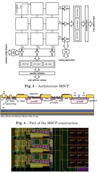
Figure 3 shows the MSCP architecture (block diagram), which works as follows: in the pixel ingress of ionizing particles causes the source and drain currents which are applied to the respective coordinate lines of the matrix X and Y, where they are amplified linearly to form the output signal Uout is proportional to the
particles energy and the time of its occurrence, and the addresses of the coordinate lines is encoded in binary code encoder.
MSCP is VLSI containing recording two-dimensional array of active functionally integrated MOS structures and peripheral n-MOS circuitry amplification and signal processing coming from the matrix as a result of the effects of ionizing particles.
This detector allows you to get full information about each individual particle, namely, to define two (or three) of its coordinates, time of arrival and the absorbed energy of the particle.
Manufacturing technology of such a detector uses standard processes used in the creation of modern silicon CMOS chips. The starting material was in high-resistivity n-silicon plates with sided polishing orientation 111. Plate thickness (different samples) 300-500 microns in diameter 100 mm. Resistivity silicon ρn 5-10 kOm cm, respectively, the concentration of the dopant n-impurity Nc21011 cm– 3; minority carrier lifetime (ingot ) 2 ms. At all stages of the formation of active regions ion implantation was used. More detail manufacturing process is considered in [7]. VLSI chip design fragment is shown in Fig. 4, and its topology in Fig. 5.
Fig. 3 – Architecture MSCP
Fig. 4 – Part of the MSCP construction
S.A. LEGOTIN,V.N. MURASHEV, ET AL. J. NANO- ELECTRON. PHYS. 6, 03020 (2014)
03020-4
4. EXPERIMENTAL RESULTS
During this work experimental investigation of spectral (detecting -particles, electrons) MAPS characteristics was developed. As it is shown in [17] silicon slow interacts with -irradiation, that is why investigation was not made.
-particle spectrum of 239Pu (5.15 MeV) obtained for
MAPS samples is shown in Fig. 6.
Fig. 6 –-particle spectrum of 239Pu (5, 15 MeV)
Fig. 7 –Electron spectrum of 207Bi (mean energy Ee 1 MeV)
Spectral resolution of the investigated detector for α-particles was 11.2 % and corresponds to the resolution of typical strip detectors. The peak expansion from the low-energy side is equal to 8.2 %,
and from the high-energy part – 3 %. This asymmetry of the peak in the low-energy part of the spectrum is probably caused by contribution of the diffusion current of generated charge carriers.
Single-charged relativistic particles spectra are shown in Fig. 7. These particles were electrons from the
-sources of 207Bi.
5. SUMMARY
A new type of MSCP is a specialized VLSI, containing recording pixel matrix functionally – integrated structures and peripheral circuits amplification and signal coding ionizing particles;
the estimates and comparative characteristics show potential MSCP possibilities for registration of optical and ionizing radiation;
architecture MSCP was designed;
MSCP topology was developed;
it is shown that MSCP can be manufactured by conventional CMOS technology, and may be directly, without intermediate electronic circuits combined with the computer;
experimental investigations and estimates have shown the possibility of a high quality registration MSCP different types of radiation, in particular
-particles and electrons with coordinate accuracy
not less than 20 microns, with a time resolution better than 20 ns and a spectral resolution not less than 10 %;
it is shown that MSCP can be applied in various devices in nuclear physics, medical devices and customs control.
AKNOWLEDGEMENTS
This study was supported by the Federal Targeted Program “The development of electronic component base and radio electronics” for 2008-2015, state contract №14.430.12.0001.
REFERENCES
1. G.I. Koltsov, S.I. Didenko, A.V. Chernykh, S.V. Chernykh, A.P. Chubenko, Yu.N. Sveshnikov, Semiconductors46 No 8, 1066 (2012).
2. D.L. Volkov, D.E. Karmanov, V.N. Murashev, S.A. Legotin, R.A. Mukhamedshin, A.P. Chubenko, Instruments and
Experimental Techniques52 No 5, 655 (2009).
3. V.N. Murashev, S.A. Legotin, O.M. Orlov, A.S. Korol'chenko, P.A. Ivshin, Instruments and Experimental Techniques 53
No 5, 657 (2010).
4. F.M. Baryshnikov, G.I. Вritvich, A.V. Chernykh, S.V. Chernykh, A.Р. Chubenko, S.I. Didenko, G.I. Koltsov, AIP Conference Proceedings Ion Implantation Technology 2012: 19th International Conference on Ion Implantation Technology, 1496, 50 (2012).
5. V.N. Murashov, S.A. Legotin, V.A. Ryabov. Patent of Russia
№ 2494497 at 21.07.2011.
6. G. Lutz, Semiconductor Radiation Detectors (2007).
7. V.N. Murashev, S.A. Legotin, D.E. Karmanov, F.M. Baryshnikov, S.I. Didenko, J. Alloy. Compd.586, S553
(2014).
8. S.P. Beaumont, et al., NIM A172, 321 (1992). 9. W. Kucewicz, et al., Acta Phys. Pol. B30, 2075 (1999). 10. M. Amati, et al., Nucl. Instrum. Methods A511, 265 (2003). 11. O. Ehrmann, Private communication (Berlin: 2004). 12. L. Andricek, Radiation hardness of DEPFET detectors.
(Presented at the 2005 International Linear Collider Workshop: Stanford: March 18-25, 2005).
13. M. Amati, et al., Nucl. Instrum. Meth.A511, 265 (2003). 14. Y. Araia, et al., Development of a CMOS SOI Pixel Detector.
SLAC-PUB-13374 (2008).
15. L. Rossi, P. Fischer, T. Rohe, N. Wermes, Pixel Detectors From Fundamentals to Applications (Berlin: Heidelberg: New York: Springer: 2006).
16. G. Lutz, Semiconductor Radiation Detectors. Device Physics (Berlin- Heidelberg: Springer: 1999).