Jaime Leandro Lino Teyller
Licenciado em Ciências da Engenharia Electrotécnica e de Computadores
Contribution for the Optimization of the Design
and Manufacture of Low-Resistance
Short-Circuited Superconducting Coils
Dissertação para obtenção do Grau de Mestre em Engenharia Electrotécnica e de Computadores
Orientadora: Doutora Anabela Monteiro Gonçalves Pronto, Professor Auxiliar,
FCT, Universidade NOVA de Lisboa, Portugal Co-orientador: Doutor João Miguel Murta Pina,
Professor Auxiliar,
FCT, Universidade NOVA de Lisboa, Portugal
Júri Presidente: Doutor Rui Neves-Silva
Arguente: Doutor Mário Ventim Neves
Contribution for the Optimization of the Design and Manufacture of Low-Resistance Short-Circuited Superconducting Coils
Copyright © Jaime Leandro Lino Teyller, Faculdade de Ciências e Tecnologia, Universi-dade NOVA de Lisboa.
The Faculdade de Ciências e Tecnologia and the Universidade NOVA de Lisboa have the right, perpetual and without geographical boundaries, to file and publish this dissertation through printed copies reproduced on paper or on digital form, or by any other means known or that may be invented, and to disseminate through scientific repositories and admit its copying and distribution for non-commercial, educational or research purposes, as long as credit is given to the author and editor.
To the memory of my Father. To my mother and to my Aunt.
Acknowledgements
To the Department of Electrical Engineering of the Faculdade de Ciências e Tecnolo-gia, Universidade NOVA de Lisboa, for the necessary support of this work,
To my Advisers, Professors Anabela Pronto and João Murta Pina, the warmest recog-nition and gratitude for all the patience, guidance, counselling and constant readiness. It really was a pleasure,
To my Professors at the Department of Electrical Engineering and other departments of the faculty along this journey, under penalty of forgetting someone. All contributed to my knowledge and here goes my special acknowledge,
To 4x4 Multitrabalhos in the person of Daniel Domingues for accepting the challenge to cut the tapes by water jet and to ITEP/KIT in the person of Drs. Wescley de Sousa and Anna Kario for cutting the tapes by the punching method,
To Professor Christopher Auretta for all the brownies and friendship that certainly sweetened this journey and Dra. Maria do Rosário Duarte for all the patience and support, To my colleagues for the support during the course, especially to Adriana Mar, Carla Borges and Nuno Vilhena for the inputs during the present work,
To my family and friends for the constant comprehension of my absence. And espe-cially to Luana Boavida, Nádia Marques, Dário Teca, Inalinda Fonseca, Carla Martins, Jandira Almeida, Helton Trindade, Kwame Almeida, Darcy Viera Lopes, Claudia Videira, my aunt Sofia Teyller and my mother Cristina Lino for all the support on every hour.
Abstract
The present dissertation intends to contribute to the optimization process of the de-sign and manufacture of low-resistance short-circuited superconducting coils in an archi-tecture developed in Department of Electrical Engineering of Faculdade de Ciências e Tecnologia (DEE-FCT) of the Universidade NOVA de Lisboa.
The design optimization of the previously proposed coil architecture is carried out in this work. After validation of the new design, the superconducting tapes are cut through two different methods, i.e. by water jet and punching. The critical current of the tapes is measured to assess the quality of the cut made and the preservation of the superconduct-ing properties of the tapes.
The most suitable method to perform the joint of the coils is determined by measur-ing the contact resistance at the joints usmeasur-ing different solder materials and configurations. Prototypes of coils with 4 and 8 turns are constructed, and an experimental test for the determination of the critical currents through the induction of superconducting currents into the coils is carried out.
It is concluded that the water jet is very aggressive to cut the tapes and difficult to adapt to large tape lengths using the current conventional machines. It is verified a better aptitude of the punching method through a cutting machine adaptable to the various moulds and lengths, conditioned by the fact that it is currently a restricted access process. Some suggestions are made for future works which do not exhaust in this dissertation.
Keywords: High-Temperature Superconductors; Coated Conductors; Short-Circuited Coils; Low-Resistance Joints; Critical Current Density.
Resumo
A presente dissertação pretende dar um contributo ao processo de otimização inerente ao projeto e fabrico de bobinas supercondutoras em curto-circuito e baixa resistência, numa arquitetura desenvolvida no Engenharia Electrotécnica e de Computadores da Fa-culdade de Ciências e Tecnologia (DEE-FCT) da Universidade NOVA de Lisboa.
Realiza-se neste trabalho a otimização do design da arquitetura de bobinas anterior-mente proposta. Após validação do novo design, procede-se ao corte das fitas supercondu-toras através de dois métodos distintos, ou seja, por jato de água epunching. Determina-se
a corrente crítica das fitas para aferir a qualidade do corte efetuado e a preservação das propriedades supercondutoras das fitas.
O método mais adequado à realização da junção das bobinas é determinado através da medição da resistência de contacto nas junções utilizando diferentes materiais de soldadura e configurações. Constroem-se protótipos com 4 e 8 espiras ensaiam-se expe-rimentalmente para determinação da corrente crítica através da indução de correntes supercondutoras nas bobinas.
Conclui-se que o jato de água é bastante agressivo para o corte das fitas e de difí-cil adaptação para grandes comprimentos de fita utilizando as máquinas convencionais atuais. Verifica-se uma melhor aptidão do método de corte porpunching através de uma
máquina de corte adaptável aos vários moldes e comprimentos, com a ressalva de atual-mente ser um processo de acesso restrito.
Efetuam-se algumas sugestões para trabalhos futuros que não se esgotam na presente dissertação.
Palavras-chave: Supercondutores de Alta Temperatura; Condutores Revestidos; Bobinas de Curto-Circuito; Junções de Baixa Resistência; Densidade de Corrente Crítica.
Contents
List of Figures xv
List of Tables xvii
Acronyms xix 1 Introduction 1 1.1 Motivation . . . 1 1.2 Research Objectives . . . 2 1.3 Original Contributions . . . 2 1.4 Thesis Structure . . . 2 2 Literature Review 5 2.1 Superconductors, a Brief Introduction . . . 5
2.2 High-Temperature Superconducting Materials. . . 7
2.2.1 Available Commercial Forms . . . 9
2.2.2 Applications of HTS Materials. . . 12
2.3 Coated Conductors . . . 13
2.3.1 Manufacturing Process . . . 13
2.3.2 Coated Conductors Constraints . . . 16
2.4 Coils from Coated Conductors . . . 17
2.4.1 Winding Processes . . . 18
2.4.2 Cutting Methods . . . 20
2.4.3 Junction Methods . . . 22
2.4.4 Applications of HTS Coils . . . 26
2.5 Synopsis . . . 28
3 Analysis of the Tapes Cutting Process 29 3.1 Design of the HTS Coils. . . 29
3.2 Cut of the Tapes . . . 32
3.2.1 Cut of the Tapes by an Electrician Scissor . . . 32
3.2.2 Cut of the Tapes by Water jet Method . . . 32
3.2.3 Cut of the Tapes by Punching Method . . . 36
C O N T E N T S
3.3.1 Critical Current after Water Jet Cut . . . 41
3.3.2 Critical Current after Punching Cut. . . 46
3.3.3 Comparison of the Cut Methods. . . 47
3.4 Synopsis . . . 47
4 Analysis of Joining Process 49 4.1 Experimental Procedure for the joints. . . 49
4.2 Determination of the joining method . . . 50
4.3 Synopsis . . . 54
5 Development of Prototype Coils 55 5.1 Design of the HTS Coils. . . 55
5.2 Developed Prototypes. . . 56
5.3 Experimental Procedure . . . 57
5.4 Experimental Results and Analysis of the Prototypes . . . 60
5.5 Synopsis . . . 65
6 Conclusions and Future Work 67 6.1 Conclusions . . . 67
6.2 Future Work . . . 68
Bibliography 69
List of Figures
2.1 Generic phase diagram (T-J-H) of a superconductor . . . 6
2.2 Timeline of some known superconductors . . . 9
2.3 Seeded melt growth bulk from YBCO material . . . 9
2.4 A schematic outline of the PIT process . . . 10
2.5 Cross-section of a Bi-2212 multifilamentary round wire . . . 11
2.6 Cross-section of a 1G tape manufactured using Bi-2212 material . . . 11
2.7 Generic schematic of a layered architecture for a Coated Conductor . . . 12
2.8 A summarizing schematic of manufacturing methods for 2G CC . . . 14
2.9 Different types of strain and mechanical strength on a Coated Conductor . . 16
2.10 Short-circuited DP wound with NI winding technique . . . 18
2.11 A low-resistance HTS short-circuited coil using the LW technique . . . 19
2.12 Jointless continuous HTS coils . . . 19
2.13 Fabrication of Roeble cables by the mechanical punching technique . . . 21
2.14 Main types of joint configurations used . . . 23
2.15 Sketch of bridge joint variants . . . 24
2.16 Different kind of soldering devices used to make joints . . . 25
2.17 Electrical diagram of an iSFCL . . . 27
2.18 No-Insulated coil made of CC for the secondary of an air core iSFCL . . . 28
3.1 Required procedures to implement a short-circuited low-resistance coil with multiple turns . . . 30
3.2 Design of the proposed coil geometry . . . 31
3.3 A water jet cutting head used in the process to cut the tapes . . . 33
3.4 A tape sandwiched between the acrylic and wood materials . . . 33
3.5 Three tape pieces of 400 mm cut in a mixed geometry by water jet . . . 34
3.6 Result of a 1072 mm long piece of tape cut by water jet . . . 35
3.7 The issues on using the water jet cut method. . . 35
3.8 Delamination issues due to the utilization of water jet cut method . . . 36
3.9 An overview of the punching machine used to cut the tapes . . . 36
3.10 Pneumatic adjustable punching tool . . . 37
3.11 A transition section for a 1072 mm tape cut by the punching method . . . . 37
3.12 Considered points for the measurement of Iccurrent on the tapes . . . 38
L i s t o f F i g u r e s
3.14 Rupture of tape due to excessive injected current . . . 40
3.15 Results of Ic critical current for the first of three tested tapes . . . 41
3.16 Results of Ic critical current for the second of three tested tapes. . . 42
3.17 Results of Ic critical current for the third of three tested tapes . . . 42
3.18 Results of Ic critical current for the N4 tape, cut by water jet: The straight sections . . . 43
3.19 Results of Ic2 critical current for the N4 tape cut by water jet, at transition section . . . 44
3.20 Results of Ic critical current for the N8 tape, cut by water jet: The straight sections . . . 45
3.21 Results of Ic2 critical current for the N8 tape cut by water jet, at transition section. . . 45
3.22 Results of Ic critical current for the N4 tape, cut by punching . . . 46
4.1 Measuring example for the contact resistance of the joints by the four-points method . . . 49
4.2 Joints built to determine the contact resistance . . . 50
4.3 Example of a fragile joint when using indium solder material applied directly to electroplated copper . . . 51
4.4 Comparison of different joints built with SnAg solder paste in lap and bridge topology . . . 51
4.5 Comparison of different joints built with SnAg and SnAgCu solder pastes . . 52
4.6 Comparison of different joints by topology . . . 53
5.1 Construction of both coils through the annular mould . . . 56
5.2 Final result of both prototype coils assembled through the mould . . . 57
5.3 Electrical diagram of the assembly process to test the prototypes . . . 58
5.4 Experimental assembly used to measure the currents . . . 59
5.5 The 112 turns air-core coil and the cryogenic support. . . 59
5.6 Two results for the prototype coil with four turns . . . 61
5.7 Results of the tests for the prototype coil with four turns . . . 62
5.8 Result for one point of measure for the prototype coil with eight turns . . . . 63
5.9 Result of the last measure for the prototype coil with eight turns . . . 64
5.10 Results of the tests for the prototype coil with eight turns . . . 64
5.11 Results of the superconducting current in tape for the prototype coil with eight turns . . . 65
List of Tables
2.1 Characteristic data of some cuprate superconductors . . . 8
2.2 Industrial and Energy applications for HTS materials . . . 13
2.3 Fabrication key parameters for CC . . . 15
2.4 Recomended solders compositions by manufacturers, Pb-free . . . 26
3.1 General parameters considered for the design of HTS coils. . . 31
3.2 Considered coil design parameters used for the cut of tapes by an electrician scissor . . . 32
3.3 Calculated design parameters for two tapes, to build coils with four and eight turns . . . 34
3.4 Measured values of critical current for the cut by an electrician scissor . . . . 38
3.5 Summary of Ic critical current measurements for different tapes. . . 47
4.1 Summary of the temperatures and time used to build the linear joints. . . 50
4.2 Summary of the normal resistance values of the joints tested. . . 53
5.1 Specific parameters for the two prototype coils. . . 55
5.2 Soldering time steps to build the joints for both coils.. . . 57
5.3 Tests results for a prototype coil with 4 turns. . . 60
Acronyms
1G first generation.2G second generation.
ABAD Alternating Beam Assisted Deposition.
Bi-2223 Bismuth-Strontium-Calcium-Copper-Oxide, (Bi, Pb)2Sr2Ca2Cu3O10−x. Bi-2212 Bismuth-Strontium-Calcium-Copper-Oxide, Bi2Sr2CaCu2O8+x.
BLCO Barium-Lanthanum-Copper-Oxide, BaLaCuO.
BSCCO Bismuth-Strontium-Calcium-Copper-Oxide, (Bi, Pb)2Sr2Can−1CunO2n+4.
CC Coated Conductors.
DP Pancake or Double-Pancake. EDM Electrical Discharge Machining. EPG Electric Power Grids.
FAIR Facility for Antiproton and Ion Research. HBCCO Mercury-Barium-Calcium-Copper-Oxide. HTS High-Temperature Superconductors.
IBAD Ion Beam Assisted Deposition.
iSFCL Inductive Superconducting Fault Current Limiters. ITER International Thermonuclear Experimental Reactor. KIT Karlsruhe Institute of Technology.
LHC Large Hadron Collider.
LTS Low-Temperature Superconductors. LW Layer-Wound.
AC R O N Y M S
MOCVD Metal-Organic Chemical Vapour Deposition. MOD Metal-Organic Deposition.
MRI Magnetic Resonance Imaging. MTG Melt-Textured Growth. NI No-Insulation.
NMR Nuclear Medical Resonance. PCM Persistent Current Mode. PFM Pulsed Field Magnetization. PIT Powder-in-Tube.
PLD Pulsed Laser Deposition.
RABiTS Rolled Assisted Bi-Axially Textured Substrates. RCE Reactive Co-Evaporation.
REBCO alloy of rare-earth elements with Barium-Copper-Oxide, RE123. rSFCL Resistive Superconducting Fault Current Limiters.
SFCL Superconducting Fault Current Limiters. SMES Superconducting Magnetic Energy Storages.
SQUIDs Superconducting Quantum Interference Devices. TBCCO Thallium-Barium-Calcium-Copper-Oxide.
TSMTG Top-Seeding Melt Texture Growth. WASP Walters Spring.
YBCO Yttrium-Barium-Copper-Oxide. YSZ Yttrium-Stabilized Zirconia.
1
Introduction
The present thesis addresses the design of coils made out of thesecond generation (2G) High-Temperature Superconductors (HTS)materials, namely from Yttrium-Barium-Copper-Oxide (YBCO)compound. Furthermore, the unavoidable points of losses intro-duced when considering a low-resistance non-superconducting joints approach.
These coils are intended to be used in practical applications such as Superconduct-ing Fault Current Limiters (SFCL), and possibly in Superconducting Magnetic Energy Storages (SMES)devices and other energy systems or devices where it could fit.
1.1
Motivation
Coils and its design are fundamental for power applications, and when built from superconducting materials presents a series of advantages that can not be suppressed by conventional conductors, in spite of the great challenges that the use of these materials present due to its specific characteristics, and the cryogenic part essential for the opera-tion in the superconducting state.
Amongst other technologies that use HTS coils, inductive SFCL which are charac-terised by the magnetic linkage between the primary and the secondary, require the latter to be short-circuited in order to be able to operate.
The technology underlying theSFCLprojects is currently widespread, and its viability is directly related to the superconducting materials used in the process. Nevertheless, the superconducting tapes are a viable option due to its characteristics in the handling pro-cess, and with the particularity that it can now be produced in lengths of great extension and with few restrictions through processes even more mature.
There are available on the market a wide range of superconducting tapes sold in standard formats, which opens up good prospects for the optimisation of the design of low-resistance, short-circuited, superconducting coils through architectures not tested until now serving as a motto for the present dissertation. Furthermore, theHTScoils can also be used inSMESenergy systems, another promising practical application.
C H A P T E R 1 . I N T R O D U C T I O N
1.2
Research Objectives
This dissertation aims to optimize aspects of the design and manufacture of short-circuited superconducting coils, in an architecture developed at the Department of Elec-trical Engineering of Faculdade de Ciências e Tecnologia (DEE-FCT) of the Universidade Nova de Lisboa. The specific objectives:
i. Superconducting tapes cutting and design of its geometric characteristics; ii. Determination of the best soldering process for the joining process of the coils; iii. Implementation and test of the prototype coils at real-scale dimensions with high
number of turns.
1.3
Original Contributions
Design optimization of a low-resistance short-circuitedHTScoil architecture built by commercially available2Gtape, with several numbers of turns and single joint point.
1.4
Thesis Structure
The dissertation is divided into 6 chapters.
This initial chapter, Introduction, summarizes the proposed work, the motivation that led to its development, the objectives to be achieved, the resulting contributions and the organization of this document.
In the second chapter, the Literature Review is presented bibliographical research of what exists until the present date directly related to the subject of this dissertation. Among the highlights, a brief introduction on superconductivity topic is presented, su-perconductors and main properties as well,HTSmaterials, superconducting tapes and finally coils ofHTSmaterial, the central subject of this thesis.
The third chapter, Analysis of the Tapes Cutting Process, describes the required steps for the prototype development from the design of theHTScoils, the cut of the tapes describing the cut methods, the determination of critical current of the tapes after the cut, ceasing with a comparison of the obtained results.
The fourth chapter, Analysis of Joining Process, describes the experimental proce-dures to join the tapes, the determination of the best join method and solder material to use.
1 . 4 . T H E S I S S T R U C T U R E
The fifth chapter, Development of Prototype Coils, describes the specific parameters considered for the design of the prototype coils, present the developed prototypes, de-scribe the experimental procedure to measure the induced currents into the prototype coils, finalizing with the presentation of the experimental results and analysis of the de-veloped prototype coils.
The sixth and final chapter, Conclusions and Future Work, presents the project’s conclusions, positive and negative aspects of the proposed architecture, and appoints some of the work that does not fall within the scope of the present project and for its relevance can be developed in the future.
2
Literature Review
This chapter addresses some relevant bibliographic concepts to understand the present work. Hence, brief notions about superconducting materials, especially those of theHTS type, development and applications with particular interest forHTScoils are exposed.
2.1
Superconductors, a Brief Introduction
Demand over the years for excellent conducting materials has provided enormous technological advances and appears as one of the prominent areas of research, consid-ering the whole set of applications that may result from it. In this context, continuous search for ideal superconductors is still an objective nowadays.
Liquefaction of gases gave an essential technique to the discovery of a new state of matter, known as the state of superconductivity. For this purpose, contributions such those made in 1823 with CO21by Michael Faraday and in 1898 with H2by James Dewar
(also the inventor of vacuum vessel to store liquid hydrogen six years earlier), paved the way.
Later, in 1908 with liquefaction of He2(a noble gas with the boiling point at
atmo-spheric pressure of 4.2 K), Heike Kamerlingh Onnes extended the available temperature range towards absolute zero (Buckel and Kleiner, 2004; Pina,2010; Saxena,2010). He also reported for the first time superconductivity in 1911, after his investigations of elec-trical properties on metals, such as the mercury in capillary tubes at helium boiling point (Kamerlingh Onnes,1913). From his experiments three important macroscopic results describe the superconductors:
• A sudden vanishing of electrical resistance2on frozen mercury when approaching a temperature point of 4.2 K. This point is designated as the transition or critical temperature, Tc, and all superconductors present the same behaviour;
1Note that, CO
2achieves liquid state at 217 K (above 5.1 atm, not presenting liquid form below this pressure), and H2has the boiling point at 20 K.
2According to Saxena (2010), the resistivity of a superconductor is below 10−27
Ωcm, which compared with an excellent conductor like copper with 10−9Ωcm, can be assumed as zero resistivity (or ideal conduc-tivity) for superconductors.
C H A P T E R 2 . L I T E R AT U R E R E V I E W
• Applying a sufficiently strong magnetic field, known as the critical magnetic field Hc, can destroy the superconducting state, even if below the Tc(Pronto,2010;
Rose-Innes and Rhoderick,1978; Tinkham,1996);
• There is a limit to electrical current density it can support before losing the state of superconductivity, known as the critical current density, Jc(Rose-Innes and Rhod-erick, 1978). Being strongly related to the real temperature of the material and an applied magnetic field, achieving its maximum at absolute zero temperature (Pronto,2010).
These three important results occur due to a remarkable combination of electric and magnetic properties in certain materials when cooled to extremely low temperatures, originating the state of superconductivity, according to Rose-Innes and Rhoderick (1978). Therefore, a well-defined region inside the critical surface defines the boundaries of superconductivity for a superconductor, as illustrated in Figure2.1, whereas outside this region the material is said to be in the normal state.
Figure 2.1: Generic phase diagram (T-J-H) of a superconductor, correlating the physical quantities described above, namely temperature, current density and magnetic field. Adapted from De Marzi et al. (2016).
Superconductors have a distinguished behaviour when in the presence of an applied magnetic field. Hence, are divided into two classes:
• Type I, characterised for being strictly associated withMeissner effect3, in which, an externally applied magnetic field is expelled from within, up to a critical value of Hc, causing loss of superconductivity in the material. This class is mainly comprised of metals and metalloids of a single element4, i.e., mercury, lead and tin (Lehndorff, 2001; Mangin and Kahn,2017; Saxena, 2010), operating with maximum applied fields of 0.1 T, limiting the spectrum of practical applications in power energy field (De Marzi et al.,2016; Pronto,2010).
3A magnetic phenomenon, known as perfect diamagnetism which shows that superconductors are not just perfect conductors, but in fact, repel the magnetic flux from within. For further notes (Pina, 2010; Pronto,2010; Rose-Innes and Rhoderick,1978; Tinkham,1996).
4Note that, transition metals as the widely used niobium or vanadium and technetium are not of type I, but type II instead. An extended list of Type I class can be found at Eck (2018).
2 . 2 . H I G H -T E M P E R AT U R E S U P E R C O N D U C T I N G M AT E R I A L S
• Type II, formed by compounds5 presents a more complex behaviour than type I, with two thresholds Hc1 and Hc2. Meissner effect is exhibited till a specific value
of an applied magnetic field Hc1, a “mixed state” which occurs between Hc1 and
Hc2 values allowing the coexistence of superconducting and normal zones within
the material, and the cease of superconductivity for values above the Hc2threshold.
(Abrikosov,2004; Buckel and Kleiner,2004; Pina,2010; Pronto,2010).
Nevertheless, near the upper critical magnetic field Hc2, higher flux densities are
achieved, i.e., 13 T for Nb-Ti, 23 T for Nb3Sn (Mangin and Kahn,2017), with
transi-tion temperatures Tcabove 10 K for niobium binary compounds (Lehndorff,2001; Saxena,2010), thus, suitable for more practical applications.
2.2
High-Temperature Superconducting Materials
Low cooling temperature of superconducting materials was an important aspect that has restrained many applications over the years, in part, due to the cost of cryogenic materials6and the cooling systems commercial viability. Nevertheless, a milestone was achieved in 1986 withBarium-Lanthanum-Copper-Oxide, BaLaCuO (BLCO)compound by Bednorz and Müller, presenting a transition temperature of 35 K (Bednorz and Müller, 1987). Consequently, introducing the differentiation between Low-Temperature Super-conductors (LTS)and High-Temperature Superconductors (HTS), based on their required transition temperature to exhibit the superconducting properties.
The term"High-Temperature Superconducting" is not consensual since many authors
also use to designate the superconducting materials with transition temperatures be-tween 20 K and 50 K. However, here the term is used for the ceramic superconductors with transition temperatures above the boiling point of liquid nitrogen, i.e., 77 K at at-mospheric pressure, namely, the cuprates in which layers of copper oxide alternate with other elements forming a crystallographic family known as perovskites, essentially ce-ramic materials.
LTSwere widely used for practical applications before the discovery ofHTSand are still important materials nowadays. As an example, type II binary compounds (A-15 or A3B stoichiometry7) are used, presenting transition temperatures above 20 K and upper critical fields above 20 T (Buckel and Kleiner, 2004; Saxena, 2010). And compounds
5A list of type II superconductors constituted by alloys, binary compounds, organic compounds, cuprates (copper oxides), heavy fermions and iron-based superconductors can be found at Eck (2018).
6Amongst several cryogenic materials available, helium, hydrogen and nitrogen with boiling points of 4.2, 20.4 and 77.3 K respectively, are the most widespread, being liquid nitrogen the most cheaper nowadays. 7A stoichiometry constituted by an ‘A’ from the transition metals such as Nb, V, Ta or Zr and ‘B’ metals or semiconductors such as Sn, Al, Ga, Ge, In or Si.
C H A P T E R 2 . L I T E R AT U R E R E V I E W
as Nb-Ti and Nb3Sn widely used for superconducting magnets construction, takes
ad-vantage of the higher upper critical field characteristic of the type II superconductors, presenting current densities above 109 Am−2, i.e., hundred times higher than those ob-tained in copper wires (107Am−2) (De Marzi et al.,2016).
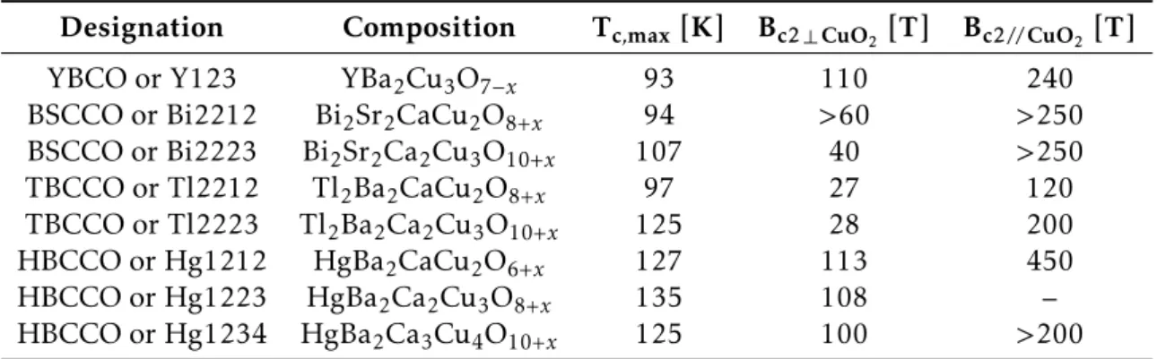
HTSdiscovery provided an all-new set of superconducting materials, although, the most used are based on yttrium variants of YBCO and Bismuth-Strontium-Calcium-Copper-Oxide, (Bi, Pb)2Sr2Can−1CunO2n+4 (BSCCO)8. Table2.1 shows some cuprates that present higher transition temperatures (some at high pressures such as mercury Hg1223 at 16 GPa9), and highlight the extreme anisotropy of these compounds showing the upper critical density fluxes for different applied magnetic fields according to the planes orientation (perpendicular or parallel to the CuO2layers).
Table 2.1: Characteristic data of some cuprate superconductors with higher transition temperatures and upper critical fields (higher at low temperatures in some cases, e.g., at Tc = 0 K as reported by Sekitani et al.,2004for an optimally dopedYBCOand in Barth,2013). Table data
are taken from Buckel and Kleiner (2004).
Designation Composition Tc,max[K] Bc2 ⊥ CuO2 [T] Bc2// CuO2[T]
YBCO or Y123 YBa2Cu3O7−x 93 110 240
BSCCO or Bi2212 Bi2Sr2CaCu2O8+x 94 >60 >250
BSCCO or Bi2223 Bi2Sr2Ca2Cu3O10+x 107 40 >250
TBCCO or Tl2212 Tl2Ba2CaCu2O8+x 97 27 120
TBCCO or Tl2223 Tl2Ba2Ca2Cu3O10+x 125 28 200
HBCCO or Hg1212 HgBa2CaCu2O6+x 127 113 450
HBCCO or Hg1223 HgBa2Ca2Cu3O8+x 135 108 –
HBCCO or Hg1234 HgBa2Ca3Cu4O10+x 125 100 >200
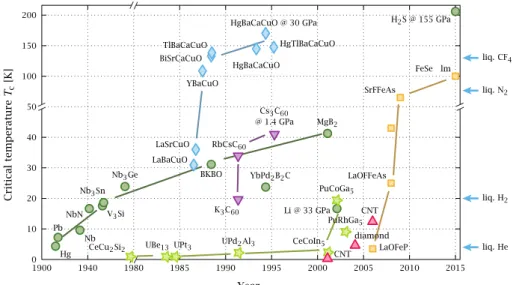
Nowadays superconductivity represents a broader phenomenon as seen in section2.1 and can be found on many metallic10elements of the periodic table, as, on many alloys, binary and ternary compounds, organic superconductors and lately discoveredHTS. A timeline with some of the more relevant superconductors found after the discovery of superconductivity phenomenon is represented in Figure 2.2 along with its maximum transition temperatures, Tc, and reference cryogenic materials used to cool them.
Research on different types of superconductors continues with prolific achievements, improving the already known and synthesizing new ones. In this thesis, the focus is pointed to those with the increased Tc known as HTS, due to economic viability and reduced cooling costs with liquid nitrogen, for power applications.
8BSCCOhere with a generic composition of (Bi, Pb)
2Sr2Can−1CunO2n+4is presented in two varieties (n = 2 or 3).
9Note that, 1 GPa (giga-Pascal) = 10000 bar or 10 kbar.
10Note that, the most conductive ones like gold, silver and copper are excluded since their lattice does not provide the necessary conditions for the occurrence of superconductivity (Eck,2018; Pina,2010)
2 . 2 . H I G H -T E M P E R AT U R E S U P E R C O N D U C T I N G M AT E R I A L S
Figure 2.2: Timeline of some known superconductors. Special note for the cuprates (blue dia-monds) where theBSCCOandYBCOare inserted). Taken from Jensen Ray (2015).
2.2.1 Available Commercial Forms
HTSmaterials commercially available in the market and considered for technological applications are predominantlyYBCOandBSCCOvariants, under bulk, wire and tapes.
• Bulk Materials
Bulks made out ofYBCOare the main available form with two different structures. Monocrystalline with higher current densities or the polycrystalline with strong anisotropy, in which, the current is limited by high-angle grain boundaries that increase barriers to the current flow, acting as weak links (Krabbes et al., 2006; Pina,2010; Seidel, 2015). Figure2.3shows a bulk material withYBCOcomposition available in the market.
Figure 2.3: Seeded melt growth bulk fromYBCOsupplied as levitation disks with Tc∼90 K and
trap magnetic field up to 1.4 T. Taken from Can Superconductors s.r.o. (2018).
Materials in this form are obtained byMelt-Textured Growth (MTG)processes, es-pecially by modified techniques asTop-Seeding Melt Texture Growth (TSMTG), which permit the manufacture of single or multiple grain superconductors (Krabbes et al.,2006;
C H A P T E R 2 . L I T E R AT U R E R E V I E W
Lehndorff,2001). In this technique, analloy of rare-earth elements with Barium-Copper-Oxide, RE123 (REBCO)crystals as Sm123 or Nd123, with a higher melting temperature than Y123 are put on top of the precursorYBCOcompacted pellet, serving as nucleation centres where crystallization starts and subjected to annealing treatment cycles to build the bulk.
• Superconducting Wires
HTS wires are essentially made of BSCCO material, and the Bismuth-Strontium-Calcium-Copper-Oxide, Bi2Sr2CaCu2O8+x(Bi-2212)variant is used to build round-wires and multifilamentary strands, using the knowledge gained onLTSwires and cables (De Marzi et al.,2016; Senatore et al.,2014).
Bi-2212is very brittle, therefore, is subjected toPowder-in-Tube (PIT)techniques as shown in schematic of Figure2.4, and to heat treatment processes with the diffusion of oxygen intoHTScomposites to form the conductors which are then filled into sheaths of silver alloys used to stabilize them.
Figure 2.4: A schematic outline of thePITprocess used to manufactureLTSwires and cables, as well forHTSmultifilamentary wires, strands and tapes. Taken from Lehndorff (2001).
This fabrication process uses also sufficient cold work and multifilamentary extrusion as seen in Figure2.4, and a cross-section ofBi-2212multifilamentary round wire manu-factured by Oxford Superconducting Technologies (OST) company is shown in Figure2.5 where superconducting filaments and silver sheath are observed.
2 . 2 . H I G H -T E M P E R AT U R E S U P E R C O N D U C T I N G M AT E R I A L S
Figure 2.5: Cross-section of a Bi-2212 multifilamentary round wire manufactured by OST com-pany. Taken from De Marzi et al. (2016).
• Tapes
Two kinds of tapes are currently available in the market and are differentiated byHTS used and the fabrication process involved (De Marzi et al., 2016; MA, 2004; Senatore et al.,2014):
i. The first kind is known as thefirst generation (1G) HTStapes and usesBSCCO ma-terials, theBismuth-Strontium-Calcium-Copper-Oxide, (Bi, Pb)2Sr2Ca2Cu3O10−x (Bi-2223)variant, essentially.
Bi-2223tapes use pure powders ofBi-2212phase and other precursor oxides, packed usingPITtechniques combined with overpressure methods and silver alloys sheaths as a stabilizer. This allows better flexibility and mechanical robustness character-istics, e.g., more feasible for coils and power transport cables. However, this kind of tapes tends to be more sensitive to magnetic fields, especially the perpendicular components which leads to great current density degradation (Pina,2010). Figure 2.6shows the cross-section of a1Gtape obtained by this methodology;
Figure 2.6: An optical micrograph with the cross-section of a1Gtape usingBi-2212materials manufactured by Beate Lehndorff at CryoElectra GmbH, showing a matrix of 15 superconducting filaments inside a silver sheath. Taken from Lehndorff (2001).
ii. The second kind is known as the2G HTStapes, or simplyCoated Conductors (CC), and uses YBCO materials. In this kind of conductors, PIT techniques cannot be used11due to a more pronounced crystal grain misalignment inYBCOmaterials, 11According to De Marzi et al. (2016) and Lehndorff (2001), one of the reasons thatPITtechnique cannot be used to manufactureCC, is due to platelet structure of micro crystals inside the microstructure during its deformation because they do not glide over each others so easily, thus not favouring the texture formation.
C H A P T E R 2 . L I T E R AT U R E R E V I E W
nor is e.g., possible to obtain round cables from it. Instead, techniques as thin epitaxial films deposited onto flat and flexible metallic tapes coated with buffering metal oxides and stabilizing layers are used to prepare high-performance supercon-ducting conductors. An illustration of a layered architectureCCcommercialized by SuperPower company is shown in Figure2.7, aims to demonstrate this methodology.
Figure 2.7: Generic schematic of a layered architecture for a Coated Conductor manufactured by SuperPower Inc. company. Taken from SuperPower-Inc. (2014).
CC due to its improved properties, such as the mechanical robustness, operation at a higher magnetic field and critical current is considered more relevant for the planned work of present thesis.
2.2.2 Applications of HTS Materials
Superconducting materials, in general, can be used in many practical applications and its use has been growing over the years.
LTSmaterials have been dominant in the market with steady growth, mostly in health applications using high field magnets forMagnetic Resonance Imaging (MRI)and Nu-clear Medical Resonance (NMR). Research in high energy physics for complex systems like the Large Hadron Collider (LHC)atCERNor the Facility for Antiproton and Ion Research (FAIR)in Darmstadt, Germany, are other areas of strong applicability, as are the nuclear fusion in projects like theInternational Thermonuclear Experimental Reactor (ITER),Wendelstein 7-xand others.
HTSmaterials due to their advantages have a growing share in the market. Applica-tions like passive high-frequency and microwave devices constituted byYBCOthin films in the electronics field, or the materials characterization, scientific instrumentation and geophysical exploration usingSuperconducting Quantum Interference Devices (SQUIDs) magnetometers due to its ultra-high magnetic field sensitivity, are just a glimpse of the broader spectrum of possible applications (Luiz et al.,2011; Pina,2010; Seidel,2015).
2 . 3 . C OAT E D C O N D U C T O R S
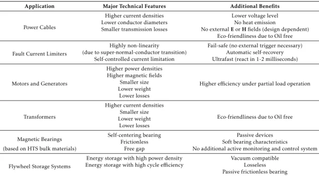
Processing machines and the transportation area whereMagnetic Levitation (MagLev) projects are taking major advances are other applications in the industrial field, in addi-tion to, new medical applicaaddi-tions or the main purpose here, in the power energy field. Table2.2aims to give an overview of some applications whereHTSmaterials are currently emerging.
Table 2.2: Emerging Industrial and Energy applications forHTSmaterials, according to CONsortium of European Companies determined To Use Superconductivity.
Adapted from Conectus.org (2018).
Application Major Technical Features Additional Benefits
Power Cables
Higher current densities Lower voltage level Lower conductor diameters No heat emission
Smaller transmission losses No external E or H fields (design dependent) Eco-friendliness due to Oil free Fault Current Limiters
Highly non-linearity Fail-safe (no external trigger necessary) (due to super-normal-conductor transition) Automatic self-recovery
Self-controlled current limitation Ultrafast (react in 1-2 milliseconds)
Motors and Generators
Higher power densities
Higher efficiency under partial load operation Higher magnetic fields
Smaller size Lower weight
Lower losses
Transformers
Higher current densities
Eco-friendliness due to Oil free Smaller size
Lower weight Lower losses
Magnetic Bearings Self-centering bearingFrictionless Soft bearing characteristicsPassive devices
(based on HTS bulk materials) Free gap No additional active monitoring and control system Flywheel Storage Systems
Energy storage with high power density Vacuum compatible Energy storage with high cycle efficiency Losseless
Passive frictionless bearing
2.3
Coated Conductors
Superconductivity effect is strongly anisotropic owing to grain boundary orientation of polycrystalline material. Thus, for an increasing misorientation of angles between adjacent crystallites, the superconducting currents are easily interrupted at interfaces between the crystals of superconductor, which leads the critical current density falling off exponentially. However, in tape form, these materials still present high-performance superconducting properties (De Marzi et al.,2016; Lehndorff,2001; Saxena,2010).
2.3.1 Manufacturing Process
CCmanufacturing is accomplished by a thin film technology, which is justified by the fact that film texture can be reliably controlled through an epitaxial process, achieving the best Jcfor this type of tapes. In a brief, the manufacturing process consists mainly of two stages according to De Marzi et al. (2016) and Senatore et al. (2014,2016):
C H A P T E R 2 . L I T E R AT U R E R E V I E W
i. Preparation of textured template, which includes buffer layers to prevent metal elements diffusion into the superconductor during high-temperature processing (MA,2004). This is achieved by two approaches, throughRolled Assisted Bi-Axially Textured Substrates (RABiTS)orIon Beam Assisted Deposition (IBAD);
ii. Deposition of a superconducting activeREBCOlayer on the template. This process can be achieved by several techniques, and the most used in the manufacturing industry are either by chemical processes asMetal-Organic Deposition (MOD)and Metal-Organic Chemical Vapour Deposition (MOCVD)or by physical techniques asReactive Co-Evaporation (RCE)andPulsed Laser Deposition (PLD).
These two stages are completed with the addition of silver and copper thick layers, which completes the conductor providing environmental protection and thermal stabi-lization, respectively. Figure2.8illustrates briefly these two main approaches used by the superconductors manufacturing industry.
Figure 2.8: A summarizing schematic of manufacturing methods for 2G CC, IBAD (left) and RABiTS (right), respectively. Taken from Celentano and Augieri (2012)
• RABiTSprocess
Rolled Assisted Bi-Axially Textured Substrates approach consists of the deforma-tion of a NiW metal alloy substrate (with reduced magnetizadeforma-tion and higher mechanical strength) through processes of rolling and recrystallization annealing. Followed by de-position of epitaxial buffer layers of Y2O3, CeO2andYttrium-Stabilized Zirconia (YSZ)
onto the textured NiW substrate, serving to block the inter-diffusion of substrate atoms and to provide lattice match for the growth of superconducting layer.
Currently, instead of NiW metal alloys, developments are being oriented towards sub-strates characterized by reduced ferromagnetic behaviour to minimize losses by hysteresis especially for power applications (Senatore et al.,2014).
2 . 3 . C OAT E D C O N D U C T O R S
• IBADprocess
Ion Beam Assisted Deposition use stainless steel or polycrystalline Hastelloy tapes submitted to an electropolishing process. A diffusion-barrier layer of Al2O3and a seed layer of Y2O3are deposited onto the surface of the metallic substrate by a sputtering
tech-nique, followed by the deposition of a biaxially textured layer of MgO with an assisting 1 keV Ar+ion beam in a standardPLDgeometry.
IBADprocess reduces the surface roughness from ~50 nm to less than 2 nm, generat-ing a preferred texture in the buffer layers. Is the most used by current manufacturers. Table2.3gives an overview of these superconductors manufacturers and the main pro-cesses applied.
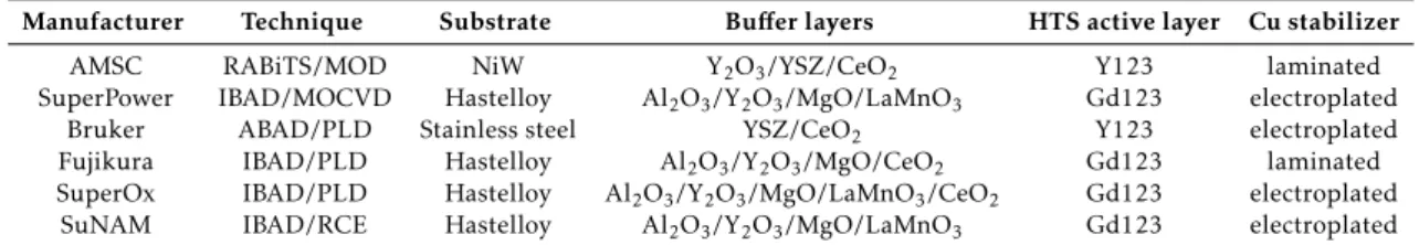
Table 2.3: Fabrication key parameters forCCamong the industrial superconductors manufacturers. Adapted from Senatore et al. (2014,2016)
Manufacturer Technique Substrate Buffer layers HTS active layer Cu stabilizer
AMSC RABiTS/MOD NiW Y2O3/YSZ/CeO2 Y123 laminated
SuperPower IBAD/MOCVD Hastelloy Al2O3/Y2O3/MgO/LaMnO3 Gd123 electroplated
Bruker ABAD/PLD Stainless steel YSZ/CeO2 Y123 electroplated
Fujikura IBAD/PLD Hastelloy Al2O3/Y2O3/MgO/CeO2 Gd123 laminated SuperOx IBAD/PLD Hastelloy Al2O3/Y2O3/MgO/LaMnO3/CeO2 Gd123 electroplated
SuNAM IBAD/RCE Hastelloy Al2O3/Y2O3/MgO/LaMnO3 Gd123 electroplated
For a larger commercial diffusion ofCC, manufacturers are focusing on some impor-tant aspects which can not be dissociated, namely:
i. Performance of produced tapes, which shows large variability when comparing from different manufacturers at temperatures of 77 K in self-field and at 4.2 K in high-field (i.e., 19 T), without univocal correlation between critical current values (Senatore et al.,2016);
ii. Length of manufactured tapes, owing to the demand of different sectors. At the electric utility sector there are no rigorous requirements concerning a single-piece length, the coil manufacturers, on the contrary, demands longer pieces of tapes with enhanced mechanical properties.
Bruker company, e.g., produces 12 mm wide tapes up to 300 m length with Ic of
420 A (at 77 K, self-field). However, there is a consensus for the energy sector that more than 1000 m are necessary for applications likeSFCL, transformers, industrial motors or generators according to Celentano and Augieri (2012) and MA (2004). Besides, hundreds of kilometres of tape are necessary to build a 1 km long power cable according to Senatore et al. (2014);
iii. Tape’s price is another key factor considering thatCCcosts are essentially due to large investments in research and production infrastructures. In addition, power
C H A P T E R 2 . L I T E R AT U R E R E V I E W
devices manufacturers demand prices four times less than practised. Thus, there is a clear conviction that an improvement on current methods and a more efficient production will result in a reduction of tape’s final price.
2.3.2 Coated Conductors Constraints
CCin the market are characterized by a diverse constitution and obtained with dif-ferent combined techniques as seen in Table2.3. In particular, an interiorREBCOlayer of intrinsic brittleness is used, presenting different mechanical and electromechanical properties. Therefore, it is important to address some situations which can lead to par-tial or complete damage considering the involved strain when in operation. Figure2.9 illustrates different types of strain which aCCtape can be subjected.
Figure 2.9: Illustration of different strain types and mechanical strength on a Coated Conductor. The stress values correspond to a tape with electroplated copper stabilizer. Taken from Maeda and Yanagisawa (2014).
Manufacturers already offer tapes with good mechanical strength, but as illustrated in Figure2.9,CCpresent an anisotropic mechanical strength. As a result, important care must be taken in order to avoid damages at the superconducting layer when handling the tapes.
Supported on what is summarized in Figure2.9and according to Barth (2013), Maeda and Yanagisawa (2014), and Senatore et al. (2014), the following aspects should be con-sidered when usingCC:
i. In the transverse direction, tensile strength assume low values between 10-100 MPa, and it can introduce a problem owing to the forces acting to the normal direction of the tape surface;
ii. Cleavage strength (due to external forces acting to open one edge of the adhesive assembly) and peel strength (similar to cleavage with the exception that only one part of the adhered tends to be flexible) are extremely weak;
2 . 4 . C O I L S F R O M C OAT E D C O N D U C T O R S
iii. Critical axial tensile stress, depending on the copper fractional area in commer-cial available electroplatedCCcan be higher up to 700 MPa, superior to 430 MPa presently supported inBSCCOtapes with new lamination techniques;
iv. Tapes laminated with materials of large thermal contraction allows the highest strain limits (Senatore et al.,2014);
v. Delamination12 at the interface between layers ofCC can occur when applied a sufficient strain, and these consequences are mentioned in literature by several au-thors, e.g., in Barth (2013) and Senatore et al. (2014).
Devices likeWalters Spring (WASP)are used to measure the strain dependence of critical current of superconductors with relatively long length. For this purpose, the superconductor is wound along the outer surface of a spring in which a torque is applied, resulting in an axial strain over the superconductor (Barth et al.,2015; Sugano et al.,2008);
vi. The electromagnetic strain13 may degrade irreversibly the critical current of CC during operation. Observe that, conductors hoop stress14 can limit the overall current density onHTS applications, if not limited in 500-700 MPa range, e.g., a REBCO NMRcoil is subjected to enormous longitudinal stresses, ≈ 500 MPa (Barth et al.,2015; Barth,2013; Maeda and Yanagisawa,2014);
Summarizing, along with the magnetic field and the operating temperature, the me-chanical strain also influences the superconductor’s current carrying capabilities.
2.4
Coils from Coated Conductors
Coils represent an important part for the construction of differentHTSdevices, and several topologies have been advanced. This section describes the necessary steps found in the literature to build coils, including the cut of tapes and the necessary joints to splice and finish.
Magnets have been along the years a great booster in the development of coils using HTSmaterials, where aspects like the winding process, coil impregnation and insulation, pose great challenges, as do the cut and joint process.
12Delamination has not been reported as a problem forBi-2223tapes, despite the lower strength values showed in tests when comparing againstCC, according to Senatore et al. (2014).
13Note that, Lorentz forces affect the conductor longitudinally in tension.
14Hoop stress is the axial tensile along the longitudinal direction of the conductor in solenoidal magnets. Therefore, the conductor substrate metal should be strong enough to bear most of this stress in order to limit the strain on the superconducting layer.
C H A P T E R 2 . L I T E R AT U R E R E V I E W
2.4.1 Winding Processes
Two main techniques have been used to windHTShigh-field magnets along the years, namely,Layer-Wound (LW)andPancake or Double-Pancake (DP):
i. LWtechnique, use a single conductor piece which is wound from the innermost to outermost layers, turn by turn one layer at a time;
ii. DPwith the height of twice the tape width, two pancakes are wound sequentially from a midpoint of the conductor, spiralling radially outward from the innermost to outermost turns, and thecross-over from one pancake to other occurring at the
innermost turns without interruption (Senatore et al.,2014).
Certain constraints must be taken into account as seen in section2.3.2when usingCC. The winding process can introduce bending strains which can occur along the conductor axis and known aseasy bending or normal to the conductor axis known as difficult bending, e.g., at the inner transition region in aDPcoil or each end of anLWcoil. Therefore, for large winding diameters there is no big issue, on the contrary, for diameters less than 50 mm, some design constraints are imposed.
In addition to usual winding techniques, new configurations have been studied and tested. Figure2.10shows in(a)a short-circuitedDPcoil made withCCby aNo-Insulation (NI)winding technique. It was developed by Qu et al. (2016) to test aPersistent Current Mode (PCM)switch to be used in high-fieldHTSmagnets, e.g.,NMRandMRI, instead of driven mode operation in which these applications operate when usingREBCOmagnets. In(b)a schematic panoramic view illustrates the resistive pancake-pancake (P-P) joint between top and bottom pancakes terminals.
(a)
(b)
Figure 2.10:(a)short-circuitedDPcoil wound byNIwinding technique mounted to test the (P-P) resistive joint;(b)schematic panoramic view illustration of the coil. Taken from Qu et al. (2016).
2 . 4 . C O I L S F R O M C OAT E D C O N D U C T O R S
A low-resistanceHTSshort-circuited coil using theLWtechnique is shown in Figure 2.11. It was developed by Murta-Pina et al. (2018) using a new engineering design that allows a single joint independent from the number of turns and is intended for medium voltage applications such asSFCLwhere a short-circuitedHTSsecondary is used.
Figure 2.11: A low-resistanceHTSshort-circuited coil using theLWtechnique and made withCC. Taken from Murta-Pina et al. (2018).
Figure2.12shows in(a)a ring-shape2G HTSmagnet inspired in thewind-and-flip15
method proposed by Sheng et al. (2017). This approach uses a stack of ring-shapedCC to build trapped-field magnets and is intended to provide feasible sizes according to the pieces of tape used and the slits made on it to achieve the desired diameter.
(a) (b)
Figure 2.12: Jointless continuousHTScoils:(a)a ring-shape2G HTSmagnet, adapted from Sheng et al. (2017);(b)aDPcoil using a singleCCsplit into two tapes and wound by thewind-and-flip
method, adapted from Kim et al. (2015).
In(b)aDPcoil without any electric joints proposed by Kim et al. (2015) is shown. It uses a single wide CCsplit longitudinally in the middle as shown by the schematics illustrated in (a). This coil is wound by the wind-and-flip method and was proposed
to be used in PCMoperation on magnets, i.e.,NMRandMRIapplications, as inSFCL, nevertheless, are not scalable for medium voltage devices (Murta-Pina et al.,2018).
15Wind-and-flip is a method intended to avoid non-superconducting joints and consists of a closed loop for the current created by longitudinal partial slices in CC. For this purpose, each slice is wound in a coil shape and one of the coils is flipped to avoid field cancelling. Detailed information on this method can be found in Seyeon Lee et al. (2013) and Woo-Seok Kim et al. (2009).
C H A P T E R 2 . L I T E R AT U R E R E V I E W
• Coil Impregnation and Insulation
Coils can be constructed with or without impregnation. Impregnation permits to fill a void-filled winding into a solid monolithic structure, with the advantage of mechanically stabilize the conductors distributing equally the loads along the axial direction. There-fore, helping to immobilize against electromagnetic forces.
Impregnation is done by using glues, epoxy resins, waxes, paraffin and solders. In brief, materials16with extremely low thermal contraction, allowing the reduction of ther-mal stress on the edge of superconductors due to the mismatch of the therther-mal contraction coefficients among the impregnation materials and CC (Barth,2013; Goldacker et al., 2014; Senatore et al.,2014).
For the insulation, which prevents the current from passing between the conductor’s turns,CCmanufacturers suggestKapton tape, but the use of enamel (used for insulation
of NbTi wires) is also recommended on the literature. According to Badcock et al. (2009) and Senatore et al. (2014), the UV curable varnish is also used to insulate slitted strands of Roeble cables, and also thermally-cured and UV-cured polymer coatings, oxide physical vapour deposition, oxide sol-gel coating, polyester heat-shrink tubing and the electro-deposited polyamide insulation are some of the other insulation techniques tested.
2.4.2 Cutting Methods
In order to avoid some of the issues described in section2.3.2, the most indicated methods must be considered to cut theCC, since the layers of superconducting material (ceramic and brittle) under the protection of substrate and stabilizer layers can be dam-aged. For this purpose, some of the methods found in the literature are described in this section as follow:
i. Laser cut with conventional machines uses heat to melt the material and has been used for many years to cut several types of materials with good flexibility, results and cutting rates, including ceramic, composites and laminated materials. However, owing to heating and melting defects imposed by the laser it does not show good results when used to cut coated conductors.
Another laser variant tested is the picoseconds-infrared laser technology, which permits to avoid defects on the tape, but it is not appointed as economically viable in terms of production speed (Goldacker et al.,2014);
16Observe that, materials used for impregnation and into coated conductors can expand if heated or contract if cooled, causing a certain deformation of its lattice and resulting in thermal stresses. Additionally, a mismatch of the thermal expansions of the materials during the cool down process can result in damages onREBCOtapes, which may lead also to the degradation of current carrying capability.
2 . 4 . C O I L S F R O M C OAT E D C O N D U C T O R S
ii. Electrical Discharge Machining (EDM)tested and reported by Senatore et al. (2016) to cut tapes with laminated stabilizers, reducing till 2 mm width of tape with a single cut from one side, can also be considered depending on the tapes’ structure. This technique creates sparks that melt tiny portions of the material without gen-erating cutting forces. It is a useful approach but requires electrically conductive materials;
iii. Water jet cut uses supersonic erosion to remove the material, using or not an abra-sive (usually for tougher materials) and is one of the most versatile and fastest cutting processes in use at Industry. This process presents as advantages, the cold cutting, i.e., no heat affected zone, low stress, no warp on the material and is con-sidered environmentally friendly. At present, there are no records on literature referring strictly the use of this cut method forCCwithout the addition of any other technique;
iv. A technique tested by Heilmann (2013) combines both water jet and laser cut. A fibre-coupled pulsed diode pumped solid state laser is combined with a water jet guided system, in order to minimize the burr height and the heat caused by the laser during the cut. This is an elaborated process where parameters as the laser power and repetition rate, the tape velocity through the machine and the water pressure need to be carefully chosen and optimized in order to obtain good cut results. Nonetheless, the authors report critical current losses of 16% in tapes cut by this method when compared with untreated tapes.
v. Mechanical punching technique is identified by theKarlsruhe Institute of Technol-ogy (KIT)and the Industrial Research Limited (IRL) as the more suitable method to cutCCaccording to Badcock et al. (2009) and Goldacker et al. (2014).
(a) (b)
Figure 2.13: Fabrication of Roeble cables by the mechanical punching technique. Adapted from Goldacker et al. (2014):(a)A reel-to-reel computer-controlled pneumatic punching machine at KITto produce Roebel strands;(b)Ten strands punched from a 12 mm wide CC (top), Assembled Roeble cables from the strands (bottom).
C H A P T E R 2 . L I T E R AT U R E R E V I E W
This technique uses a reel-to-reel computer-controlled pneumatic punching tool, shown in Figure2.13. As advantages, allows high-speed production of strands with good precision, i.e., typically 50 m of tape per hour with less than 50 µm of loss at each slit, flexibility and the possibility to adjust the tool for different cut geometries, producing strands with current carrying capability losses less than 2-3% for homo-geneous CC (Goldacker et al.,2014).
Several Roeble cables which are made by meander-shapedCCstrands and assem-bled as shown in Figure2.13to reduce induced eddy currents, current loops and consequently the ac losses on power cables, use this punching technique to obtain the desired strands.
vi. A less elaborated method, such as a regular stainless-steel electrician scissor was also tested by Murta-Pina et al. (2018) with good results for the final critical current measured on tapes cut by this method, showing no visible delamination. Neverthe-less, for large-scale cutting processes, it is not feasible.
2.4.3 Junction Methods
Joints pay a key role to obtain good superconducting devices, which require electrical connections between superconductors and other parts that constitute them. Several stud-ies found in the literature focus on the development of good techniques to bond theCC in order to achieve excellent joints.
• Types of joints
According to Brittles et al. (2015) and Kato-Yoshioka et al. (2006), these techniques can be classified as superconducting or non-superconducting joints:
i. Superconducting joints use direct bonding approaches such as the solid state dif-fusion under uniaxial pressure, melting and melting-difdif-fusion. These techniques involve high temperatures, followed by a prolonged oxygenation-annealing process to recover the degraded superconducting properties ofHTSlayers, which lose oxy-gen at high temperatures due to its crystalline nature (Barth,2013; Brittles et al., 2015; Senatore et al.,2014).
An excellent result for a superconducting joint was reported by Park et al. (2014), it is based on atomic diffusion with partial melting of internalREBCOlayers in the CCand was accomplished by a series of processes, namely:
a) Removal of stabilizer layers by a chemical etching to access theREBCOlayer; b) Micro-holes by laser on tape to facilitate oxygen diffusion;
c) Heat treatment for joining in vacuum at a peak temperature of 850℃; 22
2 . 4 . C O I L S F R O M C OAT E D C O N D U C T O R S
d) Oxygenation annealing under high-pressure oxygen at 500℃ to increase the oxygen content of theREBCOlayer and restore its superconducting properties.
As a result, it allowed the establishment of a resistance-free closed loop forPCM operation, steady for 240 days with total circuit resistance of <10−17Ω(i.e. perfect electrical connection).
ii. Non-superconducting joints (also known as resistive joints), on the contrary, allow more flexible geometries and use a low melting point metal as a soldering material, filled between the contact area of the tapes.
This approach is expected to result in a higher joint resistance value, owing to the sum of resistances of soldering material and tape stabilizing layers. Thus, the joint resistance using this technique varies over orders of magnitude, depending on tape and solder types used in the joining process. According to Senatore et al. (2014) values of specific resistivity, i.e., resistance times joint area, between 30-500 nΩcm2 and measured at 77 K, are reported as good ones.
The main types of configurations used to build joints using the techniques presented above are illustrated in Figure2.14, where a schematic of a non-superconducting joint is indicated for both lap and bridge configurations.
Figure 2.14: Original schematic of the main types of joint configurations in use (lateral view): (top) lap joint and (bottom) bridge joint. Taken from SuperPower-Inc. (2014).
A study developed by Duckworth et al. (2010) with the objective to verify a repro-ducible method to obtain low-resistance and high-mechanical-strength joints, appoints that joints of lowest resistance (e.g., between 20-100 nΩ in 4 mm width tapes) are influ-enced by the tapes’ orientation in the joint and its stabilizers material, i.e., best results with electroplated copper stabilizer, see Table2.3for reference.
Another factor usually considered, is the solder applied on tapes through the super-conductor side, rather than the substrate side, i.e., in a face-to-face configuration. With the lap configuration producing the best results according to AMSC (2012).
C H A P T E R 2 . L I T E R AT U R E R E V I E W
Optimization ofCC is a constant goal for manufacturers, who align the supercon-ductor layer in a longitudinal way on tapes in order to make the current flow easily. Considering this factor, a conceptual sketch of bridge joint variants is illustrated in Fig-ure2.15from a study developed by Chang et al. (2011) on the effect of the direction of the joints inHTSapplications such asNMR, where it is important to ensure the homogeneity of the magnetic field.
Figure 2.15: Sketch of bridge joint variants: (left) parallel direction (PD joint) with the CC and (right) orthogonal direction (OD joint) relative to theCC. Adapted from Chang et al. (2011).
In this study, the auxiliary pieces of the tape were overlapped in a parallel or orthog-onal direction toCC, achieving joint resistances between 40-140 nΩ. Therefore, three important remarks from this study:
a) Considering the same overlap tape width, bridge joints in parallel direction offer better results rather than in orthogonal;
b) The narrower the overlapping tape, the lower the joint resistance;
c) Lap joints produce better results than bridge joints, in terms of joint resistance and critical current.
• Temperature and applied Pressure
During the joining process, temperature and the applied pressure on the contact area are important aspects to consider also, in order to obtain a low joint resistance preserving the superconducting properties of the tapes in contact.
As exposed in section2.3.2, it is important not to exceed the transverse stress limits of theCC, and there are guidelines from AMSC (2012) and SuperPower-Inc. (2013) on how to perform low-resistance splice joints with recommendations for temperature thresholds on these procedures.
A study developed by Bagrets et al. (2015) on the dependence of joint resistance with the applied pressure for non-superconducting joints, appointing two types of contacts:
a) Soldered joints, between tapes (with applied pressures till 10 MPa);
b) Mechanical pressed (also mechanical joints), with applied pressure till 25 MPa. Useful for stacked tapes insideHTScables.
2 . 4 . C O I L S F R O M C OAT E D C O N D U C T O R S
Some examples of devices found in the literature and used to make joints between tapes are shown in Figure2.16.
(a) (b) (c)
Figure 2.16: Different kinds of soldering devices used to make joints: (a)Schematic of a holder device, adapted from Kato-Yoshioka et al. (2006);(b)A soldering device, adapted from Bagrets et al. (2015);(c)A soldering machine with real-time temperature control, adapted from Ki Sung Chang et al. (2010).
In(a)a holder device made of Inconel used by Kato-Yoshioka et al. (2006) for joining by diffusion. Joint resistances between 0.02-0.03 µΩ for a joint area of 40 mm2 were
achieved with an applied pressure (controlled by torque on the screws) between 10-60 MPa at room temperature. They also registered a decrease of the critical current for an applied pressure above 30 MPa.
In(b)a soldering device with resistive heating on base, pressuring punch and spring to control the applied pressure used by Bagrets et al. (2015), which appoint the range 5-10 MPa as reasonable values to achieve a low-resistance contact.
In(c)a soldering machine developed by Ki Sung Chang et al. (2010), to make joints on various bending diameters (100-150 mm), is comprised of a temperature control part with thermal sensors and cartridge heaters which control, monitor and adjust the temperature in real-time, and a soldering part where the heat and pressure are applied.
• Soldering Materials
For the realization of non-superconducting joints, the soldering materials can be acquired in different forms, e.g., powders in-tube, ribbon solder or premixed. The choice of which one to use is according to practical application, and the preference should take into consideration the following aspects:
a) A low melting point, in order to bond the tapes with a lower possible temperature; b) Lower electrical resistivity, to get the best electrical connection between the
C H A P T E R 2 . L I T E R AT U R E R E V I E W
c) Higher thermal conductivity, to ease the heat transfer between theCCand rest of the components in the systems where it is inserted;
d) Similar thermal expansion coefficients, since a large mismatch of the coefficients between theCCand soldering materials, can cause stresses, thus damage theCC.
The use of premixed solder pastes or ribbon solders helps to accomplish more homo-geneous resistive joints. According to Senatore et al. (2014), the best results are achieved with two-component alloys (e.g., SnAg, InSn, SnPb), with tin and lead prices per gram as the cheapest in the market (Tsui et al., 2016). Table2.4 lists some lead-free solders compositions usually recommended by manufacturers for low-resistance joints.
Table 2.4: Recommended solders compositions by manufacturers, Pb-free. Information adapted from (Indium-Corporation,2016).
Composition Melting Temperature Electrical Conductivity Thermal Conductivity Thermal Coefficient of Tensile Strength
(%) (°C) (% of IACS) (W/cm°C @ 85 °C) Expansion (PPM/°C @ 20 °C) (MPa)
100In 157 24.00 0.86 29 1.88
52In 48Sn 118 11.70 0.34 20 11.86
96.5Sn 3.5Ag 221 16.00 0.33 30 39.99
96.5Sn 3.0Ag 0.5Cu 220-217 - - - 49.64
2.4.4 Applications of HTS Coils
TheHTSmaterials as exposed in Table2.2have many applications in the industrial and energy sector, andHTScoils, in particular, can be used in power applications such as theSFCL, detailed as follows due to its specific interest for the present thesis.
SFCL are devices with intrinsic non-linear resistivity owing to the HTS materials which constitute it, acting as a natural fault current limiters. Such devices present a negligible impedance in normal conditions where it can carry high current densities (i.e., in superconducting state), whereas in cases of currents above a certain threshold (e.g., under a fault) its state switch to a higher impedance due to the loss of superconducting properties (i.e., normal state). Nevertheless, It returns to normal conditions once the fault is suppressed (Pina et al.,2010).
These devices in nominal conditions, when included in anElectric Power Grids (EPG) contribute to transient stability of the generators, thus for global stability of the grid owing to the good transition from the superconducting to resistive or inductive states in fault situations. This behaviour allows a reduction of short-circuit currents in the order of 20-50% within milliseconds, whereas 30% is already considered an adequate safety mar-gin for the network types of equipment (Didier and Lévêque,2014; Didier et al.,2015).
Amongst the differentSFCL, the emphasis goes to resistive and inductive topologies, mature technologies with several practical applications mentioned in the literature.