Brazilian Journal of Physics, vol. 36, no. 2A, June, 2006 405
InGaAs Embedding of Large InAs Quantum Dots Obtained by Pulsed In
Deposition for Long-Wavelength Applications
T. E. Lamas and A. A. Quivy
Laborat´orio de Novos Materiais Semicondutores, Instituto de F´ısica, Universidade de S˜ao Paulo, CP 66318, 05315-970 S˜ao Paulo, SP, Brazil
Received on 4 April, 2005
In this work we studied the molecular-beam epitaxy of large InAs quantum dots embedded in an InGaAs quantum well. The formation of the quantum dots was performed by pulsed deposition of InAs material, simu-lating therefore a low deposition rate. Room-temperature photoluminescence experiments carried out on these samples showed intense emissions with a wavelength exceeding 1.35µm. Our preliminary data indicate that even better results can be achieved by further manipulation of the growth conditions.
Keywords: Molecular-beam epitaxy; InAs quantum dots; InGaAs quantum well
I. INTRODUCTION
In recent years, there has been a great interest in the growth of InAs self-assembled quantum dots (QDs) with optical ac-tivity around 1.3 and 1.5µm, which are the most important windows for optical-fiber communication networks. There are two main approaches to tune their emission around these wavelengths: by employing low InAs growth rates (lower than 0.01ML/s instead of the conventional value of≈0.1ML/s) or by embedding the InAs QDs in InGaAs layers (forming the dots-in-a-well (DWELL) structure). It has been proved that the first technique provides larger QDs [1], leading thus to an increase of the emission wavelength when compared to con-ventional (smaller) QDs. The second approach takes advan-tage of the reduction of both the confinement potential for car-riers in the QDs (InGaAs barcar-riers instead of GaAs) and the strain in the InAs QDs, yielding a redshift of the emission [2]. Several reports already showed QDs emission reaching [3] (and even going beyond [4, 5]) 1.3µm by using separately one of these methods, but there are only a couple of works aimed to explore the combination of both techniques [6] to get longer wavelengths or eventually better optical properties. The main problem is that most molecular-beam epitaxy (MBE) systems have only one single In cell. When the In cell is set up to a low InAs deposition rate for QDs growth (≈0.01ML/s), the deposition rate of the InGaAs cap layer has also to be very low (≈0.06ML/s) in order to grow an alloy with an In con-centration in the range of 10-20%. In these conditions, the benefit of the redshift of the emission achieved with the large InAs QDs formed with a low growth rate is partially lost due to the enhancement of In segregation by the low growth rate of the InGaAs cap layer. One alternative would be to interrupt the growth after the QDs for a new setting and stabilization of the In deposition rate of the InGaAs cap layer, but several papers have already evidenced a blueshift of the emission for growth interruptions longer than 5 minutes [6, 7]. One way to avoid the drawback of a low growth rate during capping or a long growth interruption after the QDs formation is to em-ploy the nucleation-augmented method proposed recently by Chia and coworkers [8] to form large QDs. In this method, the QDs are initially nucleated using a conventional growth
rate and depositing 1.8ML of InAs, and the rest of the mate-rial is supplied by short pulses of In atoms. The interrupted arrival of In atoms on the surface has the same effect as a low deposition rate, allowing the evolution of the initial small QDs into larger QDs. In this work we report on the use of the nucleation-augmented method to grow large InAs QDs in a DWELL structure with a single In cell.
II. EXPERIMENTAL
Our samples were grown in a Gen II MBE system. The growth rates of InAs, GaAs and InGaAs were 0.1, 0.56 and 0.66 ML/s, respectively, yielding an In concentration of 15% in the InGaAs layers. After a 200nm GaAs buffer layer grown on a GaAs(100) semi-insulating substrate at 580oC, the sample temperature was lowered to 490oC and 2nm of In0.15Ga0.85As were grown. The InAs QDs were obtained by continuously depositing 1.8ML of InAs (nucleation layer) fol-lowed by 6 cycles of 1s of In and As supply alternated with 9s of As supply only (In shutter closed), leading to a total InAs thickness of 2.4ML. The effective growth rate Re f f of the InAs material during the pulsed deposition is given by:
Re f f=R×(tOtO+
tC)
continu-406 T. E. Lamas and A. A. Quivy
ously depositing 2.4ML of InAs in the same In0.15Ga0.85As quantum well used in sample A. In order to check the influ-ence of the number and period of the In-shutter cycles on the optical properties of our structures, a second set of samples was grown. Their structure was identical to the one of sample A but we employed different times tO and tC for the evolu-tion of the QDs after the deposievolu-tion of the 1.8ML-thick InAs nucleation layer. In the first sample (D), we employed 3 cy-cles with tO=2s and tC=18s. In the second one (sample E), we used 12 cycles with tO=0.5s and tC=4.5s,i.e., a larger num-ber of cycles with a smaller period. It is worth noting that, in both samples, the amount of InAs material deposited and the effective InAs growth rate were the same as in sample A. The optical emission of all the samples was investigated by pho-toluminescence (PL) using conventional lock-in techniques, the 514.5-nm line of an Ar+ laser and a germanium detector cooled with liquid nitrogen.
III. RESULTS AND DISCUSSION
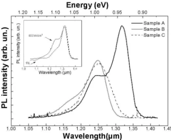
The room-temperature PL spectra of the first set of samples can be seen in Fig. 1. Sample C (DWELL with conventional QDs) shows a signal peaked at 1.24µm with a full-width at half maximum (FWHM) of 56meV. As a matter of fact, longer wavelengths can be achieved by using conventional DWELL structures but, in our case, this sample will only be a refer-ence and, therefore, further optimization is out of the scope of this work. For sample B, where the nucleation-augmented method was employed in a GaAs matrix, we can see a broad PL spectrum with two emissions centered around 1.25µm and 1.18µm. PL measurement as a function of excitation power allowed us to assign these peaks to the optical transition from the ground and first excited states of the QDs. The FWHM of the ground state obtained by curve fitting was 33meV. The most remarkable result of this set was found in sample A (DWELL with nucleation-augmented method), which also ex-hibited two emissions with the ground state peaked at 1.31µm with a FWHM of only 23meV. The inset of Fig. 1 shows the state-filling effect in the PL spectra taken at different excita-tion powers, confirming that the peak with longer wavelength is related to the ground-state transition. From these results, we can conclude that the nucleation-augmented method was able to shift the emission of a DWELL structure towards longer wavelengths. After the initial formation of the QDs with the continuous deposition of 1.8ML of InAs, the use of a pulsed In deposition yields a larger surface diffusion that allows most of the adatoms to incorporate into already existing QDs instead of nucleating new ones, increasing further their size and lead-ing to the observed redshift.
The objective of the second set of samples was to check whether a different timing of the shutter sequence could yield better results. Fig. 2 shows the PL spectra of these samples that will be compared with the one of sample A. In sample D, the QDs were formed by repeating 3 times a basic cycle con-sisting of 2s of InAs supply followed by a 18s-long exposure to As only. The PL spectrum of this sample shows a broad peak resulting from two emissions centered around 1.25 and
FIG. 1: Room-temperature PL spectra of sample A (DWELL with nucleation-augmented QDs), sample B (nucleation-augmented QDs in a GaAs matrix) and sample C (DWELL with conventional QDs). The power density was 800W/cm2. The inset shows two spectra taken on sample A with different excitation powers.
1.32µm. PL experiments performed under different excitation powers showed no appreciable change in the relative inten-sity of these two peaks, indicating that they are most prob-ably related to two different families of QDs. The shape of the spectra changed radically when shorter periods were em-ployed (sample A and E). As already mentioned above, sam-ple A exhibited a peak centered at 1.31µm with a FWHM of 23meV related to the optical transition from the ground state. The spectrum of sample E, which was grown with the shorter cycle of this set, showed a ground state emission centered at 1.35µm with a FWHM of only 24meV.
Brazilian Journal of Physics, vol. 36, no. 2A, June, 2006 407
FIG. 2: Room-temperature PL spectra of DWELL samples grown with the nucleation-augmented method using different cycles. The number of cycles, the period of time during which the In shutter was kept open and the period of time during which only the As shutter was kept open in each sample were, respectively: 3 cycles, 2s and 18s for sample D, 6 cycles, 1s and 9s for sample A and 12 cycles, 0.5s and 4.5s for sample E. The power density was 800W/cm2.
IV. CONCLUSION
In this work we employed the nucleation-augmented method to grow large InAs QDs in an InGaAs quantum well (DWELL structure). Intense and narrow PL signals were ob-served at wavelengths exceeding 1.3µm. Such an approach al-lows a wider variation of the growth parameters (mainly the In composition of the InGaAs quantum well and the InAs growth rate) which can be optimized in future works in order to in-crease the QDs size, to reduce In segregation and eventually to get more intense emissions and longer wavelengths.
Acknowledgement
We would like to thank CNPq and FAPESP (grants 98/12779-0, 02/10185-3 and 03/09398-5) for financial sup-port.
[1] Y. Nakata, K. Mukai, M. Sugawara, K. Ohtsubo, H. Ishikawa, and N. Yokoyama, J. Crystal Growth208, 93 (2000).
[2] V. M. Ustinov et al., Appl. Phys. Lett.74, 2815 (1999). [3] H. Y. Liu, M. Hopkinson, C. N. Harrison, M. J. Steer, R. Frith,
I. R. Sellers, D. J. Mowbray, and M. S. Skolnick, J. Appl. Phys.
93, 2931 (2003).
[4] E. C. Le Ru, P. Howe, T. S. Jones, and R. Murray, Phys. Rev. B
67, 165303 (2003).
[5] M. J. da Silva, A. A. Quivy, S. Martini, T. E. Lamas, E. C. F. da
Silva, and J. R. Leite, Appl. Phys. Lett.82, 2646 (2003). [6] A. Convertino, L. Cerri, G. Leo, and S. Viticoli, J. Cryst. Growth
261, 458 (2004).
[7] S. Kiravittaya, Y. Nakamura, and O. G. Schmidt, Physica E13, 224 (2002).