Raman spectroscopy of graphene: probing phonons, electrons and electron-phonon
interactions
Leandro Malard Moreira
Orientador: Prof. Marcos Assun¸c˜ao Pimenta
Tese de doutorado apresentado `a UNIVERSI-DADE FEDERAL DE MINAS GERAIS.
i
Agradecimentos
`
A minha fam´ılia, pelo amor e apoio.
`
A Tati, pelo seu amor e por me aguentar falando de trabalho.
Ao Markin, pela excelente orienta¸c˜ao e por dar apoio `as minhas ´ıdeias que quase sempre d˜ao errado. Por me ensinar a ser cr´ıtico e ver que fˆenomenos f´ısicos complicados podem ser entendidos de uma maneira simples. Pela sua amizade, cervejadas e churrascadas no Tangar´a.
Ao Ado, pela sua contagiante vis˜ao da nanociencia. Por todas as discuss˜oes de f´ısica ou de bobagem mesmo. Por me lembrar que existem algumas m´usicas da d´ecada de 80 que prestam, pelo menos uma, Katia Fl´avia.
Ao Gusta e ao Cris, pela grande ajuda no meu doutorado com discuss˜oes e ajudas t´ecnicas no lab.
Aos ramanistas, e aos nearfieldistas pelos in´umeros galhos quebrados, amizade e muiiiitooos caf´es.
A todo corpo t´ecnico e aos funcion´arios do departamento de f´ısica, porque sem eles n˜ao existe ciˆencia. Em especial `a Idalina por toda sua dedica¸c˜ao.
A todos os professores do departamento, pela ´otima convivˆencia, empr´estimos de material (que n˜ao foram poucos) e discuss˜oes pelos corredores. Em especial, ao M´ario S´ergio, Chacham, Elmo e Sampaio por sanar minhas d´uvidas de estado s´olido.
Ao Daniel, Juliana, Thiago, Jorge, Elmo e Fl´avio pela colabora¸c˜ao cient´ıfica.
Ao Antˆonio Castro Neto, pelas discuss˜oes no grafeno e constantes visitas.
aspects of the carbon nanoscience.
`
A ro¸ca do custela, da Fˆe e da J´ulia, `a Fazenda da Barra e ao Emprale.
A todos os amigos!!!
Ao Kimmel.
Ao CNPq, `a CAPES, `a FAPEMIG e `a Nacional de Grafite, que tamb´em acreditam na pesquisa cient´ıfica de qualidade no Brasil.
2006
2009
Figure 0.1: First picture from top to bottom left to right: Vladmir, Leo Campos, Paulo Ara´ujo, Ado J´orio, Daniela Mafra, Leandro Malard (Xubaka), Mathias Steiner, Rodrigo Gribel, Daisuke Nishide, Luiz Gustavo Cancado, Marcos Pimenta and Ana Paula Gomes. Second picture from left to right: Paulo, Leo, Mario Hoffman, Xubaka, Tati, Marcos, Ya Ping, Luciano Moura, Cris-tiano Fantini and Pedro Pesce.
iii
Resumo
Desde a identifica¸c˜ao de uma ou poucas camadas de grafeno em um substrato em 2004, trabalhos intensivos tˆem sido feitos para se caracterizar esse novo ma-terial. Em particular, a espectroscopia Raman tem sido muito importante para a elucidar propriedades f´ısicas e qu´ımicas em sistemas de grafeno. A espectroscopia Raman ressonante tamb´em vem se mostrado como uma ferramenta importante para se estudar fˆonons, el´etrons e intera¸c˜oes el´etron-fˆonon em grafeno.
Nesta tese, ao usarmos diferentes energias de laser de excita¸c˜ao, n´os obtivemos propriedades importantes sobre as estruturas eletrˆonicas e vibracionais para uma e duas camadas de grafeno. Para uma monocamada de grafeno, n´os determinamos a dispers˜ao de fˆonons perto do ponto de Dirac para o modo ´optico transversal no plano (iTO) e para o modo ac´ustico longitudinal no plano (iLA). Comparamos nossos resultados experimentais com c´alculos t´eoricos recentes para a dipers˜ao de fˆonons nas proximidades do ponto K. Para a bicamada de grafeno, n´os obtivemos os parˆametros de estrutura eletrˆonica do modelo de Slonczewski-Weiss-McClure. Nossos resultados mostram que a bicamada de grafeno possue uma forte assimetria eletron-buraco, que por sua vez ´e mais forte que no grafite.
v
Abstract
Since the identification of mono and few graphene layers in a substrate in 2004, intensive work has been devoted to characterize this new material. In par-ticular, Raman spectroscopy played an important role in unraveling the properties of graphene systems. Moreover resonant Raman scattering (RRS) in graphene sys-tems was shown to be an important tool to probe phonons, electrons and electron-phonon interactions.
In this thesis, by using different laser excitation energies, we obtain impor-tant electronic and vibrational properties of mono- and bi-layer graphene. For monolayer graphene, we determine the phonon dispersion near the Dirac point for the in-plane transverse optical (iTO) mode and the in-plane longitudinal acous-tic (iLA) mode. These results are compared with recent theoreacous-tical calculations for the phonon dispersion around the K point. For bilayer graphene we obtain the Slonczewski-Weiss-McClure band parameters. These results show that bilayer graphene has a strong electron-hole asymmetry, which is larger than in graphite.
In a gating experiment, we observe that the change in Fermi level of bilayer graphene gives rise to a symmetry breaking, allowing the observation of both the symmetric (S) and anti- symmetric (AS) phonon modes. The dependence of the energy and damping of these phonons modes on the Fermi level position is explained in terms of distinct couplings of the S and AS phonons with intra-and inter-bintra-and electron-hole transitions. Our experimental results confirm the theoretical predictions for the electron-phonon interactions in bilayer graphene.
Contents
Agradecimentos i
Resumo iii
Abstract v
1 Introduction 5
1.1 Why study graphene? . . . 5
1.2 Why study graphene with Raman spectroscopy? . . . 8
1.3 Outline . . . 10
2 Basic concepts of graphene 13 2.1 The N-layer graphene crystal . . . 13
2.2 Band structure of N-layer graphene . . . 15
2.2.1 Monolayer graphene . . . 15
2.2.2 Bilayer graphene . . . 16
2.2.3 Band structure evolution to graphite . . . 18
2.3 Phonon structure of graphene . . . 18
2.4 Phonons corrected by the electron-phonon coupling . . . 21
2.4.1 The electron-phonon interaction and Kohn anomaly . . . 21
2.4.2 Non-adiabatic effects of the phonon frequency . . . 24
3 Basic concepts of Raman scattering 31 3.1 Theory of Raman scattering . . . 31
3.1.1 Light-matter interaction . . . 31
3.1.2 Macroscopical approach to the Raman scattering and selec-tion rules . . . 34
3.1.3 Microscopical approach to the Raman scattering, selection rules and the resonant Raman scattering . . . 38
3.2 First- and second-order Raman scattering in graphene . . . 42
3.2.1 The Raman spectra of monolayer graphene . . . 42
3.2.2 Selection rules for the double resonance Raman scattering in graphene . . . 47
3.3 Raman spectroscopy to determine the number of graphene layers . . 52
4 Experimental Methods 58 4.1 Sample preparation . . . 58
4.2 Gated graphene devices . . . 63
4.3 Raman instrumentation . . . 67
5 Group theory in N-layer graphene systems 70 5.1 Symmetry Properties . . . 71
5.1.1 Group of the wave vector . . . 71
5.1.2 Lattice vibrations and π electrons . . . 71
CONTENTS 3
5.2 Selection rules for electron-radiation interaction . . . 75
5.3 Selection rules for the first-order Raman scattering and infrared absorption processes . . . 79
5.4 Electron scattering by q 6= 0 phonons and the Double resonance Raman scattering . . . 80
5.5 Summary . . . 83
6 Resonance Raman spectroscopy of graphene 85
6.1 Probing phonons in monolayer graphene . . . 85
6.2 Probing the electronic structure of bilayer graphene . . . 89
6.3 Summary . . . 94
7 Electron-phonon interactions in bilayer graphene 95 7.1 Introduction . . . 95
7.2 Results and discussion . . . 96
7.3 Summary . . . 104
8 Conclusion 105
8.1 General remarks . . . 105
8.2 Perspectives . . . 106
A The electron-phonon Hamiltonian 108
B The electric dipole approximation 113
C Character tables 116
C.1 Monolayer graphene . . . 116
C.3 N-odd . . . 121
C.4 Notation conversion from space group to point group irreducible representations . . . 122
D Other Raman scattering experiments in graphene 124 D.1 Kohn anomaly at the K point of bilayer graphene . . . 124
D.2 Temperature effects on the Raman spectra of graphene: doping and phonon anharmonities . . . 125
E Resonance Raman study of polyynes encapsulated in single wall
carbon nanotubes 128
Chapter 1
Introduction
1.1
Why study graphene?
The study of carbon materials is one of the most exciting fields in basic and applied science research, and applications of these materials in industry have been grown since the discovery of graphite many centuries ago1. Graphite has been
largely used as lubricants, steelmaking, batteries components and, of course, as a writing material. However, it was only around 1950 that the electronic struc-ture of graphite was studied in depth [1, 2]. Experimental work devoted to the understanding of the electronic transport, electronic structure, vibrational and me-chanical properties of graphite started after the production of synthetic graphite, namely Highly Oriented Pyrolytic Graphite (HOPG).
The next step in the carbon research came with the fabrication of other forms of carbon, which contributed greatly to the beginning of the nanotechnology2. The
zero-dimensional form of carbon, the fullerene was discovered in 1985 by Harold Kroto, Richard Smalley and Robert Curl [3]. This discovery was an important step into the nanotechnology world and until today there is considerable research effort to understand and apply its physical properties. Some years later, in 1991 the one-dimensional form of carbon, the carbon nanotubes, was discovered by Ijima [4]. Carbon nanotube turns out to be also a hot research topic, due to its interesting physical properties. It can be a semiconductor or a metal depending on the chiral indices, it is one of the materials with highest Young modulus, and it conducts heat. The two-dimensional form of carbon bounded in a sp-2 configuration is
1
Graphite was named by by Abraham Gottlob Werner, a German geologist, in 1789.
2The concept of nanotechnology was first introduced in a talk given by the physicist Richard
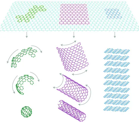
named graphene3. Graphene is only one atom thick, and it represents the basic
form of the other kinds of carbon systems described above. Graphite is formed by stacking of graphene layers, carbon nanotubes are rolled graphene sheets and fullerenes are cuts of graphene bulk in a form of a ball (see Fig. 1.1).
Figure 1.1: Diagram showing how graphene can be transformed into fullerenes, carbon nanotubes and graphite. Adapted from Ref. [5]
However pure two-dimensional systems were believed not to exist in nature, since it would be thermodynamically unfavorable [6], and it should bulk into some tri-dimensional form 4. Some efforts have been previously made to
pro-duce graphene, but only in 2004 it was possible for the first time to identify and measure this one-atom thick material [8, 9]. Since then, graphene turns out to be also a very exciting material, since it shows an unusual quantum Hall effect [10, 11], can sustain very high electrical currents without deterioration, is also one
3In the sp-2 configuration, the 2s and two 2p orbitals mix to form three in plane covalent
bonds. Each carbon atom has three nearest neighbors, forming a hexagonal planar network of graphene.
4In fact it was experimentally proposed that freely suspendended graphene has ripples [7],
1.1 Why study graphene? 7
of the materials with high young modulus, its electrons move through large dis-tances (few microns) without dissipation (for a review of these properties see Refs. [5, 12]). Also the electron dispersion is described by the Dirac equation, where the electrons have no mass [13]. Therefore, for the first time, it is possible to engineer relativistic quantum phenomena in a table-top experiment [10, 11, 14, 13].
Most of the graphene applications euphoria is due to its capacity of integra-tion with electronic circuits. Graphene has one the largest electron mobilities at room temperature, and much effort has been done to improve this property. Large mobility means less dissipation in the form of heat giving rise to fast electronic devices. Unlike semiconducting nanotubes, graphene is metallic, and, in principle, it is unlikely that grapene can act as a field effect transistor with high ON/OFF ratios. However, gap opening can occur by confinement of the electron wavefunc-tion in one direcwavefunc-tion, like in graphene nanoribbons [15, 16, 17], or by chemical modification of graphene.
Graphene nanoribbons present very interesting phenomena, where physical properties like electronic structure and spin transport depend on the width and geometrical structures of the edges [15, 16, 17]. However, unlike carbon nanotubes, which exhibit metallic or semiconducting behavior, graphene nanoribbons are ex-pected to show only a semiconducting behavior [17]. This is a good property for transistor applications, where the existence of a gap is desirable. Moreover, the edges of the nanoribbons can be chemically modified in order to change their physical properties. In another approach, chemical modification of graphene like hydrogenation (the so-called graphane) has been done [18], showing a possible gap in the electronic structure.
Bilayer graphene also exhibit many interesting phenomena. However, bilayer graphene does not exhibit a linear electronic dispersion. Instead, its electronic dispersion is described by a zero gap parabolic equation [13]. Moreover, bilayer graphene shows a different type of quantum Hall effect [19] and one the most striking features of bilayer is the fact that a gap can be opened by applying a perpendicular electric field [20, 21, 22, 23, 24], and this gap can be tuned by the strength of this electric field.
this sample preparation method is difficult to be integrated into a production line. Large scale methods like ultrasonification of graphite in solvents [25, 26] and epi-taxial growth on Ni [27] or silicon carbide surfaces have been successfully reported recently [28, 29, 30]. Although the electronic properties of these types of graphene samples are not so good and less uniform as compared to exfoliated graphene, these methods present important steps towards industrialization of graphene. Figure 1.2 shows four different types of graphene samples prepared by different techniques.
(a) (b)
(c) (d)
Figure 1.2: (a) Mechanical exfoliated graphene. (b) Suspension of graphene obtained by ultrasonification of graphite and a spray coating in the flexible substrate of the same graphene suspension. (c) Graphene grown in nickel and transferred to silicon oxide substrate. (d) Graphene islands grown in silicon carbide substrate. Adapted from Ref. [12]
Graphene already has given important contributions to nanoscience, present-ing many new physical properties and potential applications [5, 12]. However, progress for industrial applications of graphene are still in a very early stage, and the research on this novel material is important to determine its applicability.
1.2
Why study graphene with Raman spectroscopy?
1.2 Why study graphene with Raman spectroscopy? 9
lights with different frequencies from the frequency of the incident light on liquids. Since then, Raman spectroscopy has grown with the condensed matter research, and experiments are now relatively simple to be performed.
Raman spectroscopy has historically played an important role in the structural characterization of carbon materials [32, 33]. It has been used in the last decades to characterize graphite, carbon nanotubes, nanographite, amorphous carbon and, more recently, graphene. The Raman spectra for these different kinds of carbon materials are different from each other as shown Fig. 1.3. Although the main Raman bands can be observed in the spectra in every graphitic form, their shape, position and intensity are different. For example the G band around 1600 cm−1 in
Fig. 1.3 is a single peak for graphene and graphite, but for SWNT the G band is composed by two peaks.
Raman spectroscopy in graphite has been used to probe the degree of disorder, making possible to evaluate crystalline size along the plane and also to measure the degree of stacking order of the graphene layers [34, 35, 36]. In carbon nan-otubes, Raman spectroscopy has been intensively used to characterize their diam-eters, environmental effects, defects and optical transition energies [37]. The first Raman spectroscopy experiments in graphene came in 2006, when it was shown that Raman spectroscopy provides the perfect tool for determining the number of graphene layers (from 1 to 5 layers) [38, 39, 40]. Beyond that, Raman spectra of graphene provided a better knowledge about charge effects in the phonon energies [41, 42, 43, 44] as well as an experimental tool to estimate and monitor doping in graphene [45]. In Fig. 1.4 (a) we show the use of Raman spectroscopy to probe the number of layers and Fig. 1.4 (b) shows how it is possible to monitor the frequency of the Raman band as a function of the charge density in graphene. Moreover, due to the specific electron dispersion of graphene near the Dirac point, the vibrational and electronic structures of graphene systems were probed with the use of resonant Raman spectroscopy [46, 47], providing experimental support for understanding the vibrational and electronic properties of carbon materials.
Raman spectroscopy in graphene still has a wide variety of applications to be discovered. New physical phenomena are constantly being reported, such as electron and phonon properties [49], strain effects [50, 51], doping [52, 53, 54] and magnetic effects [55].
Figure 1.3: Raman spectra for different kinds of carbon systems, from top to bot-tom: graphene, HOPG, single wall carbon nanotubes (SWNT), damaged graphene, single wall carbon nano horn (SWNH) and amorphous carbon. The name for the main Raman bands are named in the figure, and are dis-cussed along the thesis.
in particular, by resonant Raman spectroscopy.
1.3
Outline
1.3 Outline 11
(a) (b)
Figure 1.4: (a) Raman spectrum of graphene layers, where it is possible to distinguish the shape of the Raman spectrum as a function of the number of layers [38]. (b) Raman frequency of a monolayer graphene G band as a function of charge concentration in the sample, showing that is possible to correlate the amount of doping with the frequency of the G band of graphene [45]. From Ref. [48]
Raman spectroscopy to distinguish a monolayer from few-layer graphene stacked in the Bernal (AB) configuration. In Chapter 4 we give the experimental details on sample preparation and the Raman instrument used in this work.
In Chapter 5 we derive the symmetry properties for N-layer graphene, where N is an integer, and give the selection rules for optical absorption and for first- and second-order Raman scattering processes. In Chapter 6 we show how the resonant Raman spectroscopy can be used in graphene systems to gather information about its electronic and vibrational properties. In Chapter 7 we make use of Raman spectroscopy to study electron-phonon interactions in bilayer graphene by applying a variable gate voltage between the graphene and the substrate. Finally, in Chapter 8 we draw the conclusions about this PhD thesis.
Chapter 2
Basic concepts of graphene
2.1
The
N
-layer graphene crystal
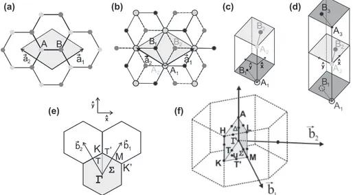
Graphene consists of an sp2 carbon hexagonal network, in which strong
co-valent bonds are formed between two adjacent carbon atoms. The unit cell for monolayer graphene (1-LG) contains two carbon atoms, A and B, each forming a triangular 2D network, but displaced from each other as shown in Fig. 2.1(a).
The primitive vectors a1 and a2 in Fig. 2.1 (a) can be written in terms of the lattice parametera as [33]:
a1 =
a 2(
√
3ˆx+ ˆy),a2 =
a 2(−
√
3ˆx+ ˆy). (2.1)
The value of the lattice parameter is a = 2.46 ˚A, which is considered to be the same as in graphite and is derived from the carbon-carbon distance of 1.42 ˚A [33]. The direction ˆx and ˆyare along the vertical and horizontal directions of Fig. 2.1 (a), respectively. The first Brillouin zone in graphene, shown in Fig.2.1(e), is hexagonal and its reciprocal vectors b1 and b2 [33] are given by:
b1 =
2π a (
√
3
3 kˆx+ ˆky),b2 = 2π
a (
−√3
3 ˆkx+ ˆky). (2.2)
Figure 2.1: (a) The top view of the real space unit cell of monolayer graphene showing the inequivalent atoms A and B and unit vectors a1 and a2. (b) The top
view of the real space of bilayer graphene. The light/dark gray dots and black circles/dots represent the carbon atoms in the upper and lower layers, respectively, of 2-LG. (c) The unit cell and the ˆx and ˆy unit vectors of the bilayer and (d) trilayer graphene. (e) The reciprocal space unit cell showing the 1st Brillouin zone with its high symmetry points and lines, such as T
connecting Γ to K; Σ connecting Γ to M; and T′ connecting K toM. The two primitive vectors on the top of the three hexagons shows the real space coordinate axes. (f) The Brillouin zone for 3D graphite, showing the high symmetry points and axes.
The 3D graphite structure corresponds to a stacking of graphene layers in the direction perpendicular to the basal plane (c-axis) in an AB (or Bernal) stacking arrangement, in which the vacant centers of the hexagons in one layer have carbon atoms in hexagonal corner sites of the two adjacent graphene layers, as shown in Fig. 2.1(b). In graphite with AB stacking, the unit cell consists of four carbon atomsA1,A2, B1, and B2. Normally, the bilayer graphene samples obtained from
the mechanical exfoliation of graphite exhibit an AB stacking arrangement, and therefore the unit cell of bilayer graphene (2-LG) has the same number of atoms as that for graphite, with four atoms per unit cell, as shown in Figs. 2.1(b) and 2.1(c). Trilayer graphene (3-LG) in turn contains three layers, two of which are like bilayer graphene and the third layer has atom A3 over A1 and atom B3 over
B1 as shown in Fig. 2.1(d). Four layer graphene (4-LG) consists of the stacking
2.2 Band structure of N-layer graphene 15
Table 2.1: The coordinates of the high symmetry points for the first Brillouin zone of graphene
Point Coordinate
Γ (0,0,0)
K (0,4π
3a,0) K′ (0,-4π
3a,0) M ( 2π
√
3a,0,0)
The first Brillouin zone of these two-dimensional structures is shown in Fig. 2.1(e). On the other hand, the graphite which has a third direction along thez axis has a three-dimensional Brillouin zone which is shown in Fig. 2.1(f) along with its high symmetry points and lines.
2.2
Band structure of
N
-layer graphene
2.2.1 Monolayer graphene
In graphene or graphite, the atomic orbitals are in asp2hybridization, in which the carbon atoms are bounded covalently to each other forming a 120◦ angle. In
this kind of hybridization, the π electrons along the z (out of plane) direction are related to many interesting physical phenomena, since they have lower energy compared to theσ orbitals.
The electronic structure of monolayer graphene (1-LG) can be calculated from a variety of ways, from tight binding based approach [33, 56] to ab-initio methods. We can construct the tight binding Hamiltonian following Ref.[56] as:
Hmonolayer = µ
0 γ0f(k)
γ0f∗(k) 0
¶
. (2.3)
where f(k) =e(ikx√a3)
+ 2e(−ikx2√a3)
cos(kya2). The eigen energies are found by di-agonalizing this Hamiltonian, and it is important to note that here we ignore the overlap integral matrix S as given in Ref. [33]. The γ0 parameter is the nearest
neighbor transfer integral between the atomic orbitals of the carbon atoms A and B of the graphene sheet.
is a zero gap semiconductor, where the valence and conduction bands touch each other at the K (or Dirac) point [56]. For points around the K point, the electronic structure can be described as a linear dispersion (see the right side of Fig. 2.2 (a)), orE(k) = √23γ0ak=~vFk[33]. This expression relates directly the electron wave vector k with the energy by a Fermi velocity vF, which is found to be close to 106 m/s [10] (or γ
0 ≈3.0 eV). Fig. 2.2 shows the energy contours around
the K point where is possible to clearly observe that, as the energy increases, the circular form tends to be trigonal due to the symmetry of the lattice, and this is called trigonal warping effect. Beyond the tight binding approach, the monolayer band structure can also be evaluated by ab-initio methods which do not depend on the number of neighbors included. Fig.2.2(c) shows the electronic structure of monolayer graphene along the high symmetry lines calculated via density functional theory (DFT) [53].
2.2.2 Bilayer graphene
The bilayer graphene is also a zero gap semiconductor but the electronic dis-persion is no longer linear around the K point, but it has a parabolic dependence withk [56]. Now, the first neighbor tight binding 4x4 Hamiltonian can be written as [33, 56]:
Hbilayer =
0 γ0f(k) γ1 γ4f∗(k)
γ0f∗(k) 0 γ4f∗(k) γ3f(k)
γ1 γ4f(k) 0 γ0f∗(k)
γ4f(k) γ3f∗(k) γ0f(k) 0
. (2.4)
Instead of only one tight binding parameterγ0, the bilayer has also theγ1, γ3
andγ4 parameters which are interlayer interactions between the nearest neighbors
atomic orbitals. Figure 2.3 shows the atomic structure of bilayer graphene, and the nearest neighbors in plane and out-of-plane tight binding parameters.
The calculated band structure of bilayer graphene obtained by diagonalizing
Hbilayer is shown Fig. 2.4 (a). Instead of one valence and one conduction bands as in monolayer graphene, the bilayer graphene has two valence and two conduction bands, where two of them touch each other at the K point and the other two are separated by 2γ1. Also the linear dispersion of monolayer graphene near the K
2.2 Band structure of N-layer graphene 17
K
M
G
K
G
M
K
(a)
(b)
(c)
Figure 2.2: (a) The electronic structure of monolayer graphene within the first Brillouin zone and, on the right, a zoom near the K point showing the linear dispersion. (b) Contour plot of the band structure near the K point. (c) Electronic structure of monolayer graphene along the high symmetry lines calculated via DFT [57].
Fig. 2.4(b) the DFT calculation along the high symmetry lines is also shown.
It is important to discriminate the influence of the γ3 and γ4 parameters on
the band structure of bilayer graphene. The γ3 parameter gives rise a trigonal
warping effect in the low energy spectrum as shown in Fig. 2.5 (a) [21]. This figure shows the contour plot near the K point for energies between 0 and 0.01 eV. It is clear in Fig. 2.5(a) that the equienergies curves are indeed triangles with opposite directions if compared to the crystal symmetry trigonal warping as show in Fig. 2.2(b). The γ4 parameter is related to the electron-hole asymmetry in
bilayer graphene [56]. In Fig. 2.5(b) the blue curve is calculated by settingγ4 = 0
and the red curve by γ4 6= 0, and we can see that now the conduction band of the
Figure 2.3: Atomic structure of bilayer graphene, where the overlap γ parameters are shown with the respective pair of atoms for eachγi interaction.
2.2.3 Band structure evolution to graphite
By stacking N graphene layers in the AB stacking arrangement the band structure continues to evolve with increasing number of atoms in the unit cell. Then the electronic bands starts to split into 2N components, i.e. trilayer graphene has three conduction and three valence bands and so on. Also the number of tight binding parameters between the neighbor atoms starts to increase with interactions between the first and third layer for example.
For graphite, the electronic structure can be described by the phenomenolog-ical Slonczewski-Weiss-McClure (SWM) model [1, 2]. In this model there are the same tight binding parameters as in bilayer graphene with the addition of two terms γ2 and γ5 which are the interactions between second-neighbor layers. This
model generates the electronic structure of graphite, which happens to be parabolic near the K point along the ΓK plane and linear near H point along the AH plane.
The SWM model can be also used to calculate the electronic spectrum of bilayer graphene, since it has the same number of atoms as in the unit cell and graphite [46]. However, for bilayer the interlayer interaction between the second-neighbor layers is ignored as we will show in Chapter 6.
2.3
Phonon structure of graphene
2.3.1 Phonons including the electron-phonon coupling
2.3 Phonon structure of graphene 19
K
(a)
(b)
Figure 2.4: (a) The electronic structure of bilayer graphene within the first Brillouin zone and, on the right, a zoom near the K point showing parabolic dispersion. (b) Electronic structure of bilayer graphene along the high symmetry lines calculated via DFT [57].
(b)
(a)
K
G
M
K
G
M
Figure 2.5: (a) Contour plot of the band structure near the K point. (b) Electronic structure of bilayer graphene along the high symmetry lines forγ4= 0 (blue
lines) and γ4 = 0.15 eV (red lines).
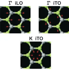
Near the zone center (Γ point), the in-plane iTO and iLO optic modes corre-spond to the vibrations of the sublattice A against the sublattice B as shown in Fig. 2.7, and these modes are degenerate at the Γ point. According to group theory, the degenerate zone-center iLO and iTO phonon modes belong to the two-dimensional E2g representation and, therefore, they are Raman active modes.[60, 33] The de-generacy of the iLO and iTO phonons disappears for general points inside the first Brillouin zone (BZ) of graphene. The phonon modes around the K point are especially important, since theD-band and G′-band are related to phonon modes
in the vicinity of the K point as will be discussed later. Exactly at the K-point, the phonon which comes from the iTO branch is non degenerate and belongs to the A′
1 irreducible representation of the point group D3h, and the eigenvector of
2.4 Phonons corrected by the electron-phonon coupling 21 0 400 800 1200 1600 F r e q u e n c y ( c m -1 ) W avevector F
M K F oTO oTA iTA iLA iLO iTO 0 0.02 DOS (state/cm -1 /atom)
Figure 2.6: Calculated phonon dispersion relation of graphene. [58] LO, iTO, oTO, LA, iTA and oTO are phonon modes at the Γ point. The green circles are X-ray scattering measurements from Ref. [59]. On the right the DOS of the phonons.
2.4
Phonons corrected by the electron-phonon
coupling
2.4.1 The electron-phonon interaction and Kohn anomaly
In a first approximation the lattice vibrations are determined by the vibration of the ions with respect to its equilibrium position. In the particular case of graphene, one should include the electronic cloud which should also affect the movement of the ions. When the local density of electrons is increased, an extra kinetic energy should appear due to exclusion principle, and thus the electronic cloud screens the atomic vibrations [62]. The effect of mutual interaction between the electronic cloud and the atomic motion is called electron-phonon interaction.
The electron-phonon interaction affects the phonon spectrum and, to calculate this change we shall use pertubation theory for the electron-phonon Hamiltonian
G
iLOG
iTOK iTO
Figure 2.7: Eigenvectors for three phonon modes at Γ and K point in graphene.
ε=ε0+hΦk|He−p|Φki+hΦk′|H
e−pHe−p ε0−ε1 |
Φki+O3, (2.5)
whereε0 and ε1 are the unperturbed and perturbed energies of the state Φk which has nq phonons in the mode q and nk electrons in the state k. Then the state is written as Φk = |nq, nki. The first-order therm vanishes because He−p either creates or destroys a phonon and the resulting wavefunction is orthogonal to Φk. The second-order contribution can be written as (see Appendix A):
ε2 =hΦk′|
X
k,k′
|Mkk′|2
"
a†−qc†kck′a−qc†k′ck
ε0−ε1
+aqc
†
kck′a†qc†k′ck
ε0−ε1
#
|Φki, (2.6)
wherea†
q(aq) creates (destroys) a phonon at the stateq,c†q(cq) creates (destroys) an electron in the statek, andMkk′ are the electron-phonon matrix elements. The
first therm in the brackets represents an electron being scattered from k to k′ by absorbing a phonon with wavenumberq=k−k′. The first denominator (ε0−ε1)
2.4 Phonons corrected by the electron-phonon coupling 23
Figure 2.8: Feynman diagram for the second-order process that re-normalizes the phonon energy. The first node shows the decay of a phonon into an electron-hole pair, and the second node shows the recombination of the electron hole and the emission of a phonon.
(see Appendix A) in terms of occupation numbers for electrons (hnki) and phonons (hnqi), and we find that the corrected phonon energy ~ωq(p) is [62]:
~ω(p)
q =~ωq+ X
k
|Mkk′|2
2hnki(εk−εk′)
(εk−εk′)2−(~ωq)2
. (2.7)
This equation relates the phonon frequency change due to electron-phonon interaction. Fig. 2.8 shows the diagram related to Eq. 2.7 in which an electron in the valence band is first excited to the conduction band by absorbing a phonon, thus creating an electron-hole pair. The diagram shown in Fig. 2.8 is valid for the first term of Eq. 2.6. The electron and hole then recombine, thus emitting a phonon. Both the frequency and lifetime of the phonon are significantly affected by this second-order process [42, 63, 64].
Now let’s assume that the electronic energy is much larger than the phonon frequency then we have that:
~ωq(p) =~ωq−X k
|Mkk′|2
2hnki (εk′ −εk)
. (2.8)
This less generic equation is useful to see the consequence when we take its derivative with respect to q(assuming a one-direction derivative for clarity) [62]:
~∂ωq(p) ∂qx
=~∂ωq ∂qx −
X
k
|Mkk′|2
2hnki (εk−qx−εk)2
∂ε(k−qx) ∂qx
An interesting behavior occurs whenq= 2kF, wherekF is the radius of the Fermi surface. The statesk′ =k−q andk are connected by qin the same Fermi surface.
Then, the summation in Eq. 2.9 contain divergent factors because εk−qx will be equal to εk when q connects states in the same Fermi surface. This divergency is the so-called Kohn anomaly [65] which appears as a kink in the phonon spectrum whenever q = 2kF. Or, more generally, the Kohn anomaly occurs when q = k1−k2 +b where k1 and k2 are electron state at the Fermi surface and b is a reciprocal lattice vector, necessary to bring the phonon wavevectorqback into the 1st Brillouin zone [65].
In the case of graphene the Fermi surface corresponds to the K and K′ points,
and then the Fermi wavevectors k1 and k2 are at the corners of the 1st Brillouin zone (namely theK and K′ vectors) and, as first reported by Piscanec et al. [66], the Kohn anomaly occurs for special phonons at the Γ and K points of graphene. In particular, it was shown in this work [66] that the slopes of the phonon dispersion at these special points are proportional to the electron-phonon coupling parameter λe−p.
Figure 2.9 shows the calculation performed by Piscanecet al. [66] where its is possible to observe the divergent characteristic of the Kohn anommaly near the Γ point for the iLO mode and at K point for the iTO mode.
2.4.2 Non-adiabatic effects of the phonon frequency
2.4.2.1 Monolayer graphene
The adiabatic approximation is one of the most useful methods to facilitate quantum mechanical calculations of solids or molecules. One of the most important features of this approximation (first introduced by Born and Oppenheimer), is the separation of variables between the electronic and nuclear variables [67]. With this approximation we are led to the adiabatic criterion [67]:
~ωq ≪ |εk−εk′|, (2.10)
and this condition is well satisfied for some semiconductors and insulators. How-ever, for metallic systems the adiabatic criterion is broken as we have ~ωq ∼
|εk−εk′| [67]. In the previous section, from equation 2.7 to 2.8 we assumed that
2.4 Phonons corrected by the electron-phonon coupling 25
Figure 2.9: Phonon dispersion of graphene from Ref. [66] showing the Kohn anomaly at the Γ and K points. The lines of the top part of the figure is the theoretical calculated curve and the symbols are experimental data. The both bottom figures are a closeup of the phonon dispersion near the Γ and K points. The different lines shows different parameters for the theoretical calculation done in Ref [66].
for metals and graphene. Now we should study the dependence of the phonon fre-quency as a function of the Fermi energy in the framework of non-adiabatic second order pertubation theory of the Fr¨ohlich Hamiltonian. We can rewrite Eq. 2.7 in terms of the Fermi-Dirac distribution instead of the electron occupation number, i.e.,
~ω(p)
q =~ωq+ Z
kdk|Mkk′|2
2(εk−εk′)
(εk−εk′)2−(~ωq+iδ)2×
à 1
e εk′ −EF
KB T + 1
− 1
e εk−EF
KB T + 1 !
,
(2.11)
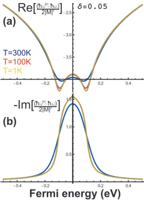
For monolayer graphene we assume the linear electronic dispersion (E(k) = vFk), and than we calculate the frequency shift for the phonon at q = 0 in units of the electron-phonon coupling as a function of the Fermi energy (EF)(See Fig. 2.11 (a)). The phonon frequency has a logaritimic divergence atωq/2. The renor-malization of the phonon energy is strongly dependent on the Fermi level position, which can be tuned by doping graphene with electrons or holes. In fact, if one changes the Fermi energy of the system, there is a reduction in the interaction be-tween phonons and interband electron-hole pairs, thus changing the effective force constant of the lattice vibrations. This renormalization, which is very effective when |EF|<~ω0/2, is inhibited when the change in the Fermi level is larger than
half of the phonon energy, as shown in Fig. 2.11. This is explained by the fact that the Pauli exclusion principle in this case suppresses the process depicted in Fig 2.8 (creation of an electron-hole pair by exciting a phonon). The suppression of the renormalization due to the electron-phonon interaction can be seen also in the lifetime of the phonon which is large when |EF| < ~ω0/2 (see Fig. 2.11 (b)).
The temperature also strongly affects the anomaly in ~ω0/2, which is smoothed as can be seen in the frequency and lifetime calculation shown Fig. 2.11 for three different temperatures.
Theoretical models for the phonon self-energy [42, 63, 64] and time dependent second order pertubation theory have predicted the same logarithmic dependence for the phonon softening on the chemical potential (or Fermi level change) for graphene. This anomalous phonon behavior has been experimentally observed by Raman spectroscopy of doped graphene [43, 44, 45], as shown in Fig. 1.4 (b).
2.4.2.2 Bilayer graphene
In the case of bilayer graphene, the phonon mode at q = 0 splits into two components, associated with the symmetric (S) and anti-symmetric (AS) displace-ments of the atoms in the two layers. Moreover, due to the splitting of the π and π∗ bands in this material, phonons can couple with electron-hole pairs produced
2.4 Phonons corrected by the electron-phonon coupling 27
(hw -hw) 2|M|2
(p)
Re[
]
Fermi energy (eV)
(hw -hw) 2|M|2
(p)
-Im[
]
d=0.05
T=300K
T=100K T=1K
(a)
(b)
Figure 2.11: The renormalization of the phonon energy associated with the mechanism shown in Fig. 2.8 is allowed when the change in the Fermi energy ∆εF
is smaller than half of the phonon energy ~ωG/2 (upper figure) and it is
suppressed for ∆εF >~ωG/2 (lower figure).
In order to discuss the phonon renormalization effect in bilayer graphene, we must consider the selection rules for the interaction of the symmetric and anti-symmetric phonons with the interband or intraband electron-hole pairs. The band structure of bilayer graphene near the K point shown in Figure 2.12 consists of four parabolic bands, two of them touching each other at the K point, while the other two bands are separated by 2γ1, where γ1 ∼0.35 eV.
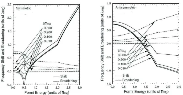
The electron-phonon interaction in bilayer graphene is described by a 2x2 ma-trix for each phonon symmetry, where each mama-trix element gives the contribution of electron-hole pairs involving different electronic sub-bands [68]. For the symmet-ric phonon mode, all matrix elements are different from zero, and this phonon can interact with both interband or intraband electron-hole pairs, as shown in Figure 2.12(a), giving rise to the phonon energy renormalization. However, for the anti-symmetric phonon mode, the diagonal terms of the matrix are null, showing that there is no coupling between the AS phonons and interband electron-hole pairs. Therefore, no Kohn anomaly is expected for the antisymmetric phonon mode when the Fermi level is at the Dirac point.
2.4 Phonons corrected by the electron-phonon coupling 29
Figure 2.12: Parabolic band structure of bilayer graphene near theK point. The verti-cal arrows illustrate the possible transitions induced by symmetric (green) and antisymmetric (red)q=0 phonons for (a) interband electron-hole pairs creation at (εF=0) and (b) intraband electron-hole pairs creation (εF <0).
The opening of an energy gap around the Dirac point is not considered in this diagram.
Dirac point, [for instance,εF <0 as shown in Fig. 2.12(b)], the intraband electron-hole pairs can be produced by phonons. In this case, the anti-symmetric phonons also have their energies renormalized, giving rise to the Kohn anomaly. Notice that, since the energy separation between the π1 and π2 bands (γ1 ∼ 0.35 eV) is larger
than theGband energy (∼0.2 eV), the electron-hole pair creation process by those phonons is a virtual process. Therefore, we expect the dependence of the shift of the anti-symmetric mode with Fermi energy to be smoother than that of the symmetric mode. A similar result has been recently observed in gated semiconducting carbon nanotubes [69] which had a band gap larger than the phonon energy.
Figure 2.13: Calculated frequency shift (closed lines) and broadening (dashed lines) for the symmetric mode (left panel) and anti-symmetric mode (right panel) of bilayer graphene as a function of the Fermi energy for different values of δ. Adapted from Ref. [68]
Chapter 3
Basic concepts of Raman
scattering
3.1
Theory of Raman scattering
3.1.1 Light-matter interaction
The interaction of light and matter is of great interest due its contribution to many physical phenomena, such as light scattering (Raman and Rayleigh), absorption and luminescence. We begin the calculation of light absorption of an electron (with charge−e) on a generic crystal with the Shr¨odinger equation given by [70]:
[((pˆ+eA)
2
2m ) +Vcrystal]Φ(r, t) =i~
∂Φ(r, t)
∂t , (3.1)
where A is the vector potential and Vcrystal is the potential of the crystal under study. By expanding the quadratic term we have:
[pˆ
2
2m +Vcrystal]Φ(r, t) +
[epˆ·A+eA·ˆp+eA2]
2m Φ(r, t) =i~
∂Φ(r, t)
∂t . (3.2)
approximation, we can neglect the quadratic term A2 when we are using ordinary light sources [70, 71]. The operator ˆp·A acting on a wavefunction Φ in Eq. 3.2 can be written as [70]:
ˆ
p·AΦ = −i~∇ ·(AΦ) =−i~[(∇ ·A)Φ +A·(∇Φ)]. (3.3)
By using the Coulomb gauge we have that ∇ · A = 0, then we are left with HI = (e/m)A·ˆp. The second approximation is to note that the magnetic field contribution for the interaction of electrons with the electromagnetic wave is much smaller than that for the electric field [70]. With this simplification we can write the vector potentialA in terms of the electric field by noting that in the Coulomb gauge we have the relationE=−∂∂At. Then by writing the electric field asE(r,t) = 2E0cos(kL·r−ωt)ˆe, wherekLis the wavevector of the electromagnetic wave andˆe is the polarization vector of the light, we are left with the light-matter perturbation written as [70]:
HI = eE0
imω[e
i(kL·r−ωt)
−e−i(kL·r−ωt)](ˆe·ˆp). (3.4)
The first term of the above equation gives rise to the electron absorption of a photon with energy ~ω and momentum ~kL, and the other term, to the emission of a photon due to the electron decay [70].
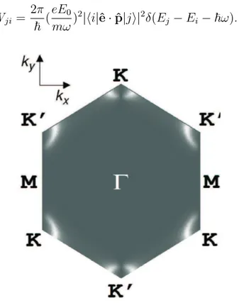
The Hamiltonian described by Eq. 3.4 when bracketed with initial and final electronic states with ki,e and kf,e wavevectors, lead to the momentum selection rule:
ki,e+kL=kf,e. (3.5)
By quantifying the values ofkL in terms ofki,e andkf,e in the first Brillouin zone, we can make the approximation that kL≪ki,e;kf,e. Therefore the selection rule for light absorption with wavevectors much smaller than the Brillouin zone of a crystal is: ki,e≃kf,e (Appendix B).
With this last approximation, we are led to the electric-dipole approximation, where we expand the exponential terms in Eq. 3.4 (e(ikL·r) = 1 + ik
3.1 Theory of Raman scattering 33
and keep only the first term. Now by using time-dependent perturbation theory [71, 72] for HI we are left with absorption transition rate from the state i to j (Fermi golden rule)[70, 72]:
Wji= 2π
~ ( eE0
mω)
2
¯ ¯ ¯ ¯
hi|ˆe·pˆ|ji Ej −Ei−~ω
¯ ¯ ¯ ¯
2
. (3.6)
This equation gives the probability of an electron with initial state i with energy Ei to absorb a photon with energy~ω going to a final statej with energyEj. We should note that when we are in the case of resonant exitation (Ej−Ei =~ω), we rewrite Eq. 3.6 as [72]:
Wji= 2π
~ ( eE0
mω)
2
|hi|ˆe·ˆp|ji|2δ(Ej −Ei−~ω). (3.7)
Figure 3.1: The calculated optical absorption intensity of graphene with light polariza-tion along ky direction, where it is possible to observe that the absorption is
zero for the vertical lines connecting K and K′ points. From Ref. [73]
that, due to the special linear dispersion of graphene, there is a node along the ΓK line when the incident light has polarization along theydirection. Figure 3.1 shows a plot of the optical absorption intensity in the first Brillouin zone where the the light polarization is along the ky direction in this figure. It is possible to observe an absorption node along the ΓK line in the ky direction. This effect has been experimentally observed by Can¸cado et al. in graphite edges [74] and graphene nanoribbons [75]. We will discuss later in Chapter 5 the application of Eq. 3.7 together with group theory in graphene, which gives the same result obtained by Gr¨uneis et al.. Also, this optical absorption node will be used in Chapter 5 to describe second-order Raman bands within a group theory approach.
3.1.2 Macroscopical approach to the Raman scattering and selection rules
The macroscopical approach to explain the Raman scattering is based on the action of an incident light on a extended medium creating a macroscopic polariza-tion vector [76]. To begin, consider an infinite medium with dielectric susceptibility χ, which is a tensor. The induced electric dipole can be written in terms of electric field E of the incident light on the medium as:
P=χ·E, (3.8)
where the electric field is written as a plane wave:
E=E0cos(k·r−ωt). (3.9)
Herek and ω are the wavevector and the frequency of the incident light.
3.1 Theory of Raman scattering 35
χij = (χij)0+
X l µ ∂χij ∂Ql ¶ 0
Ql+O(2), (3.10)
where (χij)0 is the value of χij in the equilibrium configuration. To first order, we can rewrite Eq. 3.8 as:
P=Prayleigh+Praman, (3.11)
where the Prayleigh is the polarization vector oscillating with same frequency as that of the incident radiation, and Praman is the modified polarization due to the vibration of the atoms. Combining Eqs. 3.8, 3.9 and 3.10, we have the Raman contribution to the induced polarization given by:
Praman,i = X i,j µ ∂χij ∂Ql ¶ 0
QlE0,jcos(k·r−ωt). (3.12)
In order to determine the frequency and wavevector of Praman we describe Ql as a plane wave with wavevector qand frequency ω0 as:
Ql=Q0lcos(q·r−ω0t)·e.ˆ (3.13)
Inserting the above equation into Eq. 6.2, and using the trigonometrical rela-tion of cosines, we find [76]:
Praman,i = 1 2 X i,j µ ∂χij ∂Ql ¶ 0
Q0lE0,j×{cos[(k+q)·r−(ω+ω0)t]+cos[(k−q)·r−(ω−ω0)t]}.
(3.14)
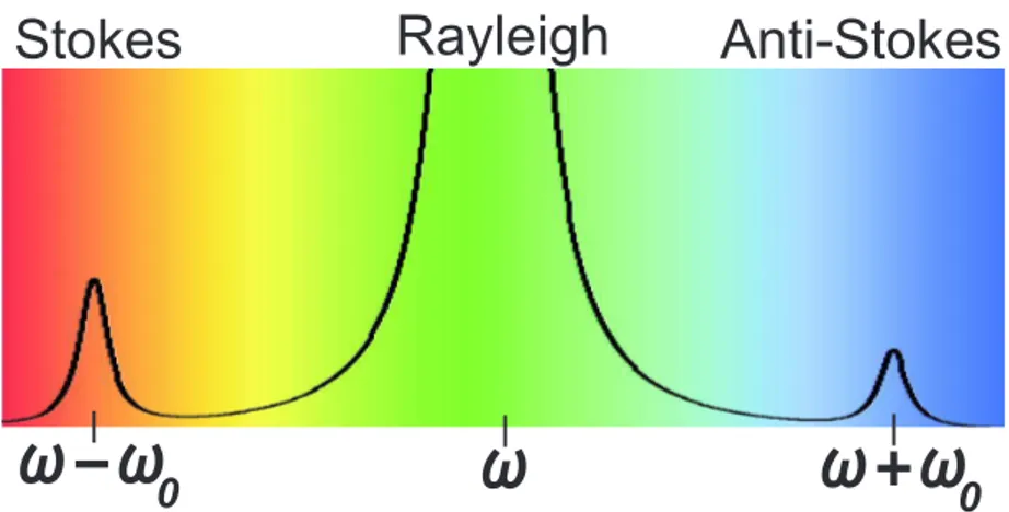
This final result shows that the modified polarization has two components, the first (second) with higher (lower) frequency with respect to the incident light. We call the Stokes component of the Raman scattering the scattered wave with wavevector kS = (k−q) and frequency ωS =ω−ω0, and the Anti-Stokes component which
Figure 3.2 illustrates a Raman spectrum in which an incident light with frequency ω creates Stokes and anti-Stokes components with frequency given by ω−ω0 and
ωi+ω0 respectively. Inserting Eq. 3.14 into Eq. 3.11, it is possible to observe that
an incident light with frequencyω will generate scattered light with frequenciesω (Rayleigh) and ω±ω0 (Raman), which is illustrated in Fig. 3.3.
w
w-w
0
w+w
0Stokes
Rayleigh
Anti-Stokes
Figure 3.2: Schematics of the Raman spectrum where an incident light with frequency
ω generates an elastically scattered light (Rayleigh) and two inelastically scattered components with frequency ωi −ω0 (Stokes) and ωi+ω0
(anti-Stokes).
Notice that due to the conservation of momentum for Stokes or anti-Stokes scattering we should analyze the magnitude for both incident and phonon wavevec-tors that contributes to the Raman scattering. Typically, light with wavelength in the visible range (500 nm) has a wavevector in the order of 107 m−1, which will create a maximum phonon wavevector with this order of magnitude. If we compare the magnitude ofqwith the dimensions of the first Brillouin zone which, typically, is in the order of 1010 m−1, we can see that visible light only probes phonons with
small wavevectors, and first order Raman is limited to analyze zone-center phonons (q∼0) [76].
To find the Raman selection rule, we note that polarizability derivative ∂χij ∂Qk in Eq. 3.14 is a second rank symmetric tensor [76, 77]. Then a phonon belonging to an specific irreducible representation is Raman active if it transforms as quadratic basis functions (e.g. x2,y2,z2,xy,xz and yz), which are found in character tables
in group theory text books [77].
3.1 Theory of Raman scattering 37
w
w
0
P
P
0P
ind{
w
w+w
0
w-w
0
Rayleigh
Raman
Figure 3.3: Schematics of an incident electromagnetic wave interacting with a material with a phonon frequencyω0, creating thus an scattered electromagnetic wave
with three frequency components, one associated with the Rayleigh scatter-ing and two with the Raman scatterscatter-ing.
Brillouin zone as in first order Raman. Expanding Eq. 3.10 to second order and then following the same steps as before we are led to :
P2raman ∝cos[(k+qa+qb)·r−(ω+ωa+ωb)t]
+ cos[(k+qa−qb)·r−(ω+ωa−ωb)t] (3.15) + cos[(k−qa+qb)·r−(ω−ωa+ωb)t]
+ cos[(k−qa−qb)·r−(ω−ωa−ωb)t], (3.16) (3.17)
can occur with the presence of a defect with wavevector d, and in this case the Raman selection rule is qa ±d ∼ 0. We are going to describe two-phonon and defect-induced Raman scattering in graphene in more details in Sec. 3.2.
3.1.3 Microscopical approach to the Raman scattering, selection rules and the resonant Raman scattering
We begin the quantum mechanical treatment of Raman scattering by illustrat-ing the Feynman diagram for a Stokes process in Fig. 3.4 (a) [76]. This diagram has three vertices, each one representing first-order time dependent pertubation in the system. The first vertex represents a initial state|ii of the system going to an excited state |ni due to electron-radiation interaction. In the second vertex, the state|niof the system goes to the state|n′idue to an electron-phonon interaction.
In the third and last vertex, there is a recombination of the electron-hole pair and the system goes to the final state |fi of the system. In the first vertex there is an absorption of a photon with energy ~ωi, in the second vertex there is an emission of a phonon with energy ~ωph and in the last vertex there is emission of a photon with energy ~ωS. We can define these four states of the system as:
|ii= |pi,0, pph, ψ0i,
|ni= |pi−1,0, pph, ψeni, (3.18)
|n′i= |pi−1,0, pph−1, ψn
′
e i, (3.19)
|fi= |pi−1,1, pph−1, ψ0i, (3.20)
where the four terms inside de brackets are the number of incident photons, number of scattered photons, number of phonons and the electronic state, respectively. The energies associated with these states are:
Ei = pi~ωi+pph~ωph+Ev,
En = (pi−1)~ωi+pph~ωph+Ecn, (3.21) En′ = (pi−1)~ωi+ (pph−1)~ωph+En
′
c , (3.22)
3.1 Theory of Raman scattering 39
where Ev and Ec is the energy of the valence and condution for example. The overall of the Raman process can be alternately viewed following the three steps in Fig. 3.4 (b). However the horizontal lines in this picture does not represent the electronic energy levels of the system.
w
i
w
sw
phn
n'
photon phonon electron-hole light-matter interaction electron-phonon interaction>
|i |f
>
>
|n>
|n'w
iw
sw
ph(a)
(b)
(1) (2) (3)
(1)
(2)
(3)
Figure 3.4: (a) Feynman diagram of the one-phonon Raman process. (b) Scheme of the Raman scattering depicted by the Feynman diagram. (The horizontal lines of part (b) do not correspond to the electronic levels, as discussed in the text).
To compute the Raman scattering probability of the process depicted in Fig. 3.4 (a) we start with the first vertex which contributes with a first order pertubation term (term inside the absorption probability in Eq. 3.6) in the form of [76]:
X
n
hn|Hlight|ii [~ωi−(En
c −Ev)]
. (3.24)
X
n,n′
hn′|H
el−ph|nihn|Hlight|ii [~ωi−(En
c −Ev)][~ωi −~ωph−(Ecn′ −Ev)]
. (3.25)
Finally we multiply this last equation to the third vertex, which contributes with the emission of a photon, then we have [76]:
X
n,n′
hf|Hlight|n′ihn′|Hel−ph|nihn|Hlight|ii [~ωi−(En
c −Ev)][~ωi−~ωph−(Ecn′−Ev)][~ωi−~ωph−~ωS]
. (3.26)
The term [~ωi−~ωph−~ωS] in the denominator gives the energy conservation rule of the Raman process and it should vanish. Then the Raman scattering probability can be written as [76]:
Praman = µ 2π ~ ¶¯ ¯ ¯ ¯ ¯ X n,n′
hi|Hlight|n′ihn′|Hel−ph|nihn|Hlight|ii [~ωi−(En
c −Ev)][~ωi −~ωph−(Ecn′ −Ev)] ¯ ¯ ¯ ¯ ¯ 2
δ(~ωi−~ωph−~ωS).
(3.27)
In fact Eq. 3.27 is not the complete scattering probability of the Raman process, because there are five more possible permutations of time order for each event in the diagram depicted in Fig. 3.4 (a). The complete calculation can be found in Ref. [76], but the most important contribution indeed comes from the above equation [76].
fi-3.1 Theory of Raman scattering 41
nal irreducible representation Γabsorption(Γemission) [77]. For the Hamiltonian of the electron-phonon coupling, the irreducible representation is the same as the phonon irreducible representation [78, 64]. Then the direct product of the electron-phonon irreducible representation and representation of the states |ni and hn|will creates a representation Γel−ph. Then the Raman probability will be different from zero if [77]:
Γabsorption ⊗Γel−ph⊗Γemission ⊂Γ1, (3.28)
where Γ1 is the totally symmetric representation. The use of group theory is very
useful to determine only the Raman activity. However a active Raman mode can only be observed depending on the strength of the electron-phonon coupling and resonance conditions [76].
The resonance condition for the Raman scattering is given by the denomina-tor of Eq. 3.27. The Raman probability is strongly enhanced when the energy difference between incident photon (~ωi) and the electron-hole energy (En
c −Ev) or between the scattered photon (~ωS = ~ωi −~ωph) and electron-hole energy (En′
c −Ev) is zero [76]. We call resonant Raman scattering (RRS) when Raman probability is enhanced due to a vanishing denominator of Eq. 3.27. RSS has been largely applied to study not only the phonon structure of materials but its electronic properties as well. In resonance conditions, we can replace the sum of the n states in Eq. 3.27 by only one term that connects directly one state |ai with a photon energy ~ωa. In this case to avoid a unphysical situation where the denominator vanishes, we include an imaginary termiΓa which is a damping con-stant due to the finite lifetime of the excitation. Then in resonance conditions Eq. 3.27 can be written as [76]:
Praman≈ µ
2π ~
¶ ¯ ¯ ¯ ¯
hi|Hlight|aiha|Hel−ph|aiha|Hlight|ii [Ea
c −~ωa−iΓa][Eca−~ωS−iΓa] ¯ ¯ ¯ ¯
2
3.2
First- and second-order Raman scattering in
graphene
3.2.1 The Raman spectra of monolayer graphene
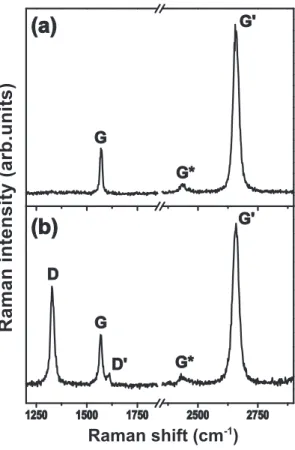
The most prominent features in the Raman spectra of monolayer graphene are the so-calledG band appearing at 1582 cm−1 and the G′ band (also called 2D
band in the literature [38]) at about 2700 cm−1 using laser excitation at 2.41 eV
(Fig. 3.5 (a)). There is also a low intensity peak near ∼2400 cm−1 which we call
here by G∗ band. In the case of a disordered or defective sample (Fig. 3.5 (b)), we
can also see the so-called disorder-inducedD-band, at about half of the frequency of the G′ band (around 1350 cm−1 using laser excitation at 2.41 eV). Additionally
to the D-band there is another weak disorder-induced feature which appears at
∼1620 cm−1 (D′ band).
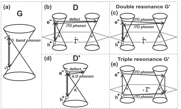
The G band is associated with the doubly degenerate (iTO and LO) phonon mode (E2g symmetry) at the BZ center. In fact, the G-band is the only band coming from a normal first order Raman scattering process in graphene systems. The process giving rise to the G-band can be viewed in Fig. 3.6 (a). On the other hand, the G′ and D-bands originate from a second-order process, involving two
iTO phonons near the K point for theG′ band or one iTO phonon and one defect
in the case of theD-band [79]. To further elucidate that the presence of defects is necessary for the observation of the D-band in the Raman spectra of graphene, we show in Fig. 3.7 a Raman mapping of the G and D bands in monolayer graphene sample in which defects had been created by focusing an ion beam (FIB) at six different positions. It is possible to observe on the right panel of Fig. 3.7 that the D band intensity is strong only where the FIB has created defects in the graphene.
Both theDandG′bands exhibit a dispersive behavior, i.e. their frequencies in
the Raman spectra changes as a function of the energy of the incident laser,Elaser.
The D-band frequency ωD upshifts with increasing Elaser in a linear way over a
wide laser energy range (including the visible range), the slope (∂ωD/∂Elaser) being
about 50 cm−1/eV. The slope of (∂ω
G′/∂Elaser) is about twice that of theD-band,
i.e., around 100 cm−1/eV [80, 81, 82].
The origin and the dispersive behavior in the frequency of the D and G′
3.2 First- and second-order Raman scattering in graphene 43
(a)
(b)
Figure 3.5: (a) Raman spectrum of adefect free monolayer graphene showing the main Raman features, theG,G∗andG′bands taken with a laser excitation energy of 2.41 eV. (b) Raman spectrum of a defective monolayer graphene sample, in which two disorder-induced Dand D′ Raman bands also appear.
wavevectorkmeasured from the K point absorbing a photon of energyElaser. The
electron is inelastically scattered by a phonon of wavevectorQand energyEphonon
to a point belonging to a circle around the K′ point, with momentum k′. The
electron scatters then back to the k state, and emits a photon by recombining with a hole. In the case of the Dband, the two scattering processes consist of one
elastic scattering event by defects of the crystal and oneinelastic scattering event by emitting or absorbing a phonon, as shown in Fig. 3.6. In the case of the G′
-band, both processes are inelastic scattering events involving two phonons. This double resonance mechanism is called an inter-valley process because it connects points in circles around inequivalent K and K′ points in the first Brillouin zone of graphene. On the other hand, the double resonance process responsible for the originates responsible for theD′ band (Fig. 3.6 (e)) is anintra-valleyprocess, since
(a)
(b)
(c)
(e)
(d)
Figure 3.6: (a) First-order Raman process which gives rise to the G band. One-phonon second-order Raman process giving rise to the (b)intervalley D band and (d) intravalley D′ band. (c) two-phonon second-order Raman spectral processes giving rise to the G′ band. (e) Schematic view of a possible triple resonance giving rise to the G′ Raman band in graphene.
point) [85].
The intervalley process depicted in Fig. 3.6 (b,c) can be alternatively viewed in Fig. 3.8, which shows an electron initially around the K point represented by the vector kmeasured from the K point being scattered by a phonon with wavevector Q, going to an intermediate state around the K′ point represented by k′. The
vectors uandu′ are the initial and intermediate electronic wavevectors, measured from the Γ point, and given by:
u=K+k
u′ =K′+k′ (3.30)
where K and K′ are the wavevectors of the K and K′ points respectively. The
3.2 First- and second-order Raman scattering in graphene 45
2 µm 2 µm
G band
D band
Figure 3.7: Raman mapping of a graphene sample in which defects have been created in six localized positions. The brightness in the color of the figure represents how intense is the Raman band over the sample. The left panel shows the mapping of the G band of monolayer graphene and a small part on the right due to fewlayer graphene. The right panel shows the D band mapping where it is possible to observe that the intensity is much greater at the six position in which defects were created. This Raman image was done by L. M. Malard with collaboration of B. Archanjo (Inmetro) and A. Jorio (UFMG).
Eq. 3.30 into the previous expression for Q, we have the phonon wavevector Q measured from the Γ point given by:
Q=K+k′−k, (3.31)
where we have used the fact that K′−K=K.
For convenience, we will work with the phonon vector q measured from the K point, which is related to the phonon wavevectorQ measured from the Γ point byq=Q−K(red shaded area in Fig. 3.8). The phonon vector qmeaured from the K point can be written only on terms of the initial and intermediate electronic wavevectors as:
From now on, we will use this notation for the phonon wavevector q written in terms of the initial k and intermediate k′ electron wavevectors, all of them measured from the K point.
K
K' u
k
u' k'
K Q
Q -k k' q
G
K
K
K'
Figure 3.8: The vectors u, u′ and Q represent the wavevectors of the initial electronic state, the intermediate electronic state and of the associated phonon, respec-tively, measured from the Γ point. The vectors k, k′ and q represent the
same states measured from the K point.
In principle, many different initial electronic states around the Dirac point and phonons with different symmetries and wavevectors can satisfy the double resonance (DR) condition. However, due to (1) the existence of singularities in the density of phonon states which satisfy the DR condition, (2) the angular de-pendence of the electron-phonon scattering matrix elements, and (3) destructive interference effects when the Raman transition probability is calculated, only a few specific DR processes contribute to the RamanG′andD bands [79, 47]. For exam-ple, only iTO and iLO branches are observed in the intervalley and intravalley DR processes, respectively, because the corresponding phonons are strongly coupled to electrons along the high-symmetry directions associated with the singularities in the DR phonon density of states [86].
WhenElaser is increased relative to the Dirac point, the resonancek vector for
![Figure 2.6: Calculated phonon dispersion relation of graphene. [58] LO, iTO, oTO, LA, iTA and oTO are phonon modes at the Γ point](https://thumb-eu.123doks.com/thumbv2/123dok_br/15742598.125749/29.918.242.647.189.493/figure-calculated-phonon-dispersion-relation-graphene-phonon-modes.webp)