Basic Reversible Logic Gates and It’s Qca Implementation
Papiya Biswas, Namit Gupta, Nilesh Patidar
Department of Electronics, SVITS, Baroli, Sanwer Road, Indore, India
Abstract
Reversible logic has various applications in various field like in Nanotechnology, quantum computing, Low power CMOS, Optical computing and DNA computing, etc. Quantum computation is One of the most important applications of the reversible logic.Basically reversible circuits do not lose information & reversible computation is performed only when system comprises of reversible gates. The reversible logic is design,main purposes are - decrease quantum cost, depth of the circuits & the number of garbage output. This paper provides the basic‘s of reversible logic gates & its implementation in qca.
Keywords
— Reversible logic, Fredkin gate, Feynman gate, Reversible gate, Power dissipation, Garbage, Quantum cost, Quantum-dot Cellular Automata, Reversible Computing.I. INTRODUCTION
In present day technology, in digital design ,energy loss is an important consideration. Traditional logic circuits are found ‗irreversible logic
circuit‘ & dissipate heat energy in an order KTln2 joules that the loss of per bit of information, where k(K=1.3806505*10-23JK-1) is Boltzmann‘s constant & T is absolute temperature. Bennett shows that in case of reversible logic computation KTln2 joules energy will not dissipate. Hence reversible logic design naturally gets priority to design combinational as well sequential circuit.Informations are not loss in reversible circuits.Reversible gates are required to design reversible circuits. Reversal gates are the building blocks for reversible circuits, having the following characteristics.
A reversible gate has equal input & output in order to have one to one mapping.So that the inputs of a reversible gate can be uniquely determined from its outputs. In a reversible gate fan out of every signal involving primary inputs must be one. Classical methods of synthesis of a logic cannot be directly applied to design reversible logic circuit. Garbage output is one of the most important features of a reversible gate . Every gate output that is not used as input to other gate or as a primary output is called garbage output. Each reversible gate is associated with a cost called quantum cost.The quantum cost of a reversible gate is the number of 2x2 reversible gates or quantum logic gates required in designing it.
II. BASIC DEFINATIONS RELATED TO REVERSIBLE LOGIC
A. Reversible Function:
The Boolean function F(y1; y2,...ym) with multiple output of m boolen variables is called reversible if the number of output is equal to number
of inputs.Every output pattern has a unique pre-image.
B. Reversible logic:
In reversible logic, the number of inputs are equal to number the outputs of the gates in order to have a one-to-one mapping. This generates a unique set of output vector for each set of input vector. This prevents the loss of information which causes power dissipation.In reversible logic fan-out is not possible and feedback or loops are not allowed.Some features of a reversible logic circuit that it should have are :- Minimum input constants.
Minimum number of reversible gates. Minimum number of garbage outputs.
C. Garbage outputs:
The number of outputs added to make an n-input-k-output function ((n;k)function)reversible is called garbage. whenever it is necessary to make equal number of inputs and outputs additional inputs or outputs can be added .Relation between the number of garbage outputs and constant inputs are shown below-
Input + constant input = output + garbage.
D. Quantum cost:
The cost of the circuit in terms of the cost of a primitive gate is called Quantum cost. It is calculated knowing the number of primitive reversible logic gates (1*1 or 2*2) required to realize the circuit. The quantum cost of a circuit is the minimum number of 2*2 unitary gates to represent the circuit keeping the output unchanged. Quantum cost of a 1*1 gate is 0 and 2*2 gate is the same, which is 1.
E. Flexibility:
The universality of a reversible logic gate for realizing more functions is term as Flexibility.
F. Gate Level:
Gate level refers to the number of levels in the circuit which are required to realize the given logic functions.
G .Width of reversible gate: The number is called logic width of the gate if the number of output bits of a reversible logic gate necessarily equals its number of input bits.
III. REVERSIBLE LOGIC GATES
There are three major design goals in reversible logic.1) The quantum cost, which is the number of 1*1 and 2*2 reversible calculations necessary to generate the logical output, should be minimized in order to reduce the computation complexity of the device.2) The delay,which is the logical depth of the device, should be minimized.3)The ancillary inputs and garbage outputs - inputs and outputs not implemented in the design of the gate and only serve to maintain reversibility of the device – ought to be reduced and ideally eliminated.
Some of the important reversible logic gates are:
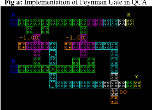
3.1Feynman Gate
The 2*2 gate is a feynman gate & is also called as controlled NOT , it is widely used for fan-out purposes. The inputs (A,B) and output P=A,Q=A xor B.
Fig 1: Feynman gate The Equations are:
P=A Q=A⨁
Table 1: Truth table of Feynman Gate Inputs Outputs
A B P Q
0 0 0 0
0 1 0 1
1 0 1 1
1 1 1 0
Fig a: Implementation of Feynman Gate in QCA
3.2 Fredkin Gate:The Fredkin gate is a 3*3 gate,
maps inputs(A,B,C)to outputs
(P=A,Q=A‘B+AC,R=AB+A'C) having quantum cost
of 5 and it requires two dotted rectangle.. Fredkin gate and its quantum implementations are shown below:
Fig2. Fredkin gate
Table 2 : Truth table of Fredkin Gate
Inputs Outputs
A B C P Q R
0 0 0 0 0 0
0 0 1 0 0 1
0 1 0 0 0 0
0 1 1 0 0 1
1 0 0 1 0 0
1 0 1 1 1 0
1 1 0 1 0 1
1 1 1 1 1 1
P=A A
B Q=A⨁
Feynman Gate
Q=A’B⨁
P=A
C A
B
Fredkin Gate
Fig b: Quantum implementation of Fredkin gate
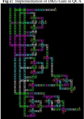
3.3 DKG Gate:DKG gate has 4 inputs and 4 outputs, so it is called Reversible 4*4 DKG gateBlock diagram & qca implememtation of. DKG gate with 4*4 inputs and outputs. Is shown below:
Fig3: Block diagram of DKG Gate
The equations are:
P = B Q = A C + AD
R = A⨁B C⨁D ⨁CD S = B⊕C⊕D
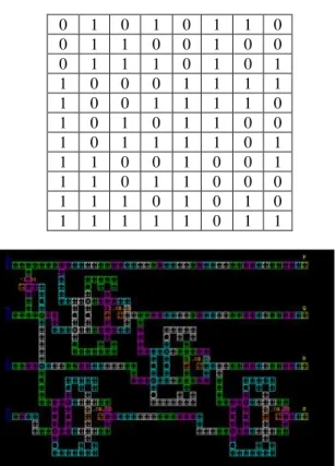
Table 3: Truth table of DKG Gate
Inputs Outputs
A B C D P Q R S
0 0 0 0 0 0 0 0
0 0 0 1 0 0 0 1
0 0 1 0 0 1 0 1
0 0 1 1 0 1 1 0
0 1 0 0 1 0 0 1
0 1 0 1 1 0 1 0
0 1 1 0 1 1 1 0
0 1 1 1 1 1 1 1
1 0 0 0 0 1 0 0
1 0 0 1 0 0 1 1
1 0 1 0 0 1 1 1
1 0 1 1 0 0 1 0
1 1 0 0 1 1 0 1
1 1 0 1 1 0 0 0
1 1 1 0 1 1 0 0
1 1 1 1 1 0 1 1
Fig c: Implementation of DKG Gate in QCA
3.4 MRG Gate: MRG is when utilized as a programmable reversible logic gate with two select inputs, it will calculate four logical calculations on those two logical outputs: OR,NOR, XOR and XNOR..Block diagram and qca implementation of MRG gate is shown below:
Fig4: Block diagram of MRG Gate
The equations are: P=A
Q = A⨁
�= ( ⨁ )⨁
S = (AB⨁ )⨁(( ⨁ )⨁ ))
Table4: Truth table of MRG Gate Inputs Outputs A B C D P Q R S 0 0 0 0 0 0 0 0 0 0 0 1 0 0 0 1 0 0 1 0 0 0 1 1 0 0 1 1 0 0 1 0 0 1 0 0 0 1 1 1 DKG
Gate A
B
C
D
P=B
Q
R
S= B⨁ ⊕
Q B
A
C
DP
R
S MRG
0 1 0 1 0 1 1 0 0 1 1 0 0 1 0 0 0 1 1 1 0 1 0 1 1 0 0 0 1 1 1 1 1 0 0 1 1 1 1 0 1 0 1 0 1 1 0 0 1 0 1 1 1 1 0 1 1 1 0 0 1 0 0 1 1 1 0 1 1 0 0 0 1 1 1 0 1 0 1 0 1 1 1 1 1 0 1 1
Fig d: Implementation of MRG Gate in QCA
IV.
Simulation Results:
All the design of basic reversible logic gates were verified by using QCA Designer tool ver.2.0.3.In the bistable approximation, we use the following parameters, which are default parameters in qca designer tool: number of samples(12800),convergence tolerance (0.001000), radius of effect(65.00nm), relativepermittivity (12.900000),clock high(9.800000e-022), clocklow (3.800000e-023),clock shift(0.000000+000),clock amplitude factor (2.000000), layer separation (11.500000), maximum iterations per sample (100). In our QCA layouts, we have the goal of workable design with compact layout. The simulation results of reversible logic gates are below:
Fig1:Simulation of Feynman Gate in QCA
Fig 2: Simulation of Fredkin Gate in QCA
Fig 3: Simulation of DKG Gate in QCA
Fig4:Simulation of MRG Gate in QCA
Table 5:Simulation parameters of some reversible logic gates based on QCA technology
Reversi ble gates
Comple xity (no.of cell)
Area(µ m^2)
Delay(c lock phases)
Simulati on time
Feynma n gate
75 0.08 1 3s
Fredkin gate
187 0.19 2 3s
DKG gate
752 1.24 4 6s
MRG gate
456 0.52 5 5s
V.
CONCLUSION:
design development using reversible logic circuits which are helpful in quantum computing, low power cmos, nanotechnology, cryptography, optical computing, and DNA computing, digital signal processing (DSP), quantum dot cellular automata, communication, and computer graphics.
VI.
ACKNOWLEDGMENT:
I acknowledge with sincerity and deep sense of gratitude,the invaluable guidance given by my guide Prof.Namit Gupta H.O.D of E.I Department and my co-guide Asso.Prof.Nilesh Patidar.I extend my sincere regards and heartfelt gratitude to my Parents and Family members for their support and encouragement.
REFERENCES
[1] E. Fredkin and T.Toffoli, ―Conservative logic,‖ in Collision-based computing, Springer-Verlag, 2002, pp. 47-81.
[2]. C.H.Bennet,‖logically reversibility of computation”, IBM journal of research and development pp 525-532, NOV 1973. [3]. ―A new reversible TSG gate and its
application for designing efficient adder circuit‖ by Himanshu Thapliyal and
M.B.Srinivas.
[4]. R. Feynman, "Simulating Physics with Computers," International Journal of Theoretical Physics, 1982.
[5] T. Toffoli, "Reversible Computing,"
Technical Report MIT/LCS/TM- 151, 1980. [6]. A. Peres, ―Reversible Logic and Quantum
Computers,” Physical Review, vol. 32, iss. 6, 1985, pp 3266-3276.
[7] R. Landauer, ―Irreversibility and Heat Generation in the Computational Process‖,
IBM Journal of Research and Development, 5, pp. 183-191, 1961.
[8] J.Smoline and David P.DiVincenzo, ―Five two-qubit gates are sufficient to implement the quantum fredkin gate‖, Physics Review
A, vol. 53, no.4, pp. 2855-2856, 1996. [9] H.R.Bhagyalakshmi, M.K.Venkatesha,‖
Optimized Reversible BCD adder using new Reversible Logic Gates‖, Journal of Computing, Vol 2, Issue 2, February 2010. [10] C. S. Lent, P. D. Tougaw, W. Porod, and G.
H. Bernstein, ―Quantum cellular automata,”
Nanotechnology, vol. 4, no. 1, pp. 49-57, January 1993.
[11] P. D. Tougaw and C. S. Lent, ―Dynamic behavior of quantum cellular automata,‖
Journal of Applied Physics, vol. 80 (8), 1996, pp. 4722–4736.
[12] W. Wang, R. Zhang, K. Walus, G. A.
Jullien, ―A method of majority logic
reduction for quantum cellular automata,‖
Nanotechnology, IEEE Transactions on, vol. 3(4), pp. 443–450, 2004.