*e-mail: [email protected]
1. Introduction
Transparent conduction oxides (TCO) exhibit good n-type conduction owing to their natural non-stoichiometry formed due to low formation energy of intrinsic donor defects, like structural metal ion interstitials (Mi) and oxygen ion vacancies (VO). TCOs are attractive in applications in advanced technology including lat panel displays and solar energy systems1. Therefore, it is necessary to seek ways to
improve their optoelectronic functions. One of these ways is a suitable doping, by which the carrier mobility (μel) and conductivity (σ) are improved without much reduction in transparency.
CdO is one of the TCOs of conductivity 102-104 S/cm with
a good transparency especially in the NIR spectral region and a direct bandgap of 2.2-2.7 eV2,3. The carrier mobility in CdO ilms is considerably dependent on the conditions of the growth method. For example, carrier mobility in CdO ilm grown by MOCVD method on glass substrate heated to 412 °C attained ~105 cm2/Vs that attributed to the good crystallinity of the ilm4.
The carrier mobility in CdO ilms might be improved by doping with different metallic ions. It was established
experimentally that there is a strong consequence of dopant ionic size, on host carrier mobility. Thus, the carrier mobility in host CdO was improved by doping with ions like Cr2+ or
Ge4+ of radius that is much smaller than that of Cd2+ions5,6 .
However, the ‘size’ condition seems to be necessary but not suficient enough for obtaining high values of carrier mobility, since it depends on the dopant ions kind, size, and level of doping. The present investigation concerns beryllium Be2+ dopant ions of 6-coordination-number (CN) radius
4.5×10⁻² nm, which is smaller than that of Cd2+ by about
52.6%7. However, doping of host CdO with Be ions has not
yet been investigated, although such doping was investigated for other TCOs like ZnO.8 The present fundamental work
reports the results of the effects of light beryllium doping on the structural, morphological, electrical, optical, and optoelectronic properties of host CdO. It will be seen that beryllium doping of CdO is eficient in construction of good electronic transport highways for improving the carrier mobility in comparison with other small size dopant ions like Cr, W, B, or Ge and might be used in technical applications based on its IR-TCO characteristics.
Development of Electrical Conduction with Beryllium
Doping of CdO Nanostructure thin Films
Aqeel Aziz Dakhela*
aDepartment of Physics, College of Science, University of Bahrain,
P.O. Box 32038, Kingdom of Bahrain
Received: October 20, 2014; Revised: January 26, 2015
The objective of the present investigation is to study the effect of beryllium doping on the structural, optical, and electrical properties of CdO, focusing on the improvement of carrier mobility (μ) that accompanied with high electrical conductivity and good optical transparency in the near-infrared region. Thus, nanocrystallite Be-doped CdO ilms were prepared by vacuum evaporation method. The characterisation of the samples was done by using X-ray diffraction (XRD), scanning electron microscope (SEM), absorption spectroscopy, and Hall measurements. The characteristic XRD patterns indicated that the prepared Be-doped CdO ilms were single phase of cubic CdO structure of highly [111] orientation. Scanning electron microscope analysis revealed that the studied CdO ilms were characterized with high-density threads (wooly structure) and the incorporation of beryllium ions modiied that structure forming almost round grains. It was observed that the room temperature conductivity (σ) and mobility (μ) could be controlled through the level of beryllium doping. The utmost carrier mobility was found to be ~130 cm2/Vs in ~ 0.10% Be ilms maintaining a low electrical
resistivity of ~ 4.14×10⁻⁴ Ω cm and a good transparency of ~ 80% in the NIR spectral region. The results demonstrate that beryllium doping in low concentration levels is a good enough dopant that might be used to improve the optoelectrical properties of CdO. Generally, the properties found can make CdO:Be ilms particularly interesting in application of optoelectronic devices, solar cells, and ield of transparent conducting oxides (TCO).
2. Experimental Procedure
Alternative (layer by layer) evaporation method by using alumina baskets (Midwest tungsten service, USA) for the starting materials, beryllium and CdO powder (from Fluka A.G./Germany), in high vacuum, was used to prepare CdO:Be ilms with different beryllium contents on ultrasonically cleaned glass substrates. Post-annealing was carried out in air at 400°C for 1h. All samples were prepared in identical conditions. Piezoelectric microbalance sensor ixed close to the substrates was used to control the evaporated masses. However, the ilm thicknesses were measured after post-annealing with an MP100-M spectrometer (Mission Peak Optics Inc., USA), to be in the range 0.2-0.5 μm. The wt% of dopant Be to Cd in CdO:Be ilms were determined during the morphological study with a scanning electron microscope SEM (SEM/EDX microscope Zeiss EVO) and are given in Table 1 (the samples were referred to as Be/Cd wt% content, as 0.09% Be). The structure of the prepared ilms was studied with X-ray diffraction method by using a Philips PW 1710 f a Cu Kα radiation. Transmission T(λ) and relection R(λ) measurements were carried out in spectral region (300-3000nm) on a Shimadzu UV-3600 spectrophotometer. The electrical measurements were done by a standard Van-der-Pauw method with aluminium dots in a magnetic ield of about one Tesla.
3. Results and Discussion
3.1. Structural characterisation
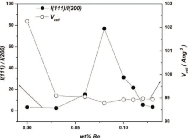
Figure 1 shows the X-ray diffraction (XRD) patterns of pure and Be-doped CdO ilms prepared on glass substrates. These patterns reveal that all the investigated ilms have a cubic Fm3m CdO structure. The undoped CdO ilm was polycrystalline of lattice parameter 0.4695 nm, as given in JCPDS9. It was found that Be-doping enhanced the [111] preferential orientation for the host CdO ilms that refers to improving the crystallinity. As a measure of relative preferential orientation (RPO), the intensity ratio (I(111)/I(200)) of pure and Be-doped CdO was considered. As shown on Figure 2, with increasing of Be doping level, RPO was increased getting a maximum value with 0.08%-Be ilm that became almost totally [111] oriented. Moreover, with increasing of Be doping level, the unit-cell volume of host CdO slightly decreased. This can be explained by smaller ionic size of Be2+ dopant comparing to Cd2+ ion.
There is no peaks corresponding to beryllium or its oxides found in the XRD patterns of Be-doped CdO. This implies that beryllium ions were dissolved into the lattice of CdO. Several possibilities for beryllium ions to be incorporated in the host CdO crystalline lattice structure; they could occupy structural interstitial positions, occupy empty locations of Cd ions, or replace for Cd ions. Doping by replacement of Cd2+ ions with Be2+ ions forming substitutional solid
solution (SSS) needs several conditions to be realised. The percentage difference of ionic radii of Cd2+ and Be4+ is
52.6%7 that is much larger than 15%, which is necessary
for the formation of SSS, according to the Hume-Rothery rules. Furthermore, beryllium oxide crystallises in hexagonal structure that is different from cubic CdO structure, which supports un-favourability for beryllium to form a SSS with
CdO. However, the close electronegativities (1.7 and 1.5 Pau for Cd and Be, respectively) support beryllium to be more favourable than Cd to interact with oxygen, which supports the formation of SSS. In general, the occupation of structural
Table 1. The measured resistivity (ρ), mobility (μel), carrier concentration (Nel), and bandgap (Eg) for pure and Be-incorporated
CdO ilms grown on glass substrate.
Sample ρ(×10
–4
Ω.cm) μel (cm 2/V.s) N
el(10
20 cm–3) Eg
(eV)
CdO 201 7.03 0.44 2.53
0.03% Be 14 74.5 0.6 2.44
0.06% Be 6.1 84.9 1.21 2.3
0.08% Be 5.48 93.2 1.23 2.41
0.10% Be 4.14 129.0 1.12 2.3
0.11% Be 6.5 79.6 1.21 2.15
0.12% Be 7.3 70.7 1.21 2.23
0.13% Be 11.2 63.8 0.87 1.74
Figure 1. X-ray diffraction patterns for pure and Be-doped CdO ilms
deposited on glass substrates. The radiation used was Cu Kα-line.
interstitial positions of CdO lattice by Be2+ (Be
i) ions is most
likely to happen. However, the interstitial incorporation of Be2+ ions disturbs the charge balance of the unit cell that
may be settled by creation of Cd2+ ion vacancies (V
Cd) and/or
formation of interstitial oxygen (Oi). These variations cause decrease in lattice parameter. Furthermore, some of the small-size Be2+ ions that occupy interstitial positions might
diffuse by thermal motion and occupy Cd2+-ion vacancies
(VCd) forming SSS-type of doping.
The mean X-ray crystallite size (CS) was estimated from the intensive (111) relection by using Scherrer equation10 to
be in the range 35-42 nm that is not sensitive to beryllium doping.
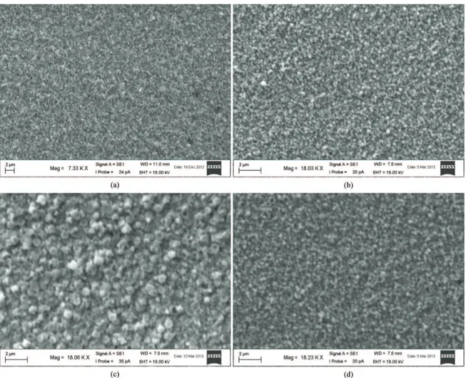
The SEM study demonstrates the morphological variations in CdO ilms because of beryllium doping. Figure 3 shows the SEM micrographs of un-doped CdO (Figure 3a), 0.06% Be-doped (Figure 3b), 0.10% Be-doped (Figure 3c), and 0.12% Be-doped (Figure 3d) CdO ilms. Thus, pure CdO ilm has woolly ibre shape microphotograph and with beryllium doping, the morphological structure was converted into a granular with almost round grains of size (GS) ~ 300 nm for 0.06% Be, ~600nm for 0.10% Be,
and ~200 nm for 0.12% Be. Thus, the GS increased with addition of beryllium attaining the utmost size in ~0.10% Be sample, referring to the highest crystallinity and therefore highest carrier mobility (next paragraph). Thus, the variation of GS with Be doping level is similar to that of RPO. It seems that Be doping with levels less than ~ 0.08-0.1% boosts the coalescence process between the grains.
3.2. DC-electrical properties
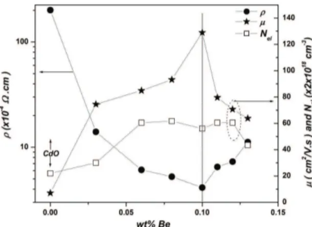
Table 1 and Figure 4 demonstrate the experimental results of electrical measurements on resistivity (ρ), mobility (μ), and carrier concentration (Nel) as a function of (Be/Cd)% wt ratio in different samples. The results reveal that, the n-conductivity and mobility are dependent on beryllium doping level so that with increasing of Be% they increased to utmost values before decreasing. The utmost mobility was ~130 cm2/Vs for ~0.10% Be ilms with a lowest resistivity
of 4.14×10⁻⁴ Ωcm. Figure 4 shows that with doping, the
carrier concentration increased rapidly by 175% in 0.06%Be ilm, then became almost constant (~ 1.2×1020 cm–3) before decreasing in 0.13% Be ilm.
According to the above results, three doping-level regions can be distinguished in Figure 4. In the lower dopant concentration region (Be%<0.06%), most of Be ions occupied CdO interstitials. They behave as donors in increasing the carrier concentration and at the same time they enhanced the carrier transportation, which leads to improve the carrier mobility and conductivity.
The middle doping-level region of Figure 4 is characterised by strong and continuous improving of mobility and conductivity with increasing of %Be content. In this region, the carrier transportation continued enhancement with increasing of %Be content. This occurs owing to the improvement in crystallinity by partial formation of SSS. This partial formation of SSS cannot increase the carrier concentration.
The third doping-level degradation region of Figure 4 (Be%>0.1%)can be described by a gradual accumulation of amorphous Be-oxide on crystallite (CB) and grain boundaries (GB). These accumulations form isolating potential barriers at CB and GB that led to decrease σ and
μ. Furthermore, because of high doping concentration, the crystallinity decreases and Be ions turn over to be hampers inhibit the motion of carriers that reduce the σ and μ.
Thus, in general, the variation behaviour of σ and μ with Be% doping level can be explained in conjunction with the structural variations induced by Be incorporation.
It is important to compare the present results with similar kind of doping process, i. e. doping of CdO with small-size ions. The mobility attained 85.2 cm2/V.s in 1.3% Cr-doped
CdO and 91 cm2/V.s in 0.25%Ge doped CdO5,6. This means
that doping with Be ions leads to better results for mobility, from TCO point of view.
3.3. Optoelectronic properties
The spectral transmittance T(λ) and relectance R(λ) of the prepared Be-doped CdO ilms grown on corning glass substrate in the region (300-3000 nm) are depicted in Figure 5a and Figure 5b, respectively. The better spectral transparent region (T >80%) of the ilms is being in the NIR spectral region
(λ > 900 nm). In addition, the high-wavelength sides of spectral transmittance, T(λ) for doped CdO samples show a clear damping, especially for higher doping level. The spectral relectance of the studied ilms depicted in Figure 5b show interference fringes that refer to their good quality; uniform and smooth. The spectral absorption coeficient α(λ) is related to the absorbance A(λ) by A (λ) = α (λ) d where d is the ilm’s thickness. The absorbance A (λ) that can be calculated byA(λ) = 1n [(1 - R) / T]11 is used to evaluate the direct optical band gap Eg by Tauc method12:
(
)
0.5op g
AE=B E−E (1)
where Bop is the ilm’s constant. The extrapolation of the linear portion of (ΑE)2 vs. E plot, as shown in Figure 6, gives
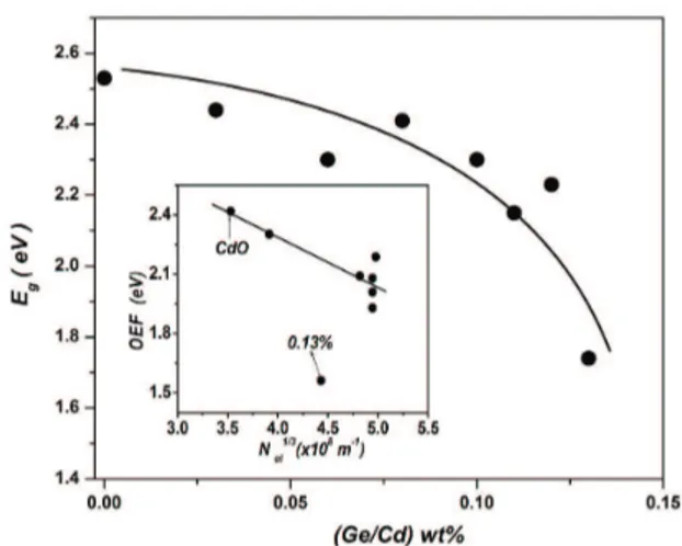
the direct bandgap (Table 1). The inset of Figure 6 gives Eg=2.53 eV for pure CdO ilm. The bandgap shrinks with
Figure 4. Variation of resistivity (ρ), carrier concentration (Nel)
and mobility (μ) with Be doping level of host CdO ilm grown on
glass substrates.
Be incorporation, as shown in Figure 7. Thus, bandgap may be engineered by Be% incorporation. The variation of bandgap with Be-doping has two components: the bandgap widening (BGW)13 and bandgap narrowing (BGN).14
Phenomenologically, the following relation correlates the bandgap(Eg) with the carrier concentration5,15:
(2)
2/3 1/3
g BGW,BGN e1 BGN e1 f
E =S N −S N +C (2)
where the coefficients 19 2
BGW,BGN
S =8.98x10− eVm and
9
BGN r
S =ε2.836x10− / , εr is the effective dielectric
constant of CdO at high wavelengths
(
2 2)
r n 1.6
ε = = ,
n is the refractive index, and Cf is a itting parameter. The optoelectronic function (OEF) is deined by:
2/3
g BGW,BGN el
OEF=(E −S N ) (3)
According to Equation 2, a straight line was obtained by
plotting optoelectronic function 1/3 e1
OEFvs.N , as shown in
the inset of Figure 7, which gives ( )2 9 BGN
S =2.3x10−eV.m
that is close to the theoretical value of 1.10×10⁻⁹ eV.m.5
The points corresponds to samples with higher Be content (> 0.11%) were not lie on the straight line because of partial accumulation of Be oxide on GB and CB creating potential barriers that reduce the effective conduction carrier concentration.
4. Conclusions
The structural study shows that the incorporated Be2+ ions
for up to 0.10 wt% doping level, were almost totally dissolved in the crystalline lattice of CdO. The dopant Be2+ ions mostly
occupying interstitial positions in CdO structure enhance the electronic conduction “highways” that improve the carrier mobility and conductivity. For more doping level (Be%>0.1%), Be ions turn over becoming hampers inhibit the motion of carriers that reduce the mobility and conductivity. The competition of these two opposite inluence doers controls the conduction parameters of Be-content CdO ilms. The utmost mobility was ~130 cm2/Vs for ~0.10% Be ilm with
a lowest resistivity of 4.14×10⁻⁴ Ωcm. This value of carrier
mobility is higher than that found with small ions like Cr-, W-, B-, and Ge-incorporated CdO ilms prepared by the same method and conditions, and thus is considered as one of the highest values found for doped CdO grown on glass substrate. The improvement of carrier mobility was observed in the present work accompanied with enlargement of grains and improvement in [111] crystalline orientation. From IR-TCO point of view, Be doping is suficiently effective for CdO light doping. The doping creates variations in structural and electronic energy spectrum that consequently leads to shrinkage the bandgap. The variation of bandgap with doping level was calculated in the framework of available models.
Acknowledgements
The author is grateful to Ms. H. Khalifa from Central Labs/College of Science/ SEM laboratory.
Figure 6. Tauc plots for Be-doped CdO ilms. The inset shows the
Tauc plot for undoped CdO.
Figure 7. Variation of bandgap (Eg) of host CdO ilms with Be doping level. The inset shows the N1/3el -dependence of the OEF =(E - Sg BGW , BGNNel2 / 3). The straight line shows the best
References
1. Calnan S and Tiwari AN. High mobility transparent conducting oxides for thin film solar cells. Thin Solid Films. 2010; 518(7):1839-1849. http://dx.doi.org/10.1016/j.tsf.2009.09.044.
2. Zhao Z, Morel DL and Ferekides CS. Electrical and optical
properties of tin-doped CdO films deposited by atmospheric metalorganic chemical vapor deposition. Thin Solid Films. 2002; 413(1-2):203-211. http://dx.doi.org/10.1016/S0040-6090(02)00344-9.
3. Burbano M, Scanlon DO and Watson GW. Sources of conductivity
and doping limits in CdO from hybrid density functional theory.
Journal of the American Chemical Society. 2011;
133(38):15065-15072. http://dx.doi.org/10.1021/ja204639y. PMid:21854046 4. Metz AW, Ireland JR, Zheng JG, Lobo RP, Yang Y, Ni J, et al.
Transparent conducting oxides: texture and microstructure effects
on charge carrier mobility in MOCVD-Derived CdO thin films
grown with a thermally stable, low-melting precursor. Journal of the American Chemical Society. 2004; 126(27):8477-8492.
http://dx.doi.org/10.1021/ja039232z. PMid:15238005
5. Dakhel AA and Hamad H. Investigation on high carrier mobility in chromium incorporated CdO thin films on glass. International
Journal of Thin Films Science and Technology. 2012; 1:25-33. 6. Dakhel AA. Germanium doping to improve carrier mobility
in CdO films. Advances in OptoElectronics. 2013; 2013:6 http://dx.doi.org/10.1155/2013/804646.
7. Shannon RD. Revised effective ionic radii and systematic studies of interatomic distances in halides and chalcogenides.
Acta Crystallographica. Section A, Crystal Physics, Diffraction, Theoretical and General Crystallography. 1976; 32(5):751-767. http://dx.doi.org/10.1107/S0567739476001551.
8. Chung JK, Kim WJ, Kim SS, Song TK and Kim CJ. Structural and optical properties of Be-doped ZnO nanocrystalline films by pulsed laser deposition. Thin Solid Films. 2008; 516(12):4190-4193. http://dx.doi.org/10.1016/j.tsf.2007.11.004.
9. Joint Committee for Powder Diffraction Studies – JCPDS. Powder diffraction file. File No. 05-0640.
10. Kaelble EF, editor. Handbook of X-rays for diffraction, emission, absorption, and microscopy. New York: McGraw-Hill; 1967.
11. Hong WQ. Extraction of extinction coefficient of weak absorbing thin films from special absorption. Journal of Physics. D, Applied Physics. 1989; 22(9):1384-1385. http:// dx.doi.org/10.1088/0022-3727/22/9/024.
12. Tauc J and Abelesn F, editors. Optical properties of solids. North Holland: North Holland Publ. Co.; 1969.
13. Pankove JI. Optical processes in semiconductor. Dover: Courier Corporation; 1975.
14. Zhang YZ, Lu JG, Ye ZZ, He HP, Zhu LP, Zhao BH, et al.
Effects of growth temperature on Li–N dual-doped p-type ZnO thin films prepared by pulsed laser deposition. Applied Surface Science. 2008; 254(7):1993-1996. http://dx.doi.org/10.1016/j. apsusc.2007.08.008.