Composite Screen-Printed Thick Films
for High Dielectric Constant Devices:
Bi
4
Ti
3
O
12
–CaCu
3
Ti
4
O
12
Films
K.D.A. Sabo´ia, P.B.A. Fechine, M.R.P. Santos, F.N.A. Freire, F.M.M. Pereira, A.S.B. Sombra
Laborato´rio de Telecomunicac¸o˜es e Cieˆncia e Engenharia dos Materiais (LOCEM), Departamento de Fı´sica, Universidade Federal do Ceara´, CEP 60455-760, Fortaleza, Ceara´, Brazil
In this paper, we did a study of the effect of the pres-ence of BIT (Bi4Ti3O12) in the dielectric and optical properties of the CaCu3Ti4O12 (CCTO) thick films. The films were prepared by the solid sate procedure. Me-chanical alloying followed by the solid state procedure has been used successfully to produce powders of CaCu3Ti4O12 (CCTO) and BIT (Bi4Ti3O12) to be used in the composites. We also look at the effect of the grain size of the BIT and CCTO in the final properties of the composite film. The samples were studied using X-Ray diffraction, scanning electron microscopy (SEM), Raman and infrared spectroscopy. We also did a study of the dielectric function (K) and dielectric loss (D) of the films. The role played by the grain size of CCTO and BIT in the dielectric constant and structural prop-erties of the films are discussed. These measurements confirm the potential use of such materials for small high dielectric planar devices. These films are also attractive for capacitor applications and certainly for microelectronics, microwave devices (mobile phones for example), where the miniaturization of the devices is crucial. POLYM. COMPOS., 28:771–777, 2007.ª2007 Soci-ety of Plastics Engineers
INTRODUCTION
Thin films of thickness below 1 mm have been
exten-sively investigated due to their potential applications in microelectronics and micromechanics. However, less atten-tion has been directed to processing of thicker films. A reasonable number of applications require films of several microns to several tens of microns. Ferroelectric thin films methods have their specific features, whereas ferro-electric thick films processing is closer to that of the bulk
ceramics, including powder synthesis, powder processing, coating, and sintering. Coating is obtained by screen printing, a well developed processing step in thick film technology.
Applications of ferroelectric thick films includes pyro-electric sensors [1, 2], gravimetric sensors [3], micropumps [4], pressure sensors [5], and surface acoustic wave sensors (SAW) [6] devices. Properties obtained are poorer compared to the bulk ceramics due to the addition of low temperature sintering aids and/or high porosity.
Most multichip modules (MCMs) fabricated today require decoupling capacitors to suppress the power distri-bution noise [7, 8]. These surface mount capacitors are large in size, occupy space, and have large parasitic capacitance. Materials with relative dielectric constant (K) in the range of 25–170 are required for advanced decou-pling capacitors.
High dielectric constants (K) have been found in oxides of the type CaCu3Ti4O12 [1–3] (CCTO), which shows a
dielectric constant (K) at 100 Hz of about 10,000 that is nearly constant from room temperature to 3008C. Oxides with the perovskite structure are well stabilized by their high dielectric constants (K), which lead these class of materials to a big number of technological applications [4]. However this behavior is generally associated to fer-roelectric or relaxor properties. In these cases, the highest value of K is obtained during a phase transition (as a function of temperature) presented by the material.
The existence of a transition temperature is generally a problem when one is talking about applications of these materials. The reported results for CCTO show that theK
is high with small dependence on the temperature [3]. Such material is very promising for capacitor applica-tions and certainly for microelectronics, microwave devi-ces (mobile phones for example), where the miniaturiza-tion of the devices are crucial.
HighK ceramics make it possible to noticeably minia-turize passive microwave devices. Their size can typically be reduced in comparison with classical resonators and filters by a factor of 1= ffiffiffiffi
K
p
(relative dielectric constant).
Correspondence to: A.S.B. Sombra; e-mail: sombra@fisica.ufc.br or WWW. LOCEM.UFC.BR
Contract grant sponsors: FINEP, CNPq, FUNCAP, and CAPES (Brazil-ian agencies).
DOI 10.1002/pc.20347
Published online in Wiley InterScience (www.interscience.wiley.com).
V
In this work, we will study a composite thick film with two different phases. The second ceramic will be the bismuth titanate Bi4Ti3O12-BIT. It belongs to the family
of ferroelectric materials with layered structures, which consists of three perovskite-like units (Bi2Ti3O102 ),
sand-wiched between bismuth oxide (Bi2O22þ) layers. BIT
single crystals has low dielectric constant and a very high Curie temperature (TC ¼ 6758C), which makes it useful
for various applications such as memory elements, optical displays, piezoelectric, and piroelectric devices in a wide temperature range from 20 to 6008C. Below room temper-ature, it shows a orthorhombic Fmmm symmetry, which exhibits ferroelectric properties [1, 2].
BIT ceramics have been used in capacitors, transducers, sensors, etc. [3, 4]. The tuning of specific electric proper-ties by compositional modification as well as the grain size effect could lead to modifications in the Curie tem-perature, conductivity, coercivity, compliance, etc. [5, 6].
Dielectric properties of BIT ceramics are highly de-pendent upon the grain size, phase content of the ceramic body, and sintering temperature. Dielectric constant (K) of BIT ceramics sintered around 8508C show values in the range of 235–250 in the frequency range of 100 Hz to 100 kHz. The dielectric loss (D) shows a little increase with values around 1.610 2in this frequency range [7].
Therefore, BIT-based ceramics can show a different dielectric behavior, depending on the particle size.
In this work, we report the preparation of the ceramic of CCTO and BIT through the solid state route and use these materials together to prepare composite thick films. The produced samples were studied using X-ray diffrac-tion, infrared and Raman spectroscopy, and scanning elec-tron microscopy techniques. The dielectric constant and the dielectric loss were also studied in the range of 100 Hz to 1 MHz. The production and the study of the properties of the BIT–CCTO films are important in view of possible applications, as in microwave and RF devices based in thick highKfilms.
EXPERIMENTAL METHODS
CCTO Crystalline Powder
Commercial oxides Ca(OH)2 (Vetec, 97% with 3% of
CaCO3), titanium oxide (TiO2) (Aldrich, 99%), CuO (Aldrich,
99%) were used in the CCTO preparation. The material was ground on a Fritsch Pulverisette 6 planetary mill with the proportionality of Ca(OH)2-3CuO-4TiO2. Milling was
performed in sealed stainless steel vials and balls under air. Mechanical alloying was performed for 30 min of milling. In this case, the milling was used only to give a good homogeneity of the powder. However, we already showed in the literature that for 100 h of milling the com-plete production of CCTO is possible [9].
The compounds were also prepared by the conven-tional powder-sintering technique using the same starting
materials. The ceramic was submitted to calcination and sintering (Table 1) in air in the range of 900 to 10208C for 12 h [10]. This ceramic is called CCTO100.
Paste Preparation
The paste was prepared from the suspension of organic material (resin, organic solvent, and some additive to improve rheological behavior of the paste) and powders of BIT and CCTO. To have a better adhesion between paste and substrate (Al2O3), a low temperature melting
material in powder form (flux material) was added.
Substrates and Electrodes
Alumina substrates were used as a commercial product (Engecer). The electrode material was produced for the screen printing technique (Joint Metal-PC200).
Preparation of the Films
The bottom electrodes (Ag) were screen printed on the Al2O3 substrate and fired at 8508C for 1 h. On the fired
electrode, a first layer was screen printed and sintered at for 1 h. After firing the dielectric layer, the upper elec-trode (Ag) was deposited, and after that, it was dried and fired at the same temperature–time regime as for the bot-tom electrode. The obtained films usually had thickness that ranged from 20 to 400mm, depending on the number
of layers. All the films used in these measurements were composed of two layers.
In this study, one has the films: CCTO100 (100% CCTO thick film), BIT X ((X)% of BIT and (100 X)% of CCTO) for X ¼ 10, 20, 50, 60, 80, and 100 thick film), where the percentage is given in weight percent.
The film was subjected to the firing process:
1008C for 1 hþ 4008C for 1 h þ 9008C for 1 h (first layer).
1008C for 1 hþ4008C for 1 hþ9008C for 4 h (second layer).
X-ray Diffraction
The X-ray diffraction (XRD) patterns were obtained at room temperature (300 K) by step scanning using
TABLE 1. Infrared modes of the samples BIT100 and CCTO 100.
Modes
Infrared modes (cm 1)
BIT100 BIT [12] CCTO100 CCTO [13]
n1(Ti O) s 476 476
n1(Ti O) 515 516
n1(Ti O) 561 561
n1(Ti O) s 588 580
powdered samples. We used 5 s for each step of counting time, with a Cu Ka tube at 40 kV and 25 mA using the
geometry of Bragg-Brentano.
Scanning Electron Microscopy
The photomicrographs of the films of CCTO and BIT were obtained on a Scanning Electron Microscope, Phillips XL-30, operating with bunches of primary elec-trons ranging from 12 to 20 keV, covered with a layer of carbon of 30 nm of thickness.
Dielectric Measurements
The dielectric measurements were obtained from a HP 4291A material impedance analyzer in conjunction with a HP 4194 impedance analyzer, which jointly cover the region of 100 Hz–1.8 GHz at room temperature (300 K).
Infrared Spectroscopy
The infrared spectra (IR) were measured using KBr pellets made from a mixture of powder for each glass composition. The pellet thickness varied from 0.5 to 0.6 mm. The IR spectra were measured from 400 to 1200 cm 1with a Nicolet 5ZPX FTIR spectrometer.
Raman Spectroscopy
Micro-Raman measurements were performed using a T64000 Jobin Yvon spectrometer equipped with an N2
-cooled charge coupled device (CCD) to detect the scat-tered light. The spectra were excited with an argon–ion laser (5145 A˚ ). The spectrometer slits were set to give a spectral resolution always better than 2 cm 1. The Raman
scattering was measured in a back scattering geometry directly from the powder.
RESULTS AND DISCUSSION
X-ray Diffraction
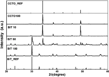
Figure 1 shows the X-ray diffraction (XRD) patterns of the samples BIT (X)–CCTO(1 X) together with the XRD of the references (JCPDS), associated to CCTO(CC-TO_REF) and BIT(BIT_REF), that were used in the sam-ple preparation (as discussed earlier). In the same figure, one starts with the XRD of sample BIT100. For this sam-ple, one can easily identify all the peaks associated to BIT phase. For the sample BIT80 (BIT80–CCTO20), the presence of the CCTO phase is very weak. Weak peaks around 34.88 and 49.38could be detected. For the sample BIT50 (BIT50–CCTO50), the presence of both phases is easily detected. The increase of the CCTO presence is quite clear. For the sample BIT10, the presence of BIT is quite weak. For the final sample in the series CCTO100, the CCTO presence is clear.
Infrared Spectroscopy
The infrared spectra of the samples in the series BIT(X)–CCTO(1 X) are shown in Fig. 2 and Table 1. The tetragonal BIT was characterized by the IR spectrum from octahedral TiO6 groups and the characteristic
adsorption bands appeared at 830, 580, and 390 cm 1 [11]. The bands above 405 cm 1 was due to the Ti O stretching vibration and the bands below 405 cm 1 are attributed to Ti O bending vibration [11]. Figure 2 shows the IR spectra of the BIT100 sample, where the modes at 816, 588, and 476 cm 1are identified. With the increase of the CCTO presence, the modes at 588 and 816 cm 1 associated to the BIT phase are very weak. From the
sam-FIG. 1. X-Ray diffraction of the samples in the series BIT–CCTO and reference samples (Joint Committee on Powder Diffraction Standards (JCPDS), International Center for Diffraction Data, 12 Camous Blvd., Newton Square, Pennsylvania 19073-3723, USA; 19995 – Pattern 93-1880 [BTO-REF], 75-1149 [CCTO-REF]).
ple BIT20, all the detected modes are associated to the CCTO phase. One can notice that the CCTO phase pres-ent resonance absorptions at 561 and 442 cm 1. Several authors have assigned [9, 13–15] this region of absorp-tions with the titanium ion. These bands were associated tonTi O¼653–550 cm
1
andnTi O Ti ¼495–436 cm 1
(Table 1).
In summary, one can say that the main bands associ-ated to BIT and CCTO were identified in the samples according with data from the literature.
Raman Spectroscopy
The Raman spectra of the samples of the complete se-ries BIT(X)–CCTO(1 X) are shown in Fig. 3 and Table 2. The Raman spectra of the CCTO sample (CCTO100) has three main peaks at 446, 512, and 576 cm 1 (Fig. 3), in good agreement with values reported in the literature [16– 18]. The Raman lines (Table 2) at 445 and 511 cm 1 have Ag symmetry (TiO6 rotation like). The peak at
576 cm 1 is associated to a mode of Fg symmetry
(O Ti O antistretching).
The Raman spectra of the BIT100 sample are shown in Fig. 3. Modes at 616, 572, 356, and 333 cm 1 could be assigned as the A1g and B1g modes, respectively
(Table 3); the 538,270, and 226 cm 1 modes could be assigned as B3g þB2g modes originating from the lifting
of Egdegeneracy.
The Raman modes of the samples BIT100 and CCTO100 are in good agreement with the values reported in literature [9, 11–13] (Table 2).
For the composite film BIT80, the presence of CCTO was very weak through the Raman spectra. For the BIT60 sample, the three modes associated to the CCTO phase are already present. For the BIT20 sample (Fig. 3), the
CCTO phase is dominant in the composite, and the BIT phase is not detectable.
Scanning Electron Microscopy
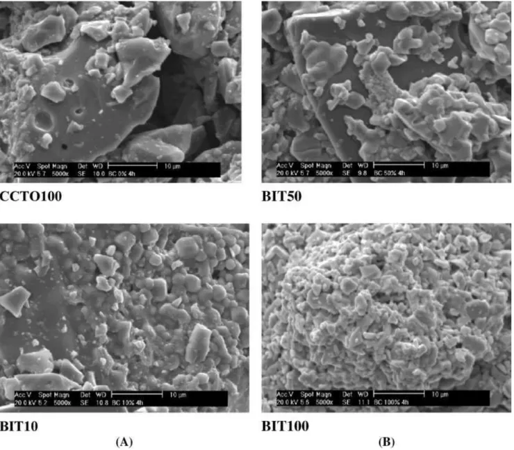
The particle morphology of the films was investigated by means of SEM. Figure 4A and 4B shows the scanning electron photomicrograph (5000) for samples CCTO100, BIT10, BIT50, and BIT100, respectively. In Fig. 4A, the
scanning electron photomicrograph for the CCTO100 sample is shown, where one can notice grains with dimen-sions around 10 mm or higher. The presence of shorter
grains is also detected. In Fig. 4B, the scanning electron photomicrograph for the BIT100 sample is shown. For the composite sample BIT50, both phases were present (Fig. 4B) and one can easily identify the grain size differ-ence between the phases. For the sample BIT10, a better interaction between the grains (where fusion between them is observed) is identified. The action of two grain sizes in the composite samples leads to important conse-quences in the electrical properties, which will be discussed later.
Dielectric Measurements
The dielectric constant measurements of all the sam-ples of the series BIT(X)–CCTO(1 X) are shown in Figs. 5 and 6. One can notice that for all the films the dielectric constant always decreases with the increasing in
FIG. 3. Raman spectra of the films in the BIT–CCTO series. Scanning electron photomicrograph of the BIT50–CCTO50 (5000).
TABLE 2. Raman modes of the samples BIT100 and CCTO 100.
Modes
Raman modes (cm 1)
BIT [12] BIT100 CCTO [13] CCTO100
B3gþB2g(O Ti O) 227 226
B3gþB2g(O Ti O) 268 270
A1g(O Ti O) 324 333
B1g(O Ti O) 346 356
Ag(TiO6) 445 446
Ag(TiO6) 511 512
B3gþB2g(O Ti O) 538 538
A1g(TiO6) 558 572
A1g(TiO6) 615 616
Fg(O Ti O) 575 576
TABLE 3. Dielectric permittivity (K) and dielectric loss (D) of the samples.
Sample Thickness (mm) K(100 Hz) D(100 Hz)
CCTO100 91 316.61 0.145 BIT10 149 409.71 0.168 BIT20 119 228.94 0.183 BIT50 96 122.85 0.103 BIT60 79 109.09 0.103 BIT80 142 67.99 0.064 BIT100 78 53.64 0.024
frequency (Fig. 5). For frequencies below 1 MHz, the K
value presented by the CCTO100 film is always higher than that presented by the BIT100 film. One can also notice that the BIT10 sample (BIT (10)–CCTO (90)) pres-ent the highest dielectric constant up to 1 MHz of fre-quency. At 100 Hz, the value of K is 316.61 for the CCTO100 sample and 53.64 for the BIT100 sample (Fig. 5). However, for the composite film, one has an unexpected result. The dielectric constant is higher for all the frequencies under study. At 100 Hz, the value of the
K is 409.71 for the BIT10 sample, which is around 20% higher when compared with the CCTO100 value for the same frequency (Table 3). Our previous observations of the difference in the grain sizes of the two phases (Fig. 4A and 4B) suggest that this difference in size for the composite leads to a more effective interaction be-tween grains, where little grains should more effectively
fill empty spaces in the composite. For the BIT10 sample, fusion between grains was observed (Fig. 4A). This could lead to more effective interface effects that could lead to a higher dielectric constant to a specific composite con-centration. This kind of effect was observed in other com-posites of the series of (BaTiO3) BTO–CCTO [16–19].
Figure 6 shows the dielectric loss for these films. At 100 Hz, the loss is lower for the BIT100 sample (2.4
10 2) and is higher for the BIT20 sample (18.3 10 2). The BIT100 sample presents the lowest loss for all the frequencies under study.
This amazing behavior observed for the composite sample, where one has higher Kvalue compared with that of the pure states, is probably associated with the sizes of the grains in both phases and to the interface between these grains. We are now looking the presence of this effect in the microwave region as well.
The classic treatment applied for two or more phases present in a dielectric are associated to the dielectric mix-ing rules that fix a limit to the dielectric constant that can be achieved with the mixed phase. The empirical logarith-mic rule for the dielectric constant K of the composite sample is given by [20]
logK¼X I
VIlogKI (1)
where (KI) is dielectric constant of the individual phases
and (VI) is the fractional volume of each phase. Figure 7
shows the plot of the dielectric constant (K) as a function of the film composition for several frequencies, based on
Eq. 1.
The continuous line is associated to the value of K
obtained fromEq. 1at 1 kHz.
The experimental points (for the frequencies 100 Hz, 1 kHz, 10 kHz, 100 kHz, and 1 MHz) of the samples are also indicated in the figure. One can easily conclude that the increase of the BIT phase in the BIT(X)–CCTO (100 X) composite is decreasing the K of the film at 1 KHz of frequency. However, forX ¼10%, the experi-mental value of the dielectric constant is higher when compared to the expected value suggested by Eq. 1 (K ¼
288) at 100 Hz. This is an unexpected behavior. It means that the composite is not following the linear regime of the model. This behavior is present in all the studied frequencies (below 1 MHz) (Fig. 7). In summary, seven different composite films of BIT–CCTO were studied in the medium frequency range (MF) of the spectra.
The dielectric permittivity K of all the films in the range of 100 Hz to 1 MHz was studied. For all the sam-ples, there is a decrease of theKvalue with frequency for this range of studied frequencies. The dielectric permittiv-ity K of the samples BIT (X)–CCTO (100 X) were studied in the range of 100 Hz to 1 MHz. One can observe that for the CCTO100 sample the dielectric constantK is higher when compared with that of the BIT100 sample for frequencies below 1 MHz. However, for the samples in which the BIT and CCTO form a composite ceramic, the dielectric constant is also decreasing with frequency.
One can say that the CCTO100 sample presents a higher value ofKat 100 Hz (316.61) when compared with the BIT100 sample (53.64). However, for the composite film BIT10 (BIT10–CCTO90) presents a surprising effect where the composite ceramic is not following the linear dielectric model with a K value 409.71 (Fig. 7), which seems to be a nonlinear mixing effect of the two phases.
CONCLUSIONS
In this paper, we did a study of the effect of the pres-ence of BIT (Bi4Ti3O12) in the dielectric and optical
pro-FIG. 6. Dielectric loss (D) as a function of frequency of the samples in the BIT–CCTO series.
FIG. 7. Dielectric permittivity for the medium frequency range. Contin-uous line obtained from Eq. 1(f ¼100 Hz, 1 kHz, 10 kHz, 100 kHz, and 1 MHz). Experimental points extracted from Fig. 5.
perties of the CaCu3Ti4O12 (CCTO) thick films. The
sam-ples were prepared by the solid sate procedure. Mechani-cal alloying followed by the solid state procedure has been used successfully to produce powders of CaCu3Ti4O12
(CCTO) and BIT (Bi4Ti3O12) to be used in the
compo-sites. The effect of the grain size of the BIT and CCTO in the final properties of the composite film was also stud-ied. The samples were studied using X-Ray diffraction, scanning electron microscopy (SEM), Raman and infrared spectroscopy. We also did a study of the dielectric func-tion (K) and dielectric loss (D) of the samples.
The X-ray diffraction (XRD) patterns of the samples BIT(X)–CCTO(1 X) concludes that the BIT and CCTO phases are present in the composite films.
The particle morphology of the films was investigated by SEM and suggests that the BIT sample shows a spheri-cal grain geometry with good densification. The CCTO sample presents a plate geometry for the grains with big-ger size, compared to the BIT sample. The action of two grain sizes in the composite samples is contributing to im-portant consequences in the electrical properties. The IR and Raman analysis shows the presence of the main Raman and IR modes associated to the BIT and CCTO phases reported in the literature [11–13, 19–21].
The dielectric constant (K) and loss (D) of the series BIT(X)–CCTO(1 X) was studied in the range of 100 Hz–1 MHz. One can notice that for all the samples the dielectric constant always decrease with the increase in frequency. For frequencies below 1 MHz, the K value presented by the CCTO100 sample is always higher than that presented by the BIT100 sample. At 100 Hz, the value of Kis 316.61 for the CCTO100 sample and 53.64 for the BIT100. However, for the composite samples, one has an unexpected result. The dielectric constant is higher for all the frequencies under study. At 100 Hz, the value of theK is around 409.71 for the BIT10 sample, which is around 20% higher when compared with the CCTO100 value for the same frequency, which seems to be a non-linear mixing effect of the two phases.
Our previous observations of the difference in the grain sizes of the two phases is suggesting that this difference in size for the composite is contributing to a more effec-tive densification of the sample, where little grains should more effectively fill empty spaces in the composite. This could lead to more effective interface effects that could lead to a higher dielectric constant to a specific composite concentration. The other point is that the BIT100 sample presents lower loss compared to all the other samples.
This amazing behavior observed for the composite sample is probably associated with the sizes of the grains in both phases and to the interface between these grains. We are now looking the presence of this effect in the microwave region as well.
Considering the classic treatment applied for two or more phases present in a dielectric and the empirical loga-rithmic rule for the dielectric constantKand the dielectric constants KI of the individual phases, one can conclude
that in the MF region of the spectra, the value of the dielectric constant is not in good agreement with the rule.
Looking now for highKand low loss film, which is the best option for use in microwave devices like dielectric res-onators, one has to find a balance between high dielectric constant and low loss. In a general view, the presence of the composite structure of BIT–CCTO leads to a strong increase of the dielectric constant of the composite. We expect to find an equilibrium situation with the maximum for the dielectric constant and lower loss in the composite.
This strongly suggests that the composites BIT–CCTO are good candidates for applications where one look for highKmaterials with low loss in radio-frequency range.
REFERENCES
1. B. Aurivilius,Ark. Kemi,1, 499 (1949).
2. J.F. Dorrain, R.E. Newnham, and D.K. Smith, Ferroelec-trics,3, 27 (1971).
3. T. Takenaka and K. Sakata,J. Appl. Phys.,55, 1092 (1984). 4. A. Fouskova and L.E. Cross,J. Appl. Phys.,41, 2834 (1970). 5. O.A. Fregoso,J. Appl. Phys.,81, 1378 (1997).
6. T. Takenaka and K. Sakata,Ferroelectrics,38, 769 (1981). 7. L.B. Kong, J. Ma, W. Zhu, and O.K. Tan,Mater. Lett.,51,
108 (2001).
8. M.A. Subramanian, D. Li, N. Duran, B.A. Reisner, and A.W. Sleight,J Solid State Chem.,323, 151 (2000). 9. A.F.L. Almeida, R.S. de Oliveira, J.C. Go´es, J.M. Sasaki,
J.M. Filho, and A.S.B. Sombra,Mater. Sci. Eng. B,96, 275 (2002).
10. M. Koch, N. Harris, R. Maas, A.G.R. Evans, N.M. White, and A. Brunnschweiler,Meas. Sci. Technol.,8, 49 (1997). 11. D. Chen and X. Jiao,Mater. Res. Bull.,36, 355 (2001). 12. W.L. Liua, H.R. Xia, H. Hand, and X.Q. Wang, J. Cryst.
Growth, in press.
13. S. Music, M. Gotic, M. Ivanda, S. Popovic, A. Turkovic, R. Trojko, A. Sekulic, and K. Furic,Mater. Sci. Eng. B,47, 33 (1997).
14. A.P. Ramirez, M.A. Subramanian, M. Gardel, G. Blumberg, D. Li, T. Vogt, and S.M. Shapiro, Solid State Commun.,
115, 217 (2000).
15. R.S. de Figueiredo, A. Messai, A.C. Hernandes, and A.S.B. Sombra,J. Mater. Sci. Lett.,17, 449 (1998).
16. V. Ferrari, D. Marioli, and A. Taroni, Meas. Sci. Technol.,
8, 42 (1997).
17. B. Morten, G. De-Cicco, and M. Prudenziati, Sens. Actua-tors A,31, 153 (1992).
18. W.G. Spitzer, R.C. Miller, D.A. Kleinman, and L.G. Howarth,Phys. Rev.,126, 5 (1962).
19. A.F.L. Almeida, P.B.A. Fechine, J.C. Go´es, M.A. Valente, M.A.R. Miranda, and A.S.B. Sombra, Mater. Sci. Eng. B,
111(2/3), 113A (2004).
20. M.I. Dı´az-Gu¨emes, T.G. Carrenˇo, and C.J. Serna, Spectro-chim. Acta A,45, 589 (1989).