Brazilian Journal of Physics, vol. 29, no. 4, December, 1999 623
Metal-Insulator Transition in Two Dimensions
S. V. Kravchenko
Physics Department, Northeastern University, Boston, Massachusetts 02115, U.S.A.
Received 27 May, 1999
A metal-insulator transition was recently observed in a variety of two-dimensional electron and hole systems, contrary to the 20 year old belief that it is forbidden in two dimensions. The origin of this transition is still unknown and is being debated. In this paper, I briey survey the main experimental ndings and suggested explanations.
Until recently, it was believed that all two-dimensional (2D) electron or hole systems are localized in the absence of a magnetic eld in the limit of zero temperature no matter how clean the 2D system is. This conclusion was based on scaling theory for non-interacting electrons [1] and even in the case of weakly interacting particles [2]. The theory [1, 2] received ex-perimental conrmation in a number of 2D materials (see, e.g., Ref.[3, 4]). However, measurements on very
clean 2D systems suggested that a transition from in-sulating to conducting behavior occurs with increasing
electron (hole) density, ns, above some critical density,
nc [5-12]. It was quickly realized that this transition
occurs in the regime of high rsvalues where
rs
Eee
EF
= me2
4(ns) 1=2
~ 2
0
(1) is the ratio of the energy of electron-electron interac-tions and the Fermi energy (here m is the eective
mass and is the dielectric constant). In most 2D systems where this unexpected transition was found, rs values were of the order of 10. Therefore, rather
than being a small perturbation, correlations provide the main energy in the problem. Strongly interacting 2D systems are currently the focus of intense theoretical interest [13-20].
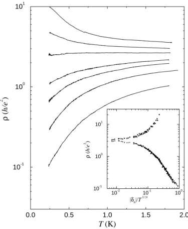
A typical temperature dependence of the resistiv-ity of a high-qualresistiv-ity 2D system (silicon metal-oxide-semiconductor eld-eect transistor, \MOSFET") in a \dilute" (high rs) regime is shown in Fig. 1 on a
semi-logarithmic scale. Dierent curves correspond to dif-ferent electron densities which are set by the voltage applied between the gate and the 2D layer. The
re-sistivity increases with decreasing temperature for the two lower electron densities indicating insulating (\nor-mal") behavior. For the four highest ns, the resistivity
sharply decreases with decreasing temperature
signal-ing a transition from insulatsignal-ing to conducting
behav-ior. At a critical density nc = 9:02 10
10cm,1 the
resistivity is practically temperature-independent. This temperature-independent point corresponds to the crit-ical electron density for the metal-insulator transition. Qualitatively the same (T) dependencies were re-cently obtained in other 2D systems: p-SiGe het-erostructures [7], p-GaAs/AlGaAs hethet-erostructures [8, 9], n-AlAs heterostructure [10], and n-GaAs/AlGaAs heterostructure [11]. A common feature of all these 2D systems is that the transition from insulating to appar-ent metallic behavior is seen at relatively high values of rs. Another common feature is that the \critical" value
of the resistivity at the transition, c (n
c), is of the
order of the quantum of resistivity, h=e2.
An important feature of the (T) dependencies around the metal-insulator transition is the fact that they can be \scaled" onto two distinct branches. In other words, the family of (ns;T) curves can be
rep-resented as a function of =Tb where (n
s ,n
c)=nc
624 S.V.Kravchenko
10-2 10-1 100
|δn|/T 1/zν
10-1 100 101
ρ
(
h
/e
2 )
0.0 0.5 1.0 1.5 2.0
T (K)
10-1
100
101
ρ
(
h/e
2 )
Figure 1. Resistivity of Si MOSFET in zero magnetic eld as a function of temperature for electron densities
ns= 8.58, 8.80, 9.02, 9.33, 9.52, 9.90, and 1.1010
10cm,2.
The critical density for the metal-insulator transition is 9:0210
10 cm,2. The inset demonstrates scaling of the
resistivity with temperature (after Ref. [5]).
One of the most interesting characteristics of the anomalous conducting phase is its dramatic response to a magnetic eld applied parallel to the plane of the 2D system. An example of this behavior is shown in Fig. 2. The resistivity of silicon MOSFET increases by more than two orders of magnitude with increasing eld, saturating to a new value in elds above2 Tesla
[21, 22]. Apparently, the magnetic eld drives a con-ducting system into an insulating state. However, in contrast with the n
s-driven metal-insulator transition,
there appear to be no \critical" value of magnetic eld below which the system remains conducting and above which it becomes insulating. In Ref.[21], a conclusion was made that a conducting state is suppressed by an arbitrary weak magnetic eld. However, more recent measurements on a high-quality p-GaAs/AlGaAs sug-gest that such a critical magnetic eld does exist [23]. This is currently an open question. We note that a parallel magnetic eld couples only to the spins of the electrons and not to their orbital motion. Therefore,
spins are believed to play a crucial role in the conduct-ing phase.
0 2 4 6 8
B|| (Tesla)
10-2
10-1
100
101
102
103
ρ
(e
2 /h
)
δ = 0.098
δ = 0.341
Figure 2. Resistivity of Si MOSFET as a function of par-allel magnetic eld on the metallic side of the transition at
T = 0:25 K. Upper curve: (n s
,n
c) =n
c= 0
:098; lower
curve: = 0:341.
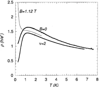
Very recently, an interesting similarity in(T)
be-tween zero magnetic eld case and an integer quantum Hall eect (QHE) state was observed in Si MOSFET [24]. As shown in Fig. 3, at both B = 0 and at the
Landau level lling factor = 2, (T) grows as the
temperature is decreased, reaches a maximum around
T
M
1 K, and rapidly drops at lower temperatures. In
contrast, the temperature dependence is very dierent at intermediate values of magnetic eld, as shown by the dotted curve of Fig. 2 (a). In principle, the simi-larity between (T) at B = 0 and = 2 may be
acci-dental and simply due to the fact that the resistance in both cases decreases from a \classical" value aboveT
M
to a low-temperature \quantum" value. On the other hand, there may be a deeper connection between the
B = 0 and QHE states. A similaritybetween the
metal-insulator transition in B = 0 and the QHE-insulator
transition was reported recently by Hanein et al.[25].
Brazilian Journal of Physics, vol. 29, no. 4, December, 1999 625 evolves smoothly and continuously to the B = 0
tran-sition discussed above. The critical resistivity at the QHE-insulator and B = 0 metal-insulator transition
were found to be surprisingly close to each other. These ndings raise the possibility that the B = 0
metal-insulator transition and QHE-metal-insulator transition are physically related.
Figure 3. Temperature dependencies of the diagonal resis-tivity of Si MOSFET atB = 0 and at Landau level lling
factor = 2 for ns = 0:7410
11 cm,2. The dotted line
shows the resistivity atB= 1:12 Tesla.
Many theoretical explanations for the unanticipated
B = 0 metal-insulator transition were suggested
re-cently [13-20]. Some of them [13, 14] are based on the pioneering work done by Finkelshtein in the early 1980's where a metallic state was predicted in strongly inter-acting 2D systems. This state would be suppressed by a magnetic eld in agreement with the experiment. How-ever, the mechanism suggested in Ref.[13] predicts an onset for the metallic phase at temperatures that are lower than those found experimentally: in most sys-tems, the drop in resistance is already seen at tem-peratures
1
3 E
F =k
B, while in Ref. [13], the condition T << ~=k
B
<< E
F =k
B was assumed (here E
F is
the Fermi energy and is the scattering time of the
electron). This discrepancy was addressed in Ref.[14] where it was shown that the metal-insulator transition should be evident at temperatures of the order of the Fermi temperature. Other suggested models are based on non-Fermi liquid state [16, 17]. Transition to an in-sulating behavior atn
s <n
c is attributed in Ref.[17] to
a formation of a Wigner solid. This prediction recently received a strong experimental support [12]. A possi-bility of having a \more traditional" non-Fermi liquid
in 2D semiconductor-based systems | superconducting state | was also considered [18]. Recent ndings of a critical magnetic eld seem to support this possibility. Other possible explanations are based on strong spin-orbit interaction [19]. There are also a few papers [20] in which the metal-insulator transition and other unusual properties of dilute 2D systems were attributed to clas-sical eects such as temperature-dependent screening and charging/discharging of the ions which are known to exist close to the interface. The fact that despite all eorts, there is still no consensus in the theory sug-gests that there may be unusual new physics behind the
B= 0 metal-insulator transition in 2D.
Experimental results shown in Figures 1-3 were obtained in collaboration with D. Simonian, M. P. Sarachik, K. Mertes, V. M. Pudalov, and T. M. Klapwijk. This work was supported by the National Science Foundation under Grant No. DMR-9803440.
References
[1] E. Abrahams, P. W. Anderson, D. C. Licciardello, and T. V. Ramakrishnan, Phys. Rev. Lett.42, 673 (1979).
[2] B. L. Altshuler, A. G. Aronov, and P. A. Lee, Phys. Rev. Lett.44, 1288 (1980).
[3] D. J. Bishop, D. C. Tsui, and R. C. Dynes, Phys. Rev. Lett.44, 1153 (1980).
[4] M. J. Uren, R. A. Davies, M. Kaveh, and M. Pepper, J. Phys. C44, 5737 (1981).
[5] S. V. Kravchenkoetal., Phys. Rev. B50, 8039 (1994);
Phys. Rev. B 51, 7038 (1995); Phys. Rev. Lett. 77,
4938 (1996).
[6] D. Popovic, A. B. Fowler, and S. Washburn, Phys. Rev. Lett.79, 1543 (1997).
[7] P. M. Coleridge, R. L. Williams, Y. Feng, and P. Za-wadzki, Phys. Rev. B56, R12764 (1997).
[8] Y. Haneinetal., Phys. Rev. Lett.80, 1288 (1998).
[9] M. Y. Simmonsetal., Phys. Rev. Lett.80, 1292 (1998).
[10] S. J. Papadakis and M. Shayegan, Phys. Rev. B 57,
R15068 (1998).
[11] Y. Haneinetal., Phys. Rev. B58, R13338 (1998).
[12] J. Yoon, C. C. Li, D. Shahar, D. C. Tsui, and M. Shayegan, preprint cond-mat/9807235 (Phys. Rev. Lett., in press).
[13] A. M. Finkelshtein, Z. Phys. B 56, 189 (1984); C.
Castellani, C. Di Castro, P. A. Lee, and M. Ma, Phys. Rev. B30, 527 (1984); C. Castellani, C. D. Castro, and
P. A. Lee, Phys. Rev. B57, R9381 (1998)
[14] Q. Si and C. M. Varma, Phys. Rev. Lett. 81, 4951
[15] V. Dobrosavljevic, E. Abrahams, E. Miranda, and S. Chakravarty, Phys. Rev. Lett.79, 455 (1997).
[16] S. Chakravarty, L. Yin, and E. Abrahams, Phys. Rev. B58, R559 (1998).
[17] S. Chakravarty, S. Kivelson, C. Nayak, and K. Voelker, preprint cond-mat/9805383 (1998), submitted to Na-ture(1998) (unpublished).
[18] P. Phillips et al., Nature 395, 253 (1998); D. Belitz
and T. R. Kirkpatrick, Phys. Rev. B58, 8214 (1998);
J. S. Thakur and D. Neilson, Phys. Rev. B58, 13 717
(1998).
[19] Y. Lyanda-Geller, Phys. Rev. Lett.80, 4273.
[20] S. He and X. C. Xie, Phys. Rev. Lett.80, 3324 (1998);
B. L. Altshuler and D. L. Maslov, Phys. Rev. Lett.82,
145 (1999); T. M. Klapwijk and S. Das Sarma, preprint
cond-mat/9810349 (1998) (Solid State Commun., in press); S. Das Sarma and E. H. Hwang, preprint cond-mat/9812216 (1998) (unpublished).
[21] D. Simonian, S. V. Kravchenko, M. P. Sarachik, and V. M. Pudalov, Phys. Rev. Lett.79, 2304 (1997).
[22] V. M. Pudalov, G. Brunthaler, A. Prinz, and G. Bauer, JETP Lett.65, 932 (1997).
[23] J. Yoonetal., abstract LC30.06 (1999 March Meeting
of the APS).
[24] S. V. Kravchenko et al., preprint cond-mat/9812389
(1998) (submitted to Phys. Rev. B).
[25] Y. Hanein et al., preprint cond-mat/9901186 (1999)