Brazilian Microwave and Optoelectronics Society-SBMO received 14 May 2018; for review 14 May 2018; accepted 20 Jun 2018 Abstract— In this paper an electrical model for square bifilar
planar spiral coils (BPSC) is presented. Its main aim is the study of BPSC electrical parameters and behavior involving the frequency range where the first resonances (valley and peak) occur for bifilar coils in open-circuit configuration. A new approach to determine mutual capacitances of BPSCs based on coplanar waveguide (CPW) lines is presented. This study can be applied for modeling of passive self-resonant (PSR) sensors and wireless power transfer (WPT) systems. In order to validate the proposed model, three BPSCs were manufactured, tested by means of an impedance analyzer and also submitted to electromagnetic (EM) simulations. The results obtained, presented by means of tables and graphs, show that the present study is feasible and promising for the modeling of open square BPSCs.
Index Terms— Bifilar Coil, Electrical Modeling, Planar Spiral Coil, Self-Resonance.
I. INTRODUCTION
The conception of bifilar winding dates back to the last decade of the nineteenth century and is related to studies of the Serbian engineer Nikola Tesla (1856-1943) in the development of electrical devices intended to transmit and distribute high frequency electrical energy [1]-[2].
(a) (b) Fig. 1. Helical monofilar (a) and bifilar (b) coils.
As an example, Fig. 1 shows the difference between the winding method of a monofilar and bifilar coil for the helical shape. According to [3], considering both coils of the same shape, diameter, wire spacing and same turn number, the mutual capacitance arising between bifilar coil windings is significantly greater than the self-capacitance [4] arising in the terminals of the monofilar coil. This is due to fact that the average voltage between adjacent turns in the bifilar coil is greater than in the monofilar coil by a proportionality ratio that is function of the number of turns [3], [5]. Thus, the higher the number of turns, the higher the rate of proportionality between these two capacitances. Consequently, this makes the first self-resonance frequency of the bifilar coil significantly smaller
Modeling of Open Square
Bifilar Planar Spiral Coils
Denivaldo P. da Silva1 and Sérgio F. Pichorim2
Graduate School of Electrical Engineering and Applied Computer Sciences (CPGEI) Federal University of Technology - Paraná (UTFPR), Curitiba-PR, Brazil
than the one of a monofilar coil. This is an advantage, for example, in biomedical applications where the signal received by a reader coil from an implanted sensor in a biological tissue tends to be less attenuated with frequency reduction [6].
In addition to the helical shape [3], [5], [7] the bifilar coil also may have Archimedean planar spiral [8], square planar spiral [9], [10], hexagonal planar spiral or even octagonal planar spiral shapes [11]. However, thispaper is limited only to the study of the square bifilar planar spiral coil (BPSC).
When manufactured on printed circuit board (PCB), square BPSCs may present lower manufacturing complexity than hexagonal, octagonal and, in particular, Archimedean BPSCs because their tracks maintain angles of 90 degrees between them [12].
BPSC can be applied, for example, as a passive self-resonant (PSR) sensor in the monitoring of soil [9] and wood [10] moisture, as well as for monitoring pressure, force and displacement [11]. This monitoring is done, indirectly, by successive measurements of parallel resonance frequencies, where the first impedance peak occurs. These variations in the resonance frequency are due to the variations suffered by the physical quantity monitored.
PSR sensor resonates at a certain self-resonant frequency without the aid of external capacitors due to the inductive and capacitive effect that occurs in their metal tracks and the influence of the medium that surrounds them. Generally, they are small, in the order of a few tens of millimeters, manufactured in PCB and coated with solder mask to protect against corrosion and short circuits between copper tracks.
At low frequencies and disregarding resistive losses, the bifilar coil can be modeled, in the open-circuit and closed-open-circuit configurations, as being two monofilar coils B1 and B2 with terminal pairs (1)-(2) and (3)-(4) and with their self-inductances Ls1 and Ls2 that are magnetically coupled with a mutual inductance M, as shows Fig.2.
(a) (b)
Fig. 2. Simplified lossless electrical models of a bifilar coil in the open-circuit configuration (a) and in the closed-circuit configuration (b).
In its 1894 patent, Tesla has studied only the closed-circuit configuration of its bifilar coil as in Fig. 2(b), but this coil can also be studied in the open-circuit configuration without the jumper between terminals (2)-(3), as shown in Fig. 2(a). However, regardless of the studied configuration (open or closed) the bifilar coil is generally analyzed by its terminals (1)-(4).
B2 B1
(1)
(2)
B2 (3)
(4) B1
(1)
(2)
(3)
(4)
Brazilian Microwave and Optoelectronics Society-SBMO received 14 May 2018; for review 14 May 2018; accepted 20 Jun 2018
The current studies on square BPSC are generally still restricted to closed-circuit configuration for application as PSR sensor as in [9], [10]. However, in open-circuit configuration, two BPSCs can be applied also for wireless power transfer (WPT) through their series resonances where the first impedance valley occurs, just as in [7] where tests with helical coils were performed.
Impedance curve of the open BPSC can be obtained by an impedance analyzer, but for the design of BPSC, it is interesting to predict it by means of an electric model that can determine with accuracy the first valley and the first peak of resonance.
Studies on modeling of open BPSCs acting at the series and parallel resonances are still rare. In [11] an open square BPSC is shown, but an electric model is not provided. In [8] the open BPSC is presented in the Archimedean shape, but the authors adopted an ideal electric model that covers only one resonance frequency and with an error of 22% relative to measured data.
This paper presents an electric model for the open square BPSC thatcovers the first valley and the first peak of resonance. The electrical parameters of this model were obtained and a new approach to determine mutual capacitances of BPSCs, based on coplanar waveguide (CPW) lines, is presented. In order to validate the proposed model, three square BPSCs were manufactured in double-sided PCB with FR-4 substrate and coated with solder mask. These BPSCs were tested by an impedance analyzer and also submitted to electromagnetic (EM) simulations. Tables and graphics were produced aiming to establish a comparative analysis between the results obtained with the proposed model, by EM simulation, as well as for the measured values.
II. MODELING OF OPEN SQUARE BPSC
Fig. 3 shows, as an example, an open square BPSC with N=4 turns, formed by two monofilar planar spiral coils (PSC), each one with Nm=2 turns, where w is the width of the copper track and s is the spacing between these tracks and each turn being formed by four consecutive straight segments.
In practice, the manufactured BPSC still requires underpass tracks with the function of interconnecting the center of this planar coil to external terminals in order to connect it to an impedance analyzer for testing. Although BPSC generally has only one underpass track for each monofilar winding, the BPSC of Fig. 3 was designed with two underpass tracks for each monofilar winding in order to facilitate measurements between its terminals. The width wov of the underpass
Fig. 3. Open square BPSC with N=4 turns, external side Doutb, internal side Dinb, formed by the monofilar PSC B1 with
terminals (1)-(2) and by monofilar PSC B2 with terminals (3)-(4), each one with Nm=2 turns, track width w, external side
Doutm, internal side Dinm, spacing s between tracks and with two underpass tracks of width wov.
Fig. 4. Electrical model proposed for an open square BPSC.
In Fig. 4, an electrical model of an open square BPSC of symmetrical layout is proposed. All parameters of resistances, inductances and capacitances (R, L, and C) distributed in B1 and B2 monofilar windings are considered identical, being
Rs series resistance of the tracks of each monofilar winding (B1 and B2),
Cp total stray capacitance that arises between the turns of each monofilar winding,
Rp resistance related to losses in dielectric materials and in the medium surrounding BPSC's tracks
Dinm
(2) (2)
(3)
(4) (1)
Doutm
Doutb
s
w
Doutb
Doutm
Dinb
w (4) underpass track wov
1
2
3
4
Brazilian Microwave and Optoelectronics Society-SBMO received 14 May 2018; for review 14 May 2018; accepted 20 Jun 2018
and that arises between turns of each monofilar winding,
Cm mutual capacitance that arises between B1 and B2 monofilar windings and
Rm resistance related to losses in dielectric materials and in the medium surrounding BPSC's tracks
and that arises between B1 and B2 monofilar windings.
Resistance Rm and capacitance Cm are distributed in the electrical model of Fig. 4 into two parts and
are referred as Rmm and Cmm, being
and
(1)
(2)
Although resistances Rs, Rmm and Rp have a fundamental role in the impedance frequency response
curve of the proposed model, in order to estimate the first valley ω1v (or f1v) and the first resonance peak ω1p (or f1p) for the open square BPSC, the model described in Fig. 4 will be simplified by excluding the resistive losses, since their effect on resonant frequencies can be considered negligible. This simplification will result in the impedance seen by terminals 1-4 as
(3)
being the angular frequency and the respective resonant frequencies are
and
(4)
(5)
As an example, Fig. 5 shows the Z14 impedance modulus and phase curves obtained by electromagnetic simulations and measurements made by an impedance analyzer, for an open square BPSC with N=28, manufactured in double-sided PCB, with FR-4 substrate, coated with solder mask,
w= 0.55 mm, wov=0.25 mm, s=0.45 mm, Doutb=65.55 mm and Dinb=10.45 mm. As will be shown in
Fig. 5. Module and phase curves of Z14 versus frequency f to simulated and measured data of an open square BPSC with
N=28 and localization of the first valley (f1v) and of the first resonance peak(f1p).
A. Inductances and Magnetic Coupling Factor
For an open square BPSC of symmetrical layout which inductances of the B1 and B2 monofilar windings are considered identical, self-inductance Ls can be determined by equation
as presented in [13] for square PSCs and the mutual inductance M by the equation
(6)
being
(7)
(8)
, (9)
, (10)
, (11)
and (12) , (13) where is the air magnetic permeability, is the BPSC’s average side, Lb is its
total inductance between terminals 1-4 with terminals 2-3 interconnected, is the fill ratio of each monofilar PSC and is the BPSC’s fill ratio.
BPSC is analyzed in the closed-circuit configuration only for the calculation of total inductance Lb.
All other inductances and capacitances of the proposed model will be determined with the BPSC in open-circuit configuration.
f1v
f1p
Resonance Valley
Brazilian Microwave and Optoelectronics Society-SBMO received 14 May 2018; for review 14 May 2018; accepted 20 Jun 2018
Again, considering the self-inductances of the monofilar windings B1 and B2 as being identical and using equations (6) and (7), the magnetic coupling factor is determined by the equation
(14)
The inductance calculation presented in [13] is based on approximating the sides of each monofilar PSC as current sheets, being its maximum error limited to 8% for PSCs with s/w < 3.
B. Capacitances
Mutual capacitance Cm is a capacitance that arises between pairs of tracks belonging to B1 and B2
monofilar PSCs which are mutually coupled.
This capacitance will be determined considering that the BPSC can be formed by CPW lines with finite-width lateral ground plane, assuming such ground plane width equal to w [14]-[15].
It considers, initially, an alternating signal source applied to terminals 1-3 of Fig. 3 with potential
V1 being instantaneously greater than V3. For the calculation of capacitance Cm only the contributions
of pairs of capacitances Ct that form between adjacent parallel tracks and that can represent a
three-wire line (CPW) are taken into account. From this premise, capacitance pairs Ct are distributed along
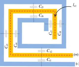
almost all tracks, with the exception of the first two outermost tracks and the last two innermost ones of the monofilar PSC B1, according to Fig. 6. Thus, the average length lav used for the calculation of
Cm is
– – . (15)
Fig. 6. Distributed capacitances Ct along of three-wire parallel tracks that totalize an average length lav. These three-wire
parallel tracks form four CPW lines, obtained from the BPSC with N=4 of Fig. 3, discounting the first two outermost tracks and the last two innermost ones of monofilar PSC B1.
Fig. 7 shows the cross-section of only three adjacent parallel tracks of a BPSC which represent a CPW line with finite-width lateral ground plane surrounded by three dielectric materials: the top and bottom layers contain a solder mask with dielectric constant, respectively, εr1 and εr3 and between
Ct8
Ct5
Ct3
Ct1 Ct6
Ct7
Ct4
C t2
lav
these two layers there is an FR-4 substrate with dielectric constant εr2. It should also be considered that these dielectric materials have relative heights and and that the medium surrounding the BPSC is the air.
Fig. 7. Cross section of a CPW for modeling of mutual capacitance Cm of a BPSC.
Applying the conformal mapping and superposition of partial capacitances techniques to the scheme shown in Fig. 7, the capacitance per unit length of a CPW can be expressed as [15]
, (16)
where is the effective relative permittivity and is the partial capacitance of the CPW in free space (vacuum or air). (17)
where εo is the electric permittivity of the vacuum (8.8542.10 -12 F/m) and K(ko) and K(k'o) are the complete elliptic integrals of the first kind that can be calculated by equations (18)
(19)
(20)
(21)
(22)
and (23) (24)
The effective relative permittivity is determined by equation (25)
w s
w
c
εr2
εr1
εr3
Brazilian Microwave and Optoelectronics Society-SBMO received 14 May 2018; for review 14 May 2018; accepted 20 Jun 2018
being
(26)
(27)
(28)
(29)
and
(30)
where is the filling factor, and are elliptic integral moduli and is the relative height of the dielectric layer i, being i varying from 1 to 3 is the indice associated to each one of the three dielectric layers shown in Fig. 7.
Thus, multiplying the equation (16) by (15), the mutual capacitance of the BPSC can be determined from the equation
(31)
The calculation of the mutual capacitance of BPSCs using CPW lines approach, proposed in this paper, will be compared with measured values only in section III. However, in order to test the validity of equation (31), comparisons were made with results obtained by EM simulations and with the calculation of mutual capacitances modeled by coplanar striplines (CPS) used in [8].
For this purpose, EM simulations were performed with three groups of 10 BPCSs, according to Tables I to III, in order to determine the mutual capacitance values CmEM. For each group of 10
BPSCs, w, s, Dinb and the parameters of Table IV were kept fixed, the only variables being Nm and
Doutb, according to Tables I to III. The fixed parameters described in Table IV, common to all three
groups of BPSCs are associated with Fig. 7, being the metal track thickness of the BPSC and (i =1 to 3) the loss tangent of each dielectric layer of the BPSC.
TABLE I. GROUP1- BPSCs TABLE II. GROUP 2 - BPSCs TABLE III. GROUP 3 - BPSCs
Nm 5 to 14 Nm 5 to 14 Nm 5 to 14
w 0.80 mm w 0.55 mm w 0.55 mm
s 0.20 mm s 0.45 mm s 0.20 mm
Doutb 29.80 mm to 65.8 mm Doutb 29.55 mm to 65.55 mm Doutb 34.30 mm to 61.30 mm
TABLEIV.ALLGROUPS-FIXEDPARAMETERS
39 µm (metal track thickness)
50 µm (top solder mask) 1.58 mm (FR-4 substrate)
1.62 mm (bottom solder mask of 40 µm )
4.00 4.85 4.00
0.035
0.018
0.035
(a) (b)
(c)
Fig. 8. Plots of mutual capacitance versus Nm for BPSCs (a) from group 1, (b) from group 2 and (c) from group 3: for Cm
using the CPW lines approach proposed in this paper, for CmEM using EM simulations and by CPS lines used in [8].
proposed approach ref. [8]
EM simulations
proposed approach ref. [8]
EM simulations
proposed approach ref. [8]
Brazilian Microwave and Optoelectronics Society-SBMO received 14 May 2018; for review 14 May 2018; accepted 20 Jun 2018
Next, the values of Cm obtained by CPW lines approach and those obtained by EM simulation, for
the three groups of BPSCs described in Tables I to III, were compared with the respective mutual capacitances modeled by CPS lines used in [8]. Results are presented in Fig. 8.
As shown in Fig. 8, the modeling of mutual capacitances using CPW lines proposed in this paper results in values of Cm that are very close to the results obtained by EM simulations. For BPSCs of
groups 1 to 3, the error of Cm relative to CmEM ranged from 1.69% to 12.92%, whereas the error using
the CPS lines approach proposed by [8] ranged from 30.20% to 46.93%.
According to equation (4), Cm is related only with the first resonance valley of the open BPSC,
whereas the total stray capacitance Cp is associated with the first valley and with the first resonance
peak, as presented in equation (5), and is defined as
(32)
where Cs is the stray capacitance, named also as self-capacitance [4], that arises between the turns of
each monofilar spiral winding present in the BPSC’s top layer, and Cov is the stray capacitance that
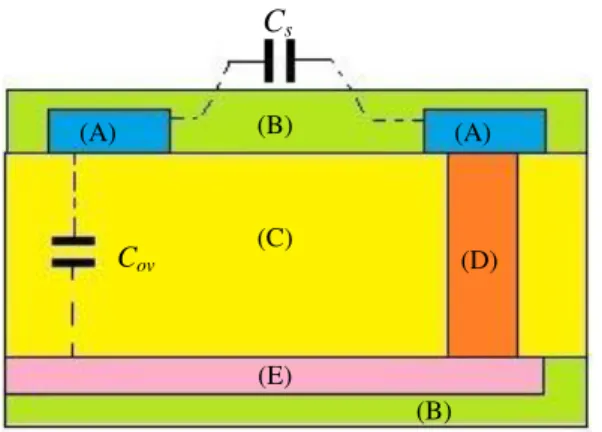
arises between the top layer tracks and the underpass tracks, according to Fig.9.
Fig. 9. Cross section of a BPSC showing where the capacitances and arise in the monofilar PSC B2: (A) are tracks of the PSC B2, (B) solder mask layers, (C) substrate layer and (D) a via which interconnects the center of the flat coil to the
underpass track (E). For simplicity, in this figure one single underpass track was represented.
While mutual capacitance Cm was calculated using a distance s between adjacent tracks, the
self-capacitance Cs is associated with a distance 2s between adjacent tracks and not 2s + w.As shown in
Fig. 6, between two spacing s there is a conductive track of width w that does not contribute to the calculation of self-capacitance, because the electric field inside the conductor is null. Thus, as a first estimate, the self-capacitance of monofilar PSC could, in principle, be calculated as
(33)
However, this first approximation for self-capacitance is not yet consistent with results obtained by EM simulation, because for the calculation of Cm it was assumed a constant potential difference (p.d.)
in amplitude between monofilar PSCs B1 and B2 along the full length of such PSCs. On the other hand, applying a voltage source, for example, only to the terminals of the monofilar PSC B2, the p.d.
Cov
Cs
(C)
(E)
(A) (B) (A)
which arises between its pairs of adjacent metal tracks will not be constant along the whole length of the planar spiral winding, but will gradually decrease, when comparing the outermost with the innermost turns of the PSC. Thus, the parasitic capacitances Ctsdistributed along the monofilar PSC
B2 shown in Fig. 10 depend not only on geometric parameters and dielectric media as predicted in equation (31), but also depend on p.d. which is established between each pair of tracks or even of the respective portions of energy stored by the electric field between these metal tracks [16].
This gradual voltage drop along the spiral winding makes the Cs self-capacitance value of each
monofilar PSC to be significantly smaller than the first estimate described in equation (33) mainly for PSCs with high number of turns. However, it is possible to take advantage of equation (33) by multiplying it by a degeneration factor obtained from EM simulations and with the aid of statistical data processing software [17]. This is the strategy adopted in this paper for the determination of Cs.
Thus,
(34)
Fig. 10. Distribution of stray capacitances along adjacent parallel tracks, after connecting a voltage source between the terminals of the monofilar PSC B2 with Nm=2.
In order to determine degeneration factors, EM simulations will be performed again with the three groups of 10 BPCSs described in Tables I to III. However, this time, each BPSC will be simulated without underpass tracks, aiming to determine self-capacitances CsEM and mutual capacitances CmEM.
For each BPSC associated to groups 1 to 3, a degeneration factor was determined as a function of
Nm and defined as,
(35)
The ten and Nm values for each group of BPSCs were introduced into the LAB FIT software
which provided a fitting equation and its coefficients for the study of the data under analysis [18]. Thus,
(+) (-)
Brazilian Microwave and Optoelectronics Society-SBMO received 14 May 2018; for review 14 May 2018; accepted 20 Jun 2018
(36)
where constants and are represented in Table V.
TABLE V. COEFICIENTS AND OF THE DEGENERATION FACTOR
GROUP
1 0.1106 0.2275
2 0.1671 0.2652
3 0.1070 0.3415
The degeneration factors versus Nm for groups 1 to 3 are shown in Figs. 11 to 13. These factors are
subsequently substituted in equation (34) in order to determine the estimated Cs of each BPSC. The
interval 14 ≥ Nm ≥ 5 was chosen, for the three groups, so that the error in Cs was limited to 13%
regarding the respective capacitance values CsEM obtained by EM simulation.
Fig. 11. Degeneration factor versus Nm curve for group 1 BPSCs.
Fig. 12. Degeneration factor versus Nm curve for group 2 BPSCs.
EM
Fig. 13. Degeneration factor versus Nm curve for group 3 BPSCs.
The curves shown in Figs. 11 to 13 are useful in the way of determining capacitances Cs more
quickly, without the necessity to perform new EM simulations, as long as the BPSC to be manufactured has parameters within the limits described in Tables I to IV. Therefore, a set of BPSCs with parameters outside the limits which have been mentioned in these tables will result in different coefficients and from those shown in Table V.
Results obtained for self-capacitances Cs using the methodology adopted in this paper were
compared with the respective CsEM obtained by EM simulations and were also compared with
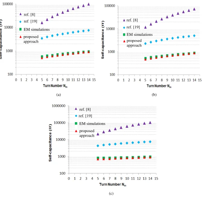
self-capacitances obtained by the CPS lines approach used in [8] and [19]. These results are presented in Fig. 14, where a good agreement of Cs with the simulated results can be observed. For BPSCs from
groups 1 to 3, the error of Cs regarding CsEM ranged between 0.044% and 13.070%. On the other hand,
the calculation of self-capacitances by CPS lines presented in [8] generated values between 22 and 110 times higher than CsEM, because in [8] the voltage drop along the spiral winding as well as the
degeneration factors were not taken into account. Thus, comparing results described in Fig. 14 and Fig. 8, the study presented in [8] is more suitable for the determination of mutual capacitances than for self-capacitances, although the error was still higher than 30% for mutual capacitances. In [19], which also used the approach of CPS lines, it was already considered the voltage drop per turn, but an arbitrary degeneration factor equal to was adopted resulting in self-capacitances between 2.8 and 8 times greater than CsEM.
Brazilian Microwave and Optoelectronics Society-SBMO received 14 May 2018; for review 14 May 2018; accepted 20 Jun 2018
(a) (b)
(c)
Fig. 14. Plots of self-capacitance versus Nm for BPSCs (a) from group 1, (b) from group 2 and (c) from group 3: for Cs using
CPW lines and degeneration factor approaches adopted in this paper, for CsEM using EM simulations and by modeling of
CPS lines used in [8] and [19].
So far all the inductance and capacitance analysis described in this section has neglected the influence of the underpass tracks. However, in order to determine the total parasitic capacitance Cp, it
is necessary to estimate the stray capacitance Cov.
The capacitance Cov, shown in Fig. 9, which arises between tracks of the BPSC’s top layer and
underpass tracks, can be estimated by equation
(37)
where (38) is the total area of all pairs of tracks overlapping between the top layer and underpasses, being the width of the underpass track fixed at 0.25 mm for all BPSCs studied in this paper in order to minimize the impact of Cov about the total stray capacitance Cp. The effect of fringing fields is taken
ref. [8]
ref.[19]
EM simulations
proposed approach
ref. [8]
ref. [19]
EM simulations
proposed approach
ref. [8]
ref. [19]
into account by the fitting factor obtained by electromagnetic simulations which value, for each group of BPSCs, is described in Table VI.
TABLE VI. COEFICIENT
GROUP
1 8.83
2 10.95
3 10.27
Equation (37) is valid for the groups of BPSCs described in Tables I to III with a maximum error of 10% regarding the Cov obtained by EM simulation.
After determining Cov by means of the equation (37) and Cs using equation (34), the total parasitic
capacitance Cp of each monofilar winding of the BPSC is then determined by equation (32).
III. METHODOLOGY, RESULTS AND DISCUSSIONS
A. Methodology
In order to validate the lossless model and the theory presented in the previous section, three double-sided BPSCs on FR-4 substrate, coated with solder mask were manufactured. The common specifications of these BPSCs are defined in Table IV and the individual specifications of each one are set in Table VII.
TABLEVII.MANUFACTUREDBPSCS N BIFILAR w(mm) s(mm) Doutb(mm) Dinb(mm)
20 BPSC-1 0.80 0.20 49.80 10.20 24 BPSC-2 0.55 0.20 55.30 19.70 28 BPSC-3 0.55 0.45 65.55 10.45
BPSCs with 20, 24 and 28 turns were manufactured, so that the first resonances (peak and valley) may be a frequency spectrum measurable by the Keysight (Agilent) 4294A precision impedance analyzer.
Tables were made with the main electrical parameters of the BPSC in order to establish a comparative analysis between the results obtained by the proposed model, by EM simulation as well as for values measured by the 4294A impedance analyzer, for the three BPSCs described in Table VII.
The electrical parameters of the lossless model were obtained according to the theory presented in section II and by an algorithm implemented in MATLAB [20].
1. Simulated Parameters
Parameters Cp, Ls and M were obtained by EM simulations (Method of Moments – MoM) using
Brazilian Microwave and Optoelectronics Society-SBMO received 14 May 2018; for review 14 May 2018; accepted 20 Jun 2018
impedance matrix or to a Y admittance matrix. After determination of Ls and M, the simulated
magnetic coupling factor k can be determined by applying equations (40) and (41) in equation (14). The capacitance Cp is obtained by the equation
(39)
being the angular frequency where the first resonance peak occurs and Ls and M are determined
by the equation
(40)
and
(41)
considering the BPSC as a quadripole (port 1 formed by terminals 1-2 and port 2 formed by terminals 3-4 of the BPSC) and and are elements of the impedance matrix Z of the quadripole.
The simulated capacitance Cs is also determined in the same way described above for Cp using
equation (39), but the simulation must be done without the underpass tracks and simulated Cov, which
in turn, is obtained by subtracting Cp from Cs.
In order to obtain simulated Cm, the layout of each BPSC was drawn in the Keysight ADS with a
short circuit between terminals 1-2 of the PSC B1 and also in the terminals 3-4 of the PSC B2 aiming to minimize the influence of the Rp-Cp and Ls-Rs branches on the simulated Cm. Next, a single port was
connected between B1 and B2 windings of the BPSC, and later, the S parameter matrix was converted into a Y admittance matrix.
Thus,
(42)
For comparative analysis with the electric parameters obtained for the model, Cp and Cm values
obtained by EM simulation were determined at 1 MHz, because the manufacturer of the FR-4 substrate and the solder mask provide this test frequency for the dielectric constant as well as for the loss tangent. Ls, M and k were also obtained at 1 MHz which is a region that provided stable values of
inductances, since this frequency is relatively distant from the first resonance valley f1v of each BPSC analyzed.
2. Measured Parameters
Cm, Ls and M were measured according to the experimental procedure described by [22] for coreless
planar transformers. In order to obtain measured Cm, a short circuit between terminals 1-2 of the PSC
B1 and also in the terminals 3-4 of the PSC B2 are done for reasons already described in the previous subsection. Value measured of Ls was obtained between terminals 1-2 and with terminals 3-4 in
polarity terminals 2-3 of the BPSC were initially short-circuited and the inductance L14 seen by the terminals 1-4 was measured. Subsequently, the short circuit was removed between terminals 2-3. Next, terminals 2-4 of the same polarity were connected and the inductance L13 seen by terminals 1-3 of the BPSC was measured [22].
From the measured values of inductances L14 and L13, the mutual inductance M of the BPSC was determined using equation
(43)
After the determination of Ls, M and the measurement of the first resonance peak f1p, the capacitance Cp can be estimated using equation (5) and k, again, by equation (14).
The measurements of Cp, Cm, Ls, M and k were also obtained at 1 MHz for the same reason mentioned for the simulated parameters.
B. Results and Discussions
Tables VIII, IX and X show the main parameters (Cp, Cm, Ls, M, k, f1p and f1v) of BPSC-1, BPSC-2 and BPSC-3 obtained for the model, for the values measured by the impedance analyzer and by EM simulation. These tables also show, in the last two columns, the percentage difference or error of each modeled and simulated parameter regarding the measured values, where it is observed that the respective errors of all parameters of the proposed model are smaller than 10%.
TABLE VIII.BPSC-1: COMPARATIVE ANALYSIS
Parameters
Error (%) Model Measurement EM Simulation Model EM Simulation
Cp(pF) 1.2209 1.3199 1.2658 -7.5006 -4.0988
Ls(µH) 3.2527 3.4090 3.2839 -4.5849 -3.6697
M(µH) 3.0598 2.9354 2.9620 4.2379 0.9062
k 0.9407 0.8611 0.9020 9.2440 4.7497
Cm(pF) 111.1200 113.9120 118.9686 -2.4510 4.4390
f1p(MHz) 57.3296 55.0002 56.6039 4.2353 2.9158
f1v (MHz) 8.4066 8.2771 8.1705 1.5646 -1.2879
TABLE IX. BPSC-2: COMPARATIVE ANALYSIS
Parameters
Error (%) Model Measurement EM Simulation Model EM Simulation
Cp(pF) 1.3200 1.4327 1.3640 -7.8662 -4.7951
Ls(µH) 6.9997 7.1129 7.0033 -1.5915 -1.5409
M(µH) 6.6808 6.7250 6.5330 -0.6572 -2.8550
k 0.9544 0.9455 0.9328 0.9413 -1.3432
Cm(pF) 152.2700 156.8510 164.3389 -2.9206 4.7739
f1p(MHz) 37.4526 35.7500 37.0400 4.7625 3.6084
Brazilian Microwave and Optoelectronics Society-SBMO received 14 May 2018; for review 14 May 2018; accepted 20 Jun 2018
TABLE X. BPSC-3: COMPARATIVE ANALYSIS
Parameters
Error (%) Model Measurement EM Simulation Model EM Simulation
Cp(pF) 1.4513 1.4650 1.4564 -0.9352 -0.5870
Ls(µH) 7.5795 7.8754 7.7170 -3.7573 -2.0113
M(µH) 7.2545 7.2387 7.0320 0.2183 -2.8555
k 0.9571 0.9192 0.9112 4.1232 -0.8703
Cm(pF) 132.2000 130.1400 135.9030 1.5829 4.4283
f1p(MHz) 34.3014 33.8250 34.3400 1.4084 1.5225
f1v (MHz) 5.0278 5.0188 4.9743 0.1793 -0.8867
The error for the modeled Cp was smaller than 8% for the three BPSCs of Table VII. This error is
related with the accuracy in the calculation of Cov and Cs, which in turn depends on the accuracy of
the degeneration factor curves and upon the precision of the modeled Cm, associated with equations
(31) and (34).
Regarding the error in the modeled Cm, it depends not only upon the accuracy during the calculation
of elliptic integrals, but also on the accuracy during the calculation of average length lav that, for
simplicity, excluded the first two and the last two tracks of BPSC so that the mutual capacitance could be modeled as the capacitance of a CPW line. The exclusion of these tracks causes an error in the calculation of capacitance Cm, but this error can be limited to 13% if lav / (Doutb + Dinb) ≥ 8 and
designing BPSCs with at least a dozen of turns or N ≥10. Considering that in this paper the three BPSCs were manufactured with N ≥20 and lav / (Doutb + Dinb) ≥ 18, this procedure ensured an error
of less than 3% in Cm regarding to the measured data.
The parameters Ls, M and k had errors smaller than 10% using equations (6) to (14).
The first resonances (peak f1p and valley f1v) of each BPSC, using equations (4) and (5), were estimated with an error of less than 5%.
Tables XI to XIII show Cov and Cs of the BPSC-1, BPSC-2 and BPSC-3 obtained both by the model
and by EM simulation. These tables also show, in the last column, the percentage difference or error of each modeled capacitance regarding the simulated values, where it is observed that the respective errors of those two capacitances for the proposed model are smaller than 5%.It is important to note that the fact that each monofilar winding have been designed with two underpass tracks has make the
Cov capacitance significant, representing more than 30% of the total parasitic capacitance Cp for the
Finally, because underpass tracks are essential for connecting the BPSC to the impedance analyzer, such tracks could not be extracted from the manufactured BPSC. Thus, it was not possible to measure
Cov and Cs which prevents a comparative analysis with the values modeled of Cov and Cs.
TABLE XI. BPSC-1: Covand Cs
Capacitance (pF) Model EM Simulation Error (%)
Cs 0.7409 0.7790 -4.8909
Cov 0.4800 0.4868 -1.3969
TABLE XII. BPSC-2: Covand Cs
Capacitance (pF) Model EM Simulation Error (%)
Cs 0.8594 0.9010 -4.6171
Cov 0.4606 0.4630 -0.5184
TABLE XIII. BPSC-3: Covand Cs
Capacitance (pF) Model EM Simulation Error (%)
Cs 0.8784 0.8780 0.0456
Cov 0.5729 0.5784 -0.9509
IV. CONCLUSIONS
In this paper an electrical model for the open square BPSC thatcovers the first valley and the first resonance peak for future applications as PSR sensor and WPT system was presented. The electrical parameters of the model were determined and a new approach was proposed to calculate mutual capacitances of BPSCs, based on CPW lines. In order to validate the proposed model, three BPSCs on FR-4 substrate and with solder mask were manufactured, tested on the impedance analyzer and also submitted to electromagnetic simulations. Subsequently, tables with the main electrical parameters were produced aiming to establish a comparative analysis between the results obtained with the proposed model, by EM simulation, as well as for the measured values. Finally, the parameters of the model were obtained with errors smaller than 10% and the first valley and the first resonance peak were determined with errors smaller than 5%, which showed good agreement with the data obtained in the analyzer impedance and by EM simulation.
REFERENCES
[1] N. Tesla, “Coil for electro-magnets,” U.S. Patent 512340, Jan. 09, 1894.
[2] W.C. Wysock, J.F. Corum, J.M. Hardesty and K.L. Corum, “Who Was The Real Dr. Nikola Tesla? (A Look At His Professional Credentials),” Antenna Measurement Techniques Association, pp. 1-5, Oct. 2001.
[3] C. M. de Miranda, “Equationing and modeling de Tesla’s bifilar coil and its proposal as a biotelemetric self-resonant
sensor,” M.S. dissertation, Dept. Electrical Engineering and Applied Computer Sciences, Federal Univ. of Technology
– Paraná (UTFPR), Curitiba, PR, Brazil, 2012 (in portuguese).
[4] A. Massarini and M. K. Kazimierczuk, “Self-capacitance of inductors,” IEEE transactions on power electronics, v. 12, n. 4, pp. 671-676, July 1997.
Brazilian Microwave and Optoelectronics Society-SBMO received 14 May 2018; for review 14 May 2018; accepted 20 Jun 2018
Congress of Biomedical Engineering (CBEB), v. 23, Porto de Galinhas, PE, Brazil, Oct. 2012 (in portuguese). [6] M. Ghovanloo and G. Lazzi, “Transcutaneous magnetic coupling of power and data,” in Wiley Encyclopedia of
Biomedical Engineering, M. Akay, Ed. Hoboken, NJ: Wiley, 2006.
[7] C. M. de Miranda and S. F. Pichorim, "A Self-Resonant Two-Coil Wireless Power Transfer System Using Open Bifilar Coils," IEEE Transactions on Circuits and Systems II: Express Briefs, vol. 64, no. 6, pp. 615-619, June 2017. [8] O. Isik and K.P. Esselle, “Design of monofilar and bifilar Archimedean spiral resonators for metamaterial
applications,” IET Microwaves Antennas & Propagation, vol. 3, n. 6, pp. 929-935, Oct. 2009.
[9] S. F Pichorim, V. A Marcis and G. T. Laskoski,“Humidity in sandy soil measured by passive, wireless, and resonant sensor with bifilar coil,” in First Latin-American Conference on Bioimpedance – CLABIO, Journal of Physics: Conference Series407, Joinville, SC, Brazil, Oct. 2012.
[10]D. D. Reis, T. E. Cervi and S. F. Pichorim, “Passive resonant sensor using bifilar coil for moisture measurement on
woods,” in MOMAG 2014: 16th SBMO - Brazilian Symposium on Microwave and Optoelectronics and 11th CBMag
-Brazilian Congress of Electromagnetism, Curitiba, PR, Brazil, pp. 198-203, Sept. 2014. (in portuguese).
[11]S. F. Pichorim, “Passive, wireless, resonant sensor with open bifilar winding,” Brazilian Patent Application 10 2013
008282-1 A2, April 05, 2013, in Revista da Propriedade Industrial, Rio de Janeiro, RJ, Brazil, no. 2320, p. 96, June 23, 2015. (in portuguese).
[12]J. Chen and J. J. Liou, “On-chip spiral inductors for RF applications: An overview,” Journal of Semiconductor
Technology and Science, v. 4, n. 3, pp. 149-167, Sept. 2004.
[13]S. S. Mohan, M. del Mar Hershenson, S. P. Boyd and T. H. Lee, "Simple accurate expressions for planar spiral inductances," IEEE Journal of Solid-State Circuits, vol. 34, no. 10, pp. 1419-1424, Oct. 1999.
[14]G. Ghione and C. U. Naldi, "Coplanar Waveguides for MMIC Applications: Effect of Upper Shielding, Conductor Backing, Finite-Extent Ground Planes, and Line-to-Line Coupling," IEEE Transactions on Microwave Theory and Techniques, vol. 35, no. 3, pp. 260-267, Mar 1987.
[15]R. N. Simons, “Coplanar Waveguide with Finite-Width Ground Planes,” in Coplanar Waveguide Circuits,
Components and Systems, New York: John Wiley & Sons, 2001, pp. 112-126.
[16]C.H. Wu, C.C. Tang and S.I. Liu, "Analysis of on-chip spiral inductors using the distributed capacitance model," IEEE Journal of Solid-State Circuits, vol. 38, n. 6, pp.1040-1044, June 2003.
[17]T. Masuda, A. Kodama, T. Nakamura, N. Shiramizu, S.Wada, T. Hashimoto, and K. Washio, “A simplified
distribution parasitic capacitance model for on-chip spiral inductors,” in Digest of Papers. 2006 Topical Meeting on Silicon Monolithic Integrated Circuits in RF Systems, San Diego, CA (USA), pp. 111-114, Jan. 2006.
[18]LAB Fit - Curve Fitting Software. Available: http://zeus.df.ufcg.edu.br/labfit
[19]J. Olivo, S. Carrara and G. De Micheli, “Modeling of printed spiral inductors for remote powering of implantable
biosensors,” in 5th International Symposium on Medical Information and Communication Technology, Montreux, Switzerland, pp. 29-32, Mar. 2011.
[20] MATLAB (Matrix Laboratory) software. Available: https://www.mathworks.com/products/matlab.html [21]Keysight Advanced Design System (ADS) software. Available: http://www.keysight.com/find/eesof-ads