ISSN 1941-7020
© 2009 Science Publications
Inverse Sine Phase Detector Phase Locked Loop Associated with Modified Multi
Band LC Quadrature Voltage Controlled Oscillator for Wireless
Communication Systems at 0.9, 1.8, 2.4, 3.5 GHz
Mahmoud Abdellaoui
National Institute of Electronics and Communications, Sfax, Tunisia
Abstract: Problem statement: In this study and in consequence of the restricted performance of the multi standard wireless receiver utilizing the classical architectures, we proposed and presented a new architecture of multi band wireless receiver based on an Inverse Sine Phase Detector Phase Locked Loop (ISPDPLL) associated with modified multi band LC quadrature Voltage Controlled Oscillator (VCO), supporting GSM/DCS/DECT/Bluetooth/WiMax systems. Approach: To accomplish the multi standard receiving architecture at sufficiently good performance and at a low hardware cost, the proposed circuit, using an ISPDPLL associated with VCO based on switched capacitors utilizing a several numeric controlled capacitive branch and cross-coupled transistors, was implemented in 0.35 µm CMOS technology and designed to yield quadrature output signals (I-Q) allowing to eliminate the dephasing block (90°) employed in a multi band Zero IF architecture receiver, that make the proposed architecture amenable for monolithic integration and 4G multi standard application. Results: This novel system presented high performance and good potentiality to cover perfectly the wireless multi standard receiving on the large band with the same transmission condition. Conclusion/Recommendations: The performance of this system was analyzed and demonstrated to have a minimum phase noise, a good Factor Of Merit (FOM) and wide tuning for these standard applications. Key words: Wireless receiver architecture, ISPD PLL, multi band LC quadrature VCO, phase noise,
tuning range, FOM
INTRODUCTION
Phase Locked Loop (PLL) is used widely in the implementation of modern systems, particularly in the field of communication applications. But, This PLL, called classical PLL, presents many disadvantages and limitations due especially by the loop filter which causes many problems such as aliasing effect and the limitation of bandwidth because if the filter bandwidth is decreased, the capture process became slower, the capture range decreases and the lock up time increases. In the other hand, the aim problem for the standard PLL is the phase error/phase noise. Many studies are developed to reduce phase error and phase noise by the addition of feedback loops[1]. In this way, the standard PLL can be tuned by first designing the transient and steady state of a second-order PLL and then taking care of the working operation under steady frequency (third order) and frequency ramps (fourth order).
Those including eluded because it is very complex. Anything else, the conventional PLL stay to operate in a wide hold range with important phase error and higher phase noise’s due to employ three loop filters. For thus, a new architecture of the PLL is proposed,
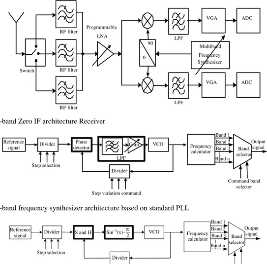
called Inverse Sine Phase Detector Phase Locked Loop (ISPDPLL). The ISPDPLL is a PLL structure without using any filters and the phase detector and the loop filter used generally in the standard PLL are replaced by a Inverse Sine Phase Detector (ISPD) including a track and Hold circuits (T/H), an inverse converter and a Voltage Controlled Oscillator (VCO)[2-4]. The suppressed filter in the ISPDPLL makes the system able to operate in a large band frequency without using any gain block and minimizes the lock up time of the circuit. The ISPD is the useful way to enhance the limitation of the locking range of the conventional PLL[2]. To accomplish the multi band receiving architecture (Fig. 1) at a low hardware cost, many propositions are presented based on:
limited range of the variable capacitance of the varactor, the tuning range of CMOS LC VCOs is very small. Hence[6] proposed that the varactor was controlled by the DC potentials at both of its input terminals to enable the LC VCO yielding a wide tuning range. Fong[7] developed the accumulation MOS varactor to provide wide band tuning capability at a low supply voltage. However, many studies explore the tuning range of LC VCO but may not meet the multi band requirement
• An ISPDPLL multi band synthesizer with frequency calculator is proposed herein to achieve a low phase noise with a narrow tuning range for GSM / DCS and WiMax systems (Fig. 3). This multi band synthesizer using the ISPDPLL architecture associated with frequency calculator block responsible to generate all the frequency bands and three numeric controlled blocks which
control the band selection, the steps selection in the selected band and the variation of the step selected and that’s why the different band are usually didn’t have the same characteristics. The frequency calculator, which be conceived by a combination of a frequency operators like dividers and multipliers, allows to translate the frequency generated by the ISPDPLL to the frequency range of the desirable band. The step selection and the variation of the step selected was conceited by programmable dividers[8]. Owing to the limited covering range of the operators (doubler or divide by 2), the frequency range of the multi band wireless receiver and especially the tuning range of the VCO is very small. However, many studies explore the tuning range of VCO with a low phase noise, but may not meet the multi band requirement
LPF
LPF 90
0 Programmable
LNA
Multiband Frequency Synthesizer
VGA
VGA
ADC
ADC RF filter
RF filter
RF filter Switch
Fig. 1: Multi-band Zero IF architecture Receiver
Phase detector
Divider Divider
Step variation command Step selection
Frequency calculator
Band 1 Band 2 Band 3
Band n Band selector
Command band selector
Output signal Reference
signal
LPF
VCO Gain
Fig. 2: Multi-band frequency synthesizer architecture based on standard PLL
S and H VCO
Divider Divider
Step variation command Step selection
Frequency calculator
Band 1 Band 2 Band 3 Band n
Band selector
Command band selector
Output signal Reference
signal Sin
−1 (x)-
2
π
To overcome this drawback, the ISPDPLL using the multi band LC quadrature VCO is proposed to achieve a wide tuning range with low phase noise/phase error and supporting many bands of the wireless communication. Improvements about the wireless receiver structure consist particularly to merge or to unit the dephasing block (90°), used generally in the multi band Zero IF architecture receiver, with the VCO allowing obtaining a unit cell called multi band LC quadrature VCO which associated with ISPDPLL.
MATERIALS AND METHODS
The aim of this research is to give a clear and concise exposition of the proposed system operating cycle. This provide sufficient detail to allow the work to be repeated by the others. In this research, we presented and described a detailed of the design of the novel synthesizer based on ISPDPLL associated with a modified multi band LC quadrature VCO to insist on an originality of the system and his performance.
Synthesizer based on ISPDPLL associated with a modified multi band LC quadrature VCO: To face the enormous demand of mobile multi media applications with a very high data rates, the 4G front-end transceiver needs a high performance which can be obtained mainly with an optimal architecture and a multi band VCO[9-11]; for thus, our idea, in this study, is to associate and to combine the ISPDPLL with a modified LC quadrature VCO for multi standards application. This modification reside to generate a separated bands (two bands for GSM900, one band for DCS1800-UMTS-Bluetooth and one band for WiMax: the VCO can cover the GSM standard at two separate bands (from 0.83-0.938 and 0.943-1 GHz) and the DCS/DECT/Bluetooth standards at one band (from 1.69-2.21 GHz) and the WiMax fixed standard also at one band (from 2.27-3.5 GHz) (Fig. 4) by using a several numeric controlled capacitive branches but not employed a binary weighted like[12-16], to enlarge the frequency coverage according the desired band. Also, the main object, in this study, is to combine the advantages of the ISPDPLL[2] and the advantages of the multi band LC quadrature VCO[12] indeed to conceive a new architecture of multi band frequency synthesizer supporting GSM/DCS/UMTS/Bluetooth and WiMax. In the other hand, improvements, about the wireless receiver structure, using the new architecture, consist to merge or to unit the dephasing block with the LC quadrature VCO allowing to obtain a simples and a robustness circuit.
Fig. 4: Frequency oscillation vs. control voltage with switching combinations
System description: ISPDPLL with LC quadrature VCO: The proposed multi-band synthesizer using ISPD associated with multi band quadrature LC VCO and two digital controlled blocks which control the steps selection in the selected band and the variation of the step selected to make the synthesizer able to operate at different bands, is shown in Fig. 5. The system consists of ISPDPLL associated with a modified multi band LC quadrature VCO (LC QVCO).
Recall to the ISPDPLL is a PLL structure without using any filters and the phase detector and the loop filter used generally in the standard PLL are replaced by an Inverse Sine Phase Detector (ISPD) including a track and hold circuits, an inverse sine converter and a quadrature voltage controlled oscillator using the LC Tank (LC QVCO). The key assumptions and approximations of the ISPD involved with employing the mathematical description of the ISPD characteristics. A new mathematical model of the ISPD characteristic is already studied and designed in previous study[2,4] and given as:
( )
(
)
( )
f x =a 1 x+ − 1 x− +c x (1)
With
( )
1
3
1 2
c x = × + ×a x a x
Where: a = 1.37 a1 = -0.37
S and H
Multi band VCO
Divider Divider
Step variation command Step selection
Band3 Reference
signal
Sin
−1(x)
-2
π
Command band selector
Band1 Band2
Band n
Fig. 5: Architecture of the proposed multi-band frequency synthesizer
Fig. 6: ADS Simulation’s diagram of the ISPD
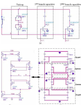
Figure 6 shows the ADS simulation’s diagram of the mathematical model of the ISPD. The suppressed filter in the ISPDPLL makes the synthesizer able to operate in a large band frequency without using any gain block and minimizes the lock up time of the circuit. This structure became completely integrated in the same wafer. The LC QVCO is designed to include cross-coupled transistors, switched capacitors, spiral inductors and varactor. The QVCO using LC tank is choose herein to achieve a low phase noise and low hardware cost for multi band applications. This QVCO can produce quadrature signals at different centred frequencies at a shared circuit block with the minimized overhead to support multi standards. According to these commonly used standards, the GSM, DCS-UMTS-bluetooth and WiMax have centred frequencies of 0.9, 1.8, 2.4 and 3.5 GHz. So, the conception of the proposed synthesizer is reduced to conceive and optimize the Multi-Band VCO which will determine the performance of the Local Oscillator circuit. The adaptation of the LC VCO architecture, for the GSM/DCS/DECT/Bluetooth and WiMax application, reside mainly on the determination of the number of switched capacitors branches needed to cover all the desired bands and the capacitors values. The modified LC quadrature VCO core consists of two cells (one in
Fig. 7: Transistor scheme of the multi band LCQVCO: (a): Resonator circuit; (b): Active circuit of each cell; (c): Equivalent scheme for the parasitic capacitance extraction
Design and analysis of the system: In order to surpass the risk of the worst coverage of the minimal frequency band (GSM), we chose to divide the GSM coverage in two under-bands: The first can cover the uplink frequency range and the second can cover the downlink frequency range. Therefore, we need generate four bands: The first to cover the WiMax standards (2.5-3.5 GHz), the second to cover the DCS/DECT/Bluetooth standards (1.71-2.4 GHz), the third and the fourth to cover respectively the uplink and the downlink bands of the GSM standard. Besides, in order to optimize the LC QVCO architecture, both the varactor circuit, using of two capacitive branches is sufficient to cover four frequency bands, since the numeric command voltage «vc1» and "vc2" can take four numeric combinations, knowing that the low and the high logical states are respectively equivalent to 0V and 3V. Concerns Our conception’s algorithm, we start with sizing the active circuit according to constraints of 0.35 µm process technology as supply voltage and the polarization current, after that we conceive the resonator circuit calibrated to cover the maximal frequency band (WiMax), then we pass to size the switching capacitances in order to assure the coverage of the minimal frequencies band (GSM).
To minimize the corner frequency of 1/f3 phase noise, the active circuit (negative resistance) is indispensable to have a symmetrical CMOS structure with the identical Trans conductance on the PMOS and NMOS transistors[17].
In the other hand, the grid Length (L) must be in general the smallest possible to decrease the thermal noise and to increase the transition frequency of the transistor (either L = 0.35 µm),
The main constraint imposed on the sizing of the varactor circuit, it is that it must allow the coverage of the largest frequency band, so, the capacitance variation of the varactor can determined by:
WiMax DCS/ DECT / UMTS var
GSM ,B1 GSM,B2
C , C ,
C max
C , C
∆ ∆ ∆ ≥ ∆ ∆ (2)
where, ∆CWiMax is the needed capacitance variation to
cover the WiMax band; that is similar with
∆CDCS/DECT/UMTS, ∆CGSM,B1 and ∆CGSM,B2.
The Inversion mode (I-MOS) and the accumulation mode (A-MOS) varactor structures present many advantages compared to the MOS structure like a wide and monotonous capacitance variation[16], but the choice of the structure A-MOS involved replacing the p+ diffusions by a n+ diffusions, that impose a technology constraints. Then, in order to conceive a flexible and adaptable circuit by all technologies, it is amenable to use the I-MOS varicap structure.
In our application, we used a varactor structure composed by two PMOS transistors which each function’s in I-MOS capacitance. This structure offers more stability opposite to the temperature effects[18].
The sizing of the two branches capacitances is can deduced by calculating the maximal total capacitance value needed (Ctotal,max), including the parasitic
capacitances of the active circuit and the minimal total capacitance value needed (Ctotal,min), including the
parasitic capacitance of the active circuit (CMOS) and the
varactor capacitance (CVar):
total var sw1 sw 2 mos
C =C +C +C +C (3)
According to the Fig. 7c, the parasitic capacitance of the active circuit (CMOS) can be approximately by:
mos p,pol n ,pol p,mos n ,mos
C =C +C +C +C (4)
With:
Cp,pol and Cn,pol = The equivalent capacitance of the
PMOS and NMOS polarization stages
Cp,MOS and Cn,MOS = The equivalent capacitance of the
differential CMOS structures So, by determine the equivalent capacitance variation of the two branches, the sizing of the first branch must switch the VCO from the WiMax band to the DCS/DECT/UMTS band and the sizing of the second capacitance branch must switch the LC quadrature VCO from the DCS/DECT/UMTS band to the GSM band.
One of the main challenges of multi band synthesizer design based on ISPDPLL associated with modified LC quadrature VCO is to extend the narrow tuning range without degrading noise performance; for thus, we should minimized the corner frequency of 1/f3 phase noise versus foffset allowing obtaining a lowest
intersection frequency range between 1/f2 and 1/f3 ( f1/f
3
/foffset is neglected). In this case, the phase noise
performance of the proposed multi band circuit is simulated, which integrates the following expression:
2 osc offset
dis offset
K T f f
PN(f ) 10log 1
P 2Qf
Ν Β
α ∆
= × + (5) Where:
αN = The noise factor
kB = Boltzmann’s constant
T = The absolute temperature
Pdis = The power dissipation at the resonator part
Table 1:Phase noise and fom simulated values of the proposed circuit Frequency Phase noise FOM
Bands GHz @1 MHz @1 MHz
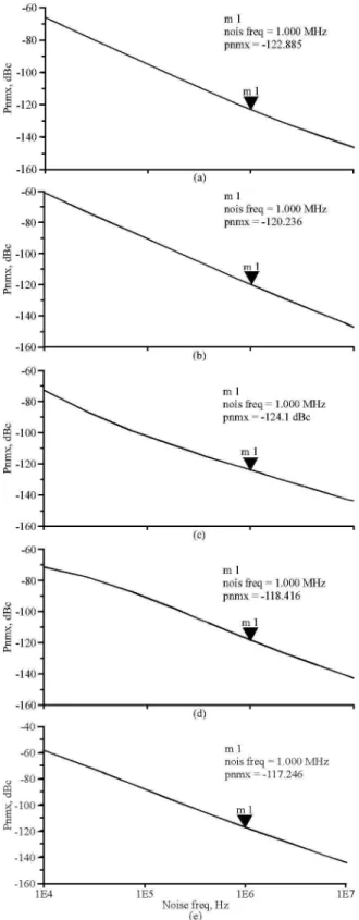
WiMax 2.3 -137 dBc -196 dB 3.5 -128 dBc -186 dB DCS/UMTS/… 1.7 -125 dBc -189 dB 2.1 -118 dBc -187 dB GSM 0.8 -122 dBc -180 dB 1.0 -119 dBc -179 dB
In Eq. 5:
1
osc var sw1 sw 2 MOS
f = π[2 [L(C +C +C +C )]]− (6) With:
CSW1/2 = The equivalent first and second cell
capacitance value Cvar = The varactor capacitance
Usually, Figure Of Merit for the VCO is defined as[7]:
offset dc
osc offset
FOM PN(f ) 10log(P / 1mW) 20log(f / f )
= +
− (7)
where, PDC is the DC power consumption of the QVCO.
RESULTS AND DISCUSSION
In this research, we was taken as application the Multi standard wireless receiver based on ISPDPLL associated with a modified multi band LC quadrature VCO. Then, we summarized the major results in relation to any hypotheses advanced in this study. Discussed these results and compared with the literature references.
To study the performance of the system suggested, we determine its phase noise, Figure Of Merit, lock up time, keep/capture range and tuning range, as well as the output spectrum at all standards according to several parameters such as resonator’s components sizes. For the analysis, the circuit dissipates 10.3 mA from a 3V supply. The Inductor was set to 15 pf; the varactor, the first capacitive branch and the second capacitive branch for each cell were set to (200 µm / 30 µ m), (10 pf / 100 µ m / 10 m) and (10 pf / 225 m / 30 m). The phase noise and Figure Of Merit of the system for all standards were summarized in the Table 1. Table 1 shows the simulated values of phase noise and Factor Of Merit (FOM) (using Fong expression[7]) of the proposed circuit at 1MHz Offset frequency, at the different generated bands. As can be seen in these results, the best phase noise of the proposed multi band circuit is-137dBc at 2.3GHz and the best FOM is -196 dB. The phase noise at all standards is shown in Fig. 8a-e.
(a)
(b)
(c)
Fig. 9: Lock up time simulation of the circuit suggested at: (a): WiMax Band; (b): DCS band; (c): GSM band
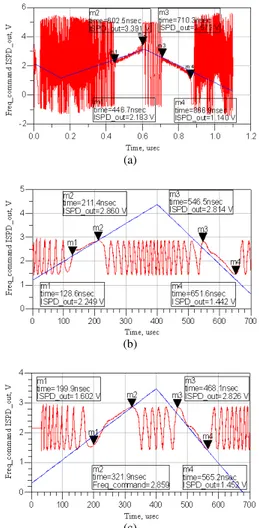
To show the improvement made by the system suggested, we have carried out a comparative study with a system based on standard PLL and classical VCO. The results obtained show that the lock up time of the system suggested is better than the other systems. Knowing that the lock up time of the system based on the classical PLL/VCO is in order of 30 ns[19], the lock up time of the system suggested at the WiMax band is 8ns (Fig. 9a-c). It is noticed that with configuration, the tuning range is wider than that of the system using standard PLL and classical VCO (78% versus 54%), which confirms that when the lock up time is better, the capture/keep range is larger and the tuning range is wide. According to Fig. 10a-c, the keep and capture range are higher than that of the system with standard PLL and classical VCO (0.7/1.4 GHz versus 100/ 380 MHz).
(a)
(b)
(c)
Fig. 10: Keep/capture range simulation of the proposed circuit applied in: (a): WiMax band, (b): GSM band, (c): Bluetooth band
We can also notice that the keep and capture ranges are the important characteristics of the frequency synthesizer, they describe its frequency performance. Generally, the keep range is limited by the linearity of the VCO, whereas the capture range depends of the gain and the speed of the synthesizer. To simulate the keep and capture ranges of the proposed synthesizer, we varied the frequency of the input reference signal by using another VCO controlled by the "Freq_command" signal. According to the Table 1, we can conclude that the synthesizer, with its keep range, can cover the totality of all the desired bands (GSM/UMTS/DCS/DECT/WiMax) with a good and large capture range.
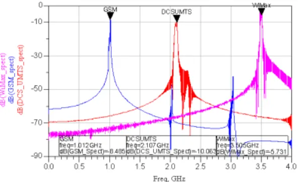
Fig. 11: Spectrum simulation of GSM/DCS-UMTS and WiMax at maximum frequency synthesized
Fig. 12: Spectrum simulation of GSM/DCS/WiMax at minimum frequency synthesized
results show that by using the frequency synthesizer based on ISPD PLL without any filters and without any controlled gain block, we can cover the GSM/DCS/DECT/Bluetooth/WiMax bands with a good performance and a wide band frequency range, that make the proposed architecture receiver based on ISPD PLL amenable for monolithic integration and multi-band application.
CONCLUSION
Due to the good performance of the modified multi-band LC quadrature VCO, the frequency synthesizer architecture based on ISPD PLL presented high performance and good potentiality to cover GSM/DCS/DECT/Bluetooth and WiMax bands. Moreover, the simplicity of this architecture allows saving area and power in favor of 4G programmable single chip-multimode-very high scale integration.
REFERENCES
1. Carlosena, A. et al., 2007. Design of high order phase lock loops. IEEE Trans. Circ. Syst. II: Express Briefs, 54: 9-13.
http://ieeexplore.ieee.org/xpl/freeabs_all.jsp?arnum ber=4063458
2. Mahmoud, A., B. Gassara and N. Masmoudi, 2007. A new model of an inverse sine phase detector to design ISPD PLL demodulator without using any filters. AEUE-Int. J. Elect. Commun., 61: 10-21. DOI: 10.1016/j.aeue.2006.01.007
3. Seon, J.K., 2000. Analysis and conception of PLL circuit using a phase detector. Thesis at High National School of Telecommunications. Paris-France.
4. Mahmoud, A., B. Gassara and N. Masmoudi, 2005. Integrated wide band FSK demodulator based on ISPD PLL. Proceeding of the 3rd International Conference on IEEE-NEWCAS, June 19-22, IEEE Xplore Press, USA., pp: 407-410. http://ieeexplore.ieee.org/xpl/freeabs_all.jsp?arnum ber=1496745
5. Hwang, J.T. et al., 1999. Wide tunable CMOS multiple-nested-feedback ring type LC oscillator.
Elect. Lett., 35: 144-145.
http://ieeexplore.ieee.org/Xplore/login.jsp?url=/iel4 /2220/16345/00758022.pdf?arnumber=758022 6. Razavi, B., 1997. A 1.8GHz CMOS voltage
controlled oscillator. Proceeding of the IEEE International Conference on Solid State Circits, Feb. 6-8, San Francisco CA., USA., pp: 388-389. http://ieeexplore.ieee.org/xpl/freeabs_all.jsp?arnum ber=585453
7. Fong, N. et al., 2003. Design of wide band CMOS VCO for multiband wireless LAN applications. IEEE J. Solid State Circ., 38: 1333-1342. http://ieeexplore.ieee.org/Xplore/login.jsp?url=/iel5 /4/27322/01214726.pdf?temp=x
8. Bilel, G., M. Abdellaoui and N. Masmoudi, 2007. 4G wireless receiver architecture based on ISPD PLL supporting GSM/DCS and WiMax. Proceeding of the 4th International Multi-Conference on Systems, Signals and Devices, March 19-22, Hammamet-Tunisia, SHAKER-VERLAG Publishers, Germany and ISBN: 978: 9973959065, pp: 59-62.
9. Lin, Y.B. and I. Chlamtac, 2001. Wireless and mobile Network architecture. John Wiley and Sons.
10. Li, X. and M. Ismail, 2002. Multi-Standard CMOS Wireless Receivers: Analysis and Design. 1st Edn., Springer Publishers, USA., ISBN: 10: 1402070322, pp: 168.
12. Hsia, M.L. et al., 2006. A multi band CMOS LC
quadrature VCO for
GSM/DCS/DECT/WCDMA/Bluetooth systems. Proceeding of the 1st International Symposium on Wireless Pervasive Computing, Jan. 16-18, IEEE
Xplore Press, USA., pp: 1-4.
http://ieeexplore.ieee.org/xpls/abs_all.jsp?arnumbe r=1613637
13. Hajimiri, A. and T.H. Lee, 1999. The Design of Low Noise Oscillators. 1st Edn., Springer Publishers, USA., ISBN: 10: 0792384555, pp: 224. 14. Hajimiri, A. et al., 1999. Design issues in CMOS differential LC oscillators. IEEE J. Solid-State
Circ., 34: 717-724.
http://ieeexplore.ieee.org/Xplore/login.jsp?url=/iel4 /4/16453/00760384.pdf?temp=x
15. Seung, O.M. et al., 2003. A 74%, 1.56-2.71 GHz, Wide-Tunable LC-Tuned VCO in 0.35 m CMOS technology. Microwave Optic. Technol. Lett.,
37: 98-100.
http://cat.inist.fr/?aModele=afficheN&cpsidt=1469 1746
16. Craninckx, J. et al., 1997. A fully integrated spiral-LC CMOS VCO set with prescaler for GSM and DCS-1800 systems. Custom Integrated Circuits Conference. Proceeding of the IEEE, May 5-8, pp: 403-406. DOI:10:1109/CICC.1997.606654 17. Thierry, L., 1992. Conception and modelling of
oscillators and their Phase Locked Loop mobile radiocommunication applications. THESIS at High Engineering School of Poitiers-France
18. Dalenda, B.I., 2006. Design of perfect oscillator for mobile radio. Masters of Electronics, National Engineering School of Sfax-Tunisia. ID: 2006-77. 19. Razavi, B., 1997. A 2 GHz, 1.6 mW PLL. IEEE J.