978 Brazilian Journal of Physics, vol. 36, no. 3B, September, 2006
Nanocrystalline GaN and GaN:H Films Grown by RF-Magnetron Sputtering
D. M. G. Leite∗, A. L. J. Pereira, L. F. da Silva, and J. H. Dias da Silva Laborat´orio de Filmes Semicondutores, Depto de F´ısica,
Universidade Estadual Paulista, 17033-360 - Bauru-SP, Brazil
Received on 8 December, 2005
The structural and optical properties of nanocrystalline GaN and GaN:H films grown by RF-magnetron sputtering are focused here. The films were grown using a Ga target and a variety of deposition parameters (N2/H2/Arflow rates, RF power, and substrate temperatures). Si (100) and fused silica substrates were used at relatively low temperatures (Ts≤420K). The main effects resulting from the deposition parameters variations
on the films properties were related to the presence of hydrogen in the plasma. The X-ray diffraction analysis in-dicates that the grain sizes (∼15nm) and the crystallized volume fraction significantly decrease when hydrogen is present in the plasma. The optical absorption experiments indicate that the hydrogenated films have absorp-tion edges very similar to that of GaN single crystal films reported in the literature, while the non-hydrogenated samples present larger absorption tails encroaching into the gap energies.
Keywords: GaN; GaN:H; Nanocrystalline; Sputtering; Hydrogenation
I. INTRODUCTION
Gallium nitride films received considerable attention in the last years due to their applications in optoelectronic devices [1,2]. Several reports are found for different material struc-tures: single crystal [2-4], nanocrystalline [5,6], and amor-phous [7]. Most studies refer to film preparation onto differ-ent substrates due to the difficulties concerning the growth of GaN bulk crystals [2-4].
Recently, Guo et al. [8] have successfully grown single crystal GaN films at relatively low substrate temperatures us-ing the RF-magnetron sputterus-ing, brus-ingus-ing considerable inter-est to the preparation using this technique. The sputtering technique is versatile for making possible the deposition of a large variety of films on different types of substrates over large areas and at relatively low temperatures. The simplicity of the sources used, the wide variety of materials addressed, the low cost, and the generation of fewer residues than some traditional methods, are among the advantages of the tech-nique.
The effect of hydrogenation/de-hydrogenation of GaN was analyzed by several authors, but the analysis are almost [6] completely restricted to the passivation of defects and impuri-ties in single crystal GaN films [9,10].
In this study was reported the preparation of nanocrystalline GaN and GaN:H thin films grown by RF-magnetron sputter-ing with different deposition parameters (N2/H2/Ar flow rates, RF power and substrate temperatures). The effects of some deposition parameter variations on the film properties were analyzed by X-ray diffraction and optical absorption. The main results were related to hydrogen incorporation.
II. EXPERIMENTAL DETAILS
The films were prepared in a RF-magnetron sputtering setup specially assembled to grow III-V compound semicon-ductor films [11]. The system used electronically controlled gas flow, total pressure, and RF power (at 13.6 MHz). The
knife-edge metal seals and turbomolecular pumping allowed residual pressures were better than 1x10⁻⁵Pa before deposi-tions. Fig 1 shows the schematic representation of the sputter-ing chamber.
FIG. 1: Schematic representation of the sputtering chamber geome-try and main components: 1-Water cooling; 2-Heating resistors; 3-Substrates; 4-Ga target; 5-Permanent magnets; 6-Shield; 7-Insulator; 8-RF cable; 9-Thermocouple; 10-Gas inlet; 11-Pumping system.
The 350 mm diameter chamber shelters a central magnetron target holder of 100 mm diameter (Fig. 1). The distance be-tween the target surface and the substrate was 50 mm during all the depositions.
D. M. G. Leite et al. 979
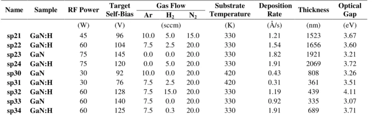
TABLE I: Deposition parameters and the optical gap of GaN and GaN:H films deposited by reactive RF-magnetron sputtering. The total pressure in the chamber was kept constant at 2.0 Pa. The optical gap was set as the energy in which the absorption coefficient is 104cm−1.
Gas Flow Name Sample RF Power Target
Self-Bias Ar H2 N2
Substrate Temperature
Deposition
Rate Thickness
Optical Gap
(W) (V) (sccm) (K) (Å/s) (nm) (eV)
sp21 GaN:H 45 96 10.0 5.0 15.0 330 1.21 1523 3.67
sp22 GaN:H 60 104 7.5 2.5 20.0 330 1.54 1656 3.60
sp23 GaN 75 145 0.0 0.0 20.0 330 1.82 1921 3.21
sp24 GaN:H 75 120 0.0 5.0 20.0 330 1.91 2069 3.72
sp30 GaN 30 92 10.0 0.0 20.0 420 0.43 808 3.26
sp31 GaN:H 30 76 7.5 2.5 20.0 420 0.31 361 3.51
sp32 GaN:H 60 128 7.5 15.0 20.0 330 1.19 439 4.11
sp33 GaN 60 140 7.5 0.0 20.0 330 0.92 335 3.07
sp34 GaN:H 60 125 7.5 0.3 20.0 330 1.91 689 3.71
silica-SiO2)were used simultaneously. The substrate temper-ature was measured by a thermocouple located at the depo-sition face of a fused SiO2substrate and it was 420K for the samples sp30 and sp31, and was 330K for all others samples. Table I shows the other deposition parameters and the optical gap of each sample.
The structural characterization was performed by X-ray dif-fraction at grazing (3 ˚ ) incidence andθ-2θdetection
geom-etry. The diffractometer (Rigaku – Ultima+ 2000) uses a CuKα1 radiation (1.54056 ˚A). The Scherrer’s formula [12]
was used to roughly estimate the mean crystallite sizes, with-out any further refinement. The atomic force microscope (AFM) measurements were performed in air. A Park Sci-entific Instruments AutoProbe CPsetup was used in contact mode with a 20nm diameter silicon tip.
The optical normal incidence transmittance and near nor-mal (8o off-normal) reflectance spectra were measured in
the 190-900nm range in a Varian Cary-1 spectrophotometer equipped with integrating sphere apparatus. The spectropho-tometric data were used to calculate the refractive index, ab-sorption coefficient and film thickness, according to computer routines based on existing methods [13,14].
III. RESULTS
The obtained films presented good adherence to the sub-strate and good optical homogeneity. The surface roughness was analyzed by AFM (Fig. 2). By comparison with results reported for other materials [15], the observed surface rough-ness was associated to a quenched growth regime [15]. In this regime the adsorbing species do not have sufficient mobility on the surface during film growth to soften the surface. The resulting statistical roughness is probably due to the relatively low ratio of substrate temperature to the GaN melting temper-ature (Ts/Tmelt∼0.17) and also to the low kinetic energy of the adsorbing species. The low kinetic energy is due to the moderate RF power/accelerating bias potential used (Table I) and to the thermallization of the energetic Ga atoms ejected from the target by with collisions with the working gas
mix-ture.
FIG. 2: AFM image of a GaN:H/Si(100) sample (sp34). Observe that the base plane scales are much wider than the vertical scale.
Concerning the atomic arrangements of the film mater-ial, the X-ray diffraction patterns, Fig.3, indicates that the non-hydrogenated GaN film grown on amorphous SiO2have a considerable crystallized volume fraction. The observed diffraction peaks indicate that the crystallites of the non-hydrogenated material have mean grain sizes of the order of 15 nm, wurtzite structure (α-GaN), and a tendency of
prefer-ential growth of the (0002) planes. Very similar results were observed for our films grown on Si (100) substrates. In this case the only difference is that the films grown on Si gener-ally presented slightly stronger (∼15-20%) peaks, indicating a weak tendency to be more crystallized than the ones grown in amorphous silica (SiO2)substrates.
tempera-980 Brazilian Journal of Physics, vol. 36, no. 3B, September, 2006
ture (420K), and with samples sp33 (non-hydrogenated) and sp32/sp34 (hydrogenated), prepared under lower RF and dif-ferent H2gas dilutions, a similar trend was observed: the non-hydrogenated films exhibit diffractograms compatible with a significant amount of crystallization, while the diffractograms of hydrogenated samples are almost completely broad indi-cating amorphous characteristic. It is important to emphasize that this was valid even for the smaller H2dilution fraction al-lowed by our setup (sp34). So, concerning the resulting struc-tural characteristics of the samples, the presence of hydrogen had the higher influence among all the deposition parameters.
FIG. 3: X-ray diffraction patterns of the sp23 (non-hydrogenated) and sp24 (hydrogenated) samples grown onto amorphous silica sub-strates.
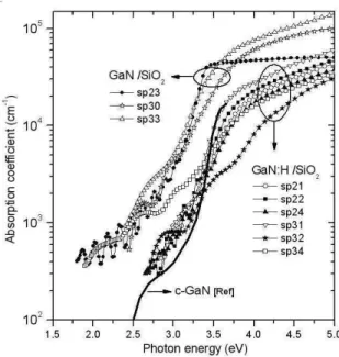
The transmittance and reflectance spectra of the films dis-played a very regular set of interference fringes in the trans-parent and weakly absorbing spectral regions indicating good optical homogeneity of the films, and allowing good precision (∼5%) in the determination of optical constants. The cal-culated absorption coefficient curves in the absorption edge spectral region are displayed in Fig. 4. It is apparent from this figure that the set of non-hydrogenated samples can be distinguished of the set of hydrogenated curves, the curves in each group being similar to each other. This evidences that the effect of the presence of hydrogen on the optical absorption overcomes the effects of the variation of other deposition pa-rameters, similarly to what was already observed in the struc-tural characterization. The analysis of the absorption curves indicated that the non-hydrogenated samples are more absorb-ing in the whole spectral region studied, except only for the low absorption part of the less hydrogenated sample (sp34). Also, with this exception, the absorption characteristics of the set of hydrogenated samples were very similar the one corre-sponding to GaN single crystal [4].
IV. DISCUSSION
Considering the effect of the variations of the deposition parameters on the structural and optical properties of the sam-ples, it was noted that the presence of hydrogen has a much
]
FIG. 4: Absorption edges of the GaN films. A reference edge of a single crystal GaN grown by MOCVD [4] was included for compar-ison.
stronger effect than other deposition parameters, namely: RF power, substrate kind (c-Si and a-SiO2), substrate tempera-ture (330/420K), and presence of Argon in the plasma, within the ranges used in this work. The effective presence of bonded hydrogen in the films was confirmed by infrared transmittance spectra (FTIR), which display strong absorption bands asso-ciated to the N-H stretching vibration centered at∼3200cm−1 and N-H bending vibrations at∼950cm−1. Based on a-SiN:H oscillator strength data [16], a rough estimation of the N-H bond density was carried in the hydrogenated GaN films. This estimation indicated that the percent N-H bond concentration can be as high as a few tens in the more hydrogenated samples. No systematic change in the growing rate or refractive index was observed in association with this relatively high hydrogen incorporation.
crys-D. M. G. Leite et al. 981
tallite grain boundaries or internal surfaces of voids and in the nearby amorphous regions.
Finally, it was noticed that the samples having higher crys-tallized fraction (the non-hydrogenated set) had also higher optical absorption above the gap energy than the amorphous set (hydrogenated samples). This fact deserves consideration since in the crystallized material the selection rules for crys-talline momentum conservation would apply, and would lower the absorption for energies far from the singularity position, as compared to amorphous material. Nevertheless the small crystallite dimensions can severely interfere in the applica-tion of the symmetry selecapplica-tion rule due to the low dimension, and can produce severe lattice distortions and defects that are probably present. Also the creation of the defects in the crys-tallite grain boundaries and nearby amorphous regions would enhance the overall disorder in the material, producing the higher absorption. In this way, the lower absorption of the hydrogenated (predominantly amorphous) samples indicated a reduction of the overall disorder in the material.
Further work is necessary to a more complete understand-ing of the role of the deposition parameters on the films prop-erties.
V. CONCLUSION
GaN and GaN:H films were prepared at low substrate tem-peratures (TS≤420K) using the reactive RF-magnetron
sput-tering technique. Among the deposition parameters: different N2/H2/Ar gas mixtures, RF power, substrate kind (Si (100), a-SiO2), and substrate temperatures (330/420K), the stronger effect observed on structural and optical properties was related to the presence of hydrogen in the plasma gas mixture. The presence of hydrogen in the plasma, even in small quantities, significantly reduces the crystallized fraction and crystallite sizes (in the nanometer scale range). Hydrogenation is also associated to an increase of the optical gap and a reduction of optical absorption at lower energies. The observed effects are indirect indications that the presence of hydrogen is proba-bly related to an overall defect density reduction in crystallite grain boundaries and internal surfaces of voids in the GaN films produced by reactive sputtering.
Acknowledgements
We acknowledge Prof. Mˆonica Alonso Cotta and Jo˜ao Her-mes Clerice (SPM/LPD laboratory, Unicamp) for the AFM measurements and Prof. Margarida Juri Saeki and Prof. L´ıgia de Oliveira Ruggiero for the use of the FTIR and UV-Vis spectrophotometers respectively. This work was supported by FAPESP.
[1] S. J. Pearton (ed.).GaN and Related Materials. Gordon Breach Science Publishers, Amsterdam, 1997, 538p.
[2] S. C. Jain, M. Willander, J. Narayan, R. Van Overstraeten. Jour-nal of Applied Physics87, 965 (2000).
[3] S. J. Pearton, C. R. Abernathy, M. E. Overberg, et.al. Journal of Applied Physics93(1), 1 (2003).
[4] S. Strite and H. Morkoc¸. Journal of Vacuum Society and Tech-nology B10(4), 1237, (1992).
[5] J. Kim and P. H. Holloway. Journal of Vacuum Society and Technology A22(4), 1591 (2004).
[6] T. Miyazaki, K. Takada, S Adachi, and K. Ohtsuka. Journal of Applied Physics97,093516 (2005).
[7] S. B. Aldabergenova, A. Osvet, G. Frank, H. P. Strunk, P. C. Taylor, and A. A. Adreev, Journal of Non-Crystalline. Solids 299-302, 709 (2002).
[8] Q. X. Guo, A. Okada, H. Kidera, T. Tanaka, M. Nishio, and H. Ogawa, Journal of Crystal Growth237, 1079 (2002).
[9] S. Nakamura, N. Isawa, M. Senoh, and T. Mukai. Jpn. Journal of Applied Physics31, 1258 (1992).
[10] S. J. Pearton.The role of hydrogen in GaN and related
com-pounds. In:GaN and Related Materials. S.J. Pearton (ed.). Gor-don Breach Science Publishers, Amsterdam, 1997. Chap. 11, pp. 333-369.
[11] A. L. J. Pereira, J. V. Lopez, and J. H. Dias da Silva, Revista Brasileira de Aplicac¸˜oes de V´acuo22(2), 50 (2003).
[12] B. D. Cullity, S. R. Stock.Elements of X-Ray Diffraction, 3rd edition, Prentice-Hall, Inc., New Jersey, 2001, 664p.
[13] J. I. Cisneros. Applied Optics37, 5262 (1998).
[14] J. I. Cisneros, G. B. Rego, M. Tomyiama, et al. Thin Solid Films 100(2), 155 (1983).
[15] J. A. Thornton. Journal of Vacuum Society and Technology11 (4), 666 (1974).
[16] A. Morimoto, I. Kobayashi, M. Kumeda, and T. Shimizo. Japanese Journal of Applied Physics25 (9), L752 (1986). [17] The ESR characterization of GaN and GaN:H samples were