626 Brazilian Journal of Physics, vol. 34, no. 2B, June, 2004
Hall Effect in InAs/GaAs Superlattices with Quantum Dots:
Identifying the Presence of Deep Level Defects
R.M. Rubinger*, G.M. Ribeiro
†, A.G. de Oliveira
†, H.A. Albuquerque
†,
R.L. da Silva
†, W.N. Rodrigues
†, and M.V.B. Moreira
†∗
Departamento de F´ısica e Qu´ımica, Instituto de Ciˆencias, Universidade Federal de Itajub´a, Caixa Postal 50, 37500-903, Itajub´a, Brazil
†
Departamento de F´ısica, Instituto de Ciˆencias Exatas, Universidade Federal de Minas Gerais, Caixa Postal 702, 30123-970, Belo Horizonte, MG, Brazil
Received on 27 March, 2003
We have carried out van der Pauw resistivity and Hall effect measurements on a series of Molecular Beam Epitaxy InAs/GaAs superlattice samples containing InAs quantum dots. Three growth parameters were varied, the InAs coverage, the number of repetitions of the InAs/GaAs layers, and the GaAs spacer thickness. The results can be grouped in two sets, those samples presenting low and high resistivity. The group presenting low resistivity is composed by the samples with GaAs spacer of 30 monolayers (ML) and InAs coverage of 1.9 monolayers. The group presenting high resistivity is composed of samples with GaAs spacer of 40 ML. We claim that the high resistivity characteristic is due to the presence of deep level. Increasing the spacer from 30 to 40 ML decouples the InAs planes favouring the deep level formation.
1
Introduction
Quantum dots (QD) are quasi-zero-dimensional structures and should behave in some aspects like conventional point defects. InAs QD forms on GaAs due to the lattice mis-match between both materials. Besides the electronic states of the QD itself, deep states related to the InAs layers and QD have also been reported by some researchers [1].
In this work we performed Hall measurements on InAs/GaAs QD in order to investigate the formation of such deep levels, which are standard characteristic of high resis-tive samples due to their high activation energies.
2
Experimental details
We have grown samples stacking InAs/GaAs by Molecular Beam Epitaxy (MBE). The samples were grown on semi-insulating Liquid Encapsulated Czochralsky (LEC) GaAs substrates. A 1µm GaAs buffer layer was grown at a
sub-strate temperature of 600o
C. After that the growth tempera-ture was reduced and kept between 495oC and 530oC during
the InAs/GaAs growth. Three parameters were intention-ally varied, namely, the InAs coverage, GaAs spacer thick-ness, and the number of periods of InAs/GaAs. Two GaAs spacer thickness of 30 and 40 monolayers (ML) were used. The InAs coverage varied between 1.4ML and 3.0ML. The growth parameters are summarized in Table 1.
Table 1. The growth parameters.
Sample Growth Temp. (o
C) # InAs InAs coverage (ML) GaAs Thick (ML)
9821 500 1 1.9 30
9822 530 5 1.9 30
9823 510 10 1.9 30
9826 510 50 1.9 30
9827 510 50 1.9 40
9829 510 50 2.0 40
9832 495 50 2.5 40
9833 510 50 3.0 40
R.M. Rubingeret al. 627
The contacts were deposited on the surface of the sam-ple in a van der Pauw geometry. For this we used small In drops and backed the contacts in a N2:H285:15 reducing at-mosphere at 300oC for 10 minutes. The van der Pauw
mea-surements followed the same procedures of Look [2]. The measurements were carried in darkness. For low resistive samples it was possible to measure from room temperature down to 3.9K, while for high resistive samples the lowest temperature was around 250K.
3
Results
We obtained the Hall density n and the resistivity ρ as a
function of the temperature. For obtaining these parame-ters the sample was considered as a two-dimensional elec-tron gas (2DEG). The samples can be grouped in two sets according to their electrical characteristics, either high or low resistivity values. We will assign them as group #1 and group #2 respectively. Group #1 is composed by samples 98-21, 22, 23, and 26. Group #2 is composed by samples 98-27, 29, 32, 33 and 9902.
Figure 1 shows the planar densitynas a function of
tem-perature for the group #1. It presents the same behavior for all samples. It decreases slightly with the temperature, hav-ing a minimum in the range between 15K and 60K and in-creases for further decreasing of the temperature. This is a typical 2DEG signature.
Figure 1. Thenfunction for group #1.
Figure 2 presents the resistivity results for group #1, measured in units ofΩ[], where [] stands for adimensional unit since the electron gas is confined in two dimensions. The resistivity values are in the range of 4x10⁴
Ω[] to 2x10⁷ Ω[].
Figure 2. The resistivity function for group #1.
The resistivities decrease for increasing temperatures reaching a minimum around 100K and then increase slightly for further temperature elevation.
Figure 3 presents the planar n for the group #2.
Al-though there is no 2D signature for this group this was carried to compare with results of group #1. All samples present the same behavior, increasingnfor increasing
tem-perature. The 2D free carrier density is ofntype and
tem-perature dependent measurements give activation energies between 0.4 eV and 0.6 eV. These values are too high to be related to an electronic state of InAs QDs, which are in the order of 0.2eV [3,4].
Figure 3. Thenfunction for group #2.
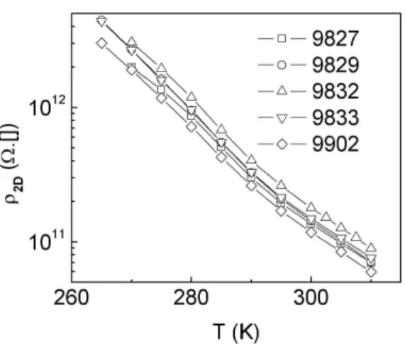
Figure 4 presents the resistivity results for group #2. The resistivity values are in the range of 5x10¹⁰
Ω[] to 5x10¹²
628 Brazilian Journal of Physics, vol. 34, no. 2B, June, 2004
Figure 4. The resistivity function for group #2.
4
Discussion
The experimental results confirm the differences between group #1 and #2. It is also important to note that group #1 is composed of samples with 30 ML GaAs spacers, and group #2 is built with the 40 ML GaAs spacer samples.
Since the samples are quite similar concerning the growth parameters, we claim that deep levels in group #2 explain the differences. Indeed, the temperature dependence and the electric characteristics of group #2 which scales with activation energies between 0.54eV and 0.60eV can be ex-plained based on the presence of deep levels.
There are three main factors, which would explain the formation of deep levels in our samples. The first factor is related to the 7% lattice mismatch between InAs and GaAs, which induces the formation of self-assembled quan-tum dots (SAQD) when the InAs coverage is higher than the critical value of 1.65ML. The strained GaAs layer might re-sult in the presence of deep levels, as have been previously reported [4-6]. The second factor is the growth tempera-ture. Low growth temperatures contribute to the formation of deep level defects [7]. All insulating samples were grown at 510o
C (except the sample #9832 that was grown at 495o )
which is well above 400o
C and, in turn, results in negligi-ble deep level formation in pure GaAs samples. For such growth temperatures the strain reaches deep into the GaAs layer. This contribute to the formation of deep levels. The third factor is the stacking of layers. It is well known that stacking another InAs layer closer to a first one induces the formation of vertically coupled quantum dots [8]. However, recent works [4-5] indicate another effect of stacking lay-ers, the reduction of the formation of deep levels by lattice relaxation.
All samples of group #2 have a nominal GaAs layer thickness of 40ML, a number of superlattice repetitions of 50, a growth temperature of 495o
C or 510o
C, and InAs coverage between 1.40ML and 3.00 ML. We claim that al-though the GaAs layer is thin enough to allow the formation
of vertically coupled quantum dots it is beyond a critical thickness responsible for the deep level inhibition.
Group #1 has four samples with the GaAs layer thick-ness of 30ML. For samples 9821, 9822, 9823 and 9826 the effect of stacking seems to be efficient to inhibit deep defect formation.
5
Summary
In this work we have measured Hall effect and resistivity in self-assembled quantum dots samples. Some of them show deep level defect characteristics. We identified that stacking layers of InAs spaced by GaAs layers of 30ML thick inhibits the deep level defect formation.
A GaAs spacer layer thickness of 40ML is enough to preserve the vertically coupled quantum dots [8]. It is known that the proximity of InAs layers plays an important role in deep level inhibition [1]. In our case, although 40ML is not thick enough to decouple the vertically alignment of QD it proved not to be efficient in inhibiting the deep level forma-tion. Under the used growth conditions, there might be a critical value for the GaAs layer thickness between 30 and 40 ML above which the inhibition of deep levels becomes ineffective.
Acknowledgements
We would like to acknowledge the Brazilian agencies CNPq, CAPES and FAPEMIG for financial support.
References
[1] C.J. Park, H.B. Kim, Y.H. Lee, D.Y. Kim, T.W. Kang, C.Y. Hong, H.Y. Cho, and M.D. Kim, J. Crys. Growth 227-228, 1057 (2001).
[2] D.C. Look in: Electrical Characterization of GaAs Materials
and Devices, Wiley, New York, 1989.
[3] C. Walther, J. Bollmann, H. Kirsme, W. Neumann, and T. Masselink, Appl. Phys. Lett. 76, 2916 (2000).
[4] C. Walther, J. Bollmann, H. Kirsme, W. Neumann, and T. Masselink, Phys. B 273-4, 971 (1999).
[5] L. D´ozsa, Zs.J. Horv´ath, Vo Van Tuyen, B. P¨odor, T. Moh´acsy, S. Franchi, P. Frigeri, E. Gombia, and R. Mosca, Microelectron. Engineer. 51-52, 85 (2000).
[6] R.M. Rubinger, J.C. Bezerra, E.F. Chagas, J.C. Gonzalez, W.N. Rodrigues, G.M. Ribeiro, M.V.B. Moreira, and A.G. de Oliveira, J. Appl. Phys. 84, 3764 (1998).
[7] N.N. Ledentsov, M. Grundmann, N. Kirstaedter, O. Schmidt, R. Heitz, J. Bohrer, D. Bimberg, V.M. Ustinov, V.A. Shchukin, A.Y. Egorov, A.E. Zhukov, S. Zaitsev, P.S. KopEv, Z.I. Alferov, S.S. Ruvimov, A.O. Kosogov, P. Werner, U. Gosele, and J. Heydenreich,
Sol.-Stat. Electron. 40, 785 (1996).
[8] J.C. Gonz´alez, F. M. Matinaga, W.N. Rodrigues, M.V.B. Moreira, A.G. de Oliveira, M. I. N. da Silva,.J. M. Vilela, M. S. Andrade, D. Ugarte, and P. C. Silva; Appl.Phys.Lett.,