Inuene of Annealing on the Optial and Eletrial
Properties of Multilayered InAs/GaAs Quantum Dots
A. J. Chiquito,Yu. A.Pusep, S. Mergulh~ao,Y. Galv~aoGobato,and J.C. Galzerani
Departamentode Fisia, UniversidadeFederalde S~aoCarlos,
CP676,13565-905, S~aoCarlos,SP,Brazil
Reeivedon23April,2000
Theharateristisofmulti-layeredInAs/GaAsselfassembledquantumdots(SAQDs)annealed
af-terthegrowthwereherestudiedusingaombinationofapaitane-voltage(C-V)measurements,
Ramansattering and photoluminesene(PL)spetrosopy. Theombinationof theresults
ob-tainedwiththethreetehniques,gaveevidenesthattheannealing at500 o
Causesthesharpness
oftheSAQDsinterfaes, whiletheannealingat600 o
CeliminatedtheSAQDs. However,the
om-parisonwiththease ofsinglelayeredSAQDs,revealedathermalstabilityofthelastsystemeven
atanannealing temperatureof700 o
C,thusonrmingthe roleoftheinterlayerstraininthelow
temperaturediusionproess.
Theharateristisofmulti-layeredInAs/GaAsself
assembled quantum dots (SAQDs) annealed after the
growth were here studied using a ombination of
apaitane-voltage(C-V)measurements,Raman
sat-tering and photoluminesene (PL) spetrosopy. For
that, sampleswith dierentSi doping levelsof the
re-gions where the dotswere grown were prepared. The
ombinationoftheresultsobtainedwiththethree
teh-niques, gaveevidenes that theannealing at
tempera-tureslosetothegrowthtemperatureausesthe
sharp-nessoftheInAs/GaAsinterfaesintheSAQDssystem,
while the annealing at 600 o
C eliminated the SAQDs.
However,theomparisonwiththeaseofsinglelayered
SAQDs,revealedathermalstabilityofthelastsystem
evenat anannealing temperatureof 700 o
C, thus
on-rmingtheroleoftheinterlayerstraininthelow
tem-peraturediusionproess.
Theontrolofthehomogeneityoftheself-assembled
quantum dots (SAQDs) is of fundamental importane
when theappliationof these struturesin tehnology
isonsidered. Besidestheattemptsdoattainthe
homo-geneity throughthe deposition rate and the substrate
temperatureontrol,apost-growthannealinghasalso
beenattemptedasavalidtoolin reentworks[1-4℄. In
this ase, the homogenization was supposed to our
due to the atomi inter-diusion proess between the
barriersandtheislands(dots),whihhangesthesizes
andtheshapesofthedots. However,itisnotyetlear
howimportantaretherelativemodiationsofthe
in-terfaesand thebulkoftheSAQDs attainedafter the
annealing.
layered InAs/GaAs SAQDs strutures annealed after
thegrowth,wethenusedaombinationof
apaitane-voltage (C-V) measurements, and Raman and
photo-luminesene(PL) spetrosopies. TheC-V
measure-mentsbeingsensitivetotheeletronipropertiesofthe
studied systems(asthe PLspetrosopydoes), in
ad-ditiongiveinformationabouttheirloaleletroni
be-havior,whilethephononRamansatteringisawidely
reognizedstruturalsensitivetool.
Thesamplesweregrownbymoleular-beamepitaxy
on(100)GaAshighlydopedsubstrates. FiveInAs
lay-erswith nominal thikness2.3 monolayers(ML)
sepa-rated by 15 ML of bulk GaAs were grown at 450oC.
Thetransitionfromastreakedto aspottyhigh-energy
eletron diration (RHEED) pattern, observed after
1.8MLthikInAswasdeposited, indiatedthe
forma-tion of the 3D islands. After the growth of SAQDs,
anundopedGaAsseparatinglayer(25nm)wasgrown,
followedbyan undoped GaAs/AlAs (1 nm/3nm)
su-perlattie, in order to inrease the impedane of the
samples. WeusedsampleswithtwodierentSidoping
levelsoftheGaAs regionswherethe dotsweregrown:
sampleA hasN A
D
= 110 17
m 3
and sampleB has
N B
D
=110 17
m 3
. The post-growthannealing
pro-esswasdone in anargonatmosphere, for 20min. at
dierenttemperatures.
For omparison, the eets of annealing were also
studiedinasingle-layerSAQDssystem.
The C-V measurements were made using a
stan-dard lok-in tehnique (with a SR530 Stanford
T64000 triple spetrometer supplied with a CCD
de-tetorooledbyliquidnitrogen,whileforthePL
mea-surementsaSpex500Msinglespetrometerwitha
pho-tomultipliertubewasused. Allthemeasurementswere
madeat10K.
150
160
170
180
190
200
0.0
0.5
1.0
1.5
2.0
Sample A
(a)
N
CV
(10
18
cm
-3
)
150
160
170
180
190
200
0.0
0.1
0.2
0.3
0.4
0.5
0.6
0.7
z (nm)
(b)
Sample A,500
o
C
600
o
C
1.0
1.2
1.4
0.7
0.8
0.9
1.0
1.1
1.2
1.3
1.4
T = 10 K
B
A
600
o
C
PL intensity
(arb. units)
Energy (eV)
(c)
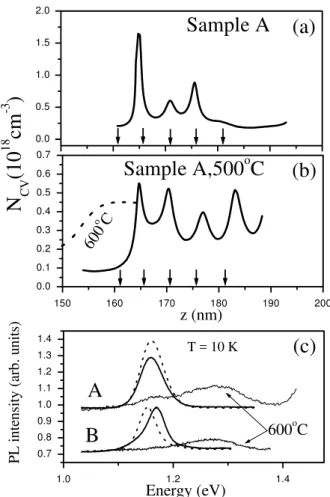
Figure1.As-grownandannealedC-Vprolesofthesample
Aareshowedinpanels(a)and(b). Panel()showsthePL
spetraoftheas-grownmultilayersamplesAandB(dotted
lines) taken at 10 K.The orresponding spetra after the
annealingat500 o
Careshownbyfulllines. Theurveswere
shiftedup forlearnessandthe exitationenergywas 2.70
eV.
The spatial distribution of the eletronsalong the
growthdiretionwasalulatedbytheusualequations
fortheC-Vproledetermination [5℄. Fig. 1(a)depits
theC-VproleofsampleA,fromwhihitispossibleto
notie the individual ontributions of the InAsplanes
ontainingthe dots,loatedat thefollowingdistanes
from thesurfae: 164 nm, 170 nmand 175nm. The
positionsofthepeaksareinaordanewiththe
nom-inal loalizations oftheseond, third andfourth InAs
planes(indiatedbyarrowsin Fig. 1). TherstInAs
layer does not ontribute to the C-V prole (in this
andalsoinsampleB),beauseitwasalreadydepleted
bythebuilt-ineldproduedbytheShottkyontat.
After annealing at 500oC [Fig, 1(b)℄, the InAsplanes
homogeneous. Similar results with the low
tempera-ture annealing were observedin sampleB (not shown
here). After theannealing at 600oC,the C-V proles
of both samples did not present any peuliarities
re-lated to theSAQDs, asdepitedby thedotted line in
Fig. 1(b) asan example; this is arst evidene that
the dots have disappeared after the seond annealing
proess(at600 o
C)inthese multi-layeredsamples.
TheorrespondingPLspetraofthesamplesare
de-pitedin Fig. 1(). Nosigniantinuene ofthelow
temperature annealing in the properties of the whole
multilayerSAQDssystemwasobserved,ontrarytothe
signiantmodiation in theindividual propertiesof
thelayersmeasuredbyC-V.However,astrong
modi-ationofthePLspetraafterannealingatahigher
tem-perature (600 o
C)was observed: the intensities of the
lines assoiated withthe SAQDs drastiallydereased
andanewblueshiftedbroadlineappearedaround1.3
eV.
260
280
300
0
2
3
5
7
8
10
sample
700
o
C
control
600
o
C
LO
TO
B
A
200
220
240
260
0
1
2
3
4
5
(a)
sample
control
700
o
C
Ram
an Intensity (arb. units)
600
o
C
B
A
DALA
TO(InAs)
(b)
Raman Shift (cm
-1
)
Figure 2. Raman spetra ofthe both multilayerand
on-trolsamples(singlelayerSAQDs). Panels(a)and(b)show
theRamanspetrameasuredinthefrequenyrangeofthe
InAs and GaAs phonons, respetively. The full and
dot-tedlines represent thesamplesannealedat 500 o
Candthe
as-grownsample, respetively;thethinlineswereobtained
after theannealing at600 o
C. Inthe bottomof the gure,
theRamanspetraofboththeas-grownandtheannealed
The Raman spetra of the samples with the two
dierent doping levels are shown in Fig. 2(a) for the
frequeny rangeoftheInAs optialphonons. Thefull
andthedottedlinesrepresentthesamplesannealedat
500 o
C andtheas-grownsample, respetively;thethin
lines were obtained after the annealing at 600 o
C. In
thebottonofthegure,theRamanspetraofboththe
as-grownandtheannealed(700 o
C)single-layerSAQDs
samples are presented. Following our previous
expe-riene, the line observed at 250m-1 was assigned to
theInAsTOphonon,whilenoontributionwasfound
at thefrequenieswhere theInAs LOphonon was
ex-peted [6℄. The weak line observed at 212 m 1
is
muhprobablyadisorderativatedlongitudinal
aous-ti(DALA)phononofGaAs. Sinenosigniantshift
of the bulk-lineInAsphonon frequeniesafter
anneal-ing at 500 o
Cwasobserved,weonludethat thebulk
strutureoftheSAQDswasnotyethangedbythelow
temperaturetreatment.
We also performed the Raman spetra in the
fre-quenyrangeoftheGaAs optialphonons[Fig. 2(b)℄.
The drawing lines have the same meaning as in Fig.
2(a). In this ase, both the LO and the TO bulk
phonons were learly deteted. Inthe as-grown
sam-ples, theirfrequeniesare red-shifteddue tothestrain
in the GaAs barriers. The absene of the bulk LO
phonons of the GaAs substrate (despite the fat that
the multi-layer SAQDsthiknesses are only25 nm) is
attributed to the inhomogeneity in these strutures,
that results in a strong elasti sattering of the light.
Asasupporttothishypothesis,theLOphononofthe
GaAs substrateappearedin thespetraafterthehigh
temperatureannealing (600 o
C),thus showing the
for-mationofanalloy(withoutmaro-defetslikethe
quan-tum dots) that would preventtheelasti satteringof
lighttoour. Inaddition,astrongontributionofthe
GaAs-likeoptialphonons withlargewavevetors,
re-eting theone-phonondensityofstates,wasdeteted
between the TO and the LO lines, for the low
tem-perature annealing. This defetindued Raman
sat-tering drastially dereases after annealing at 600 o
C;
thus, it seems that the multi-layer SAQDs aused a
strongviolationoftheRamanseletionrules(that
per-sists until after thelow temperature annealing),while
after thehigh temperatureannealing mostlythe
zone-enterphonons ontributesto thesattering, asa
fur-ther evidene that relativelyhomogeneous alloyswere
formed. Asamatteroffat,after annealingat 700 o
C,
theSAQDsdisappeared,andanIn
x Ga
1 x
Asalloywas
formed. As a result, the defet indued GaAs-like
were eliminated, while theGaAs bulk-like phonons of
thesubstratenowshowsup. Theshouldersdetetedat
thelowfrequeny sides of the LO Ramanlines
orre-spondtotheGaAs-likephononsofaIn
0;08 Ga
0;92 As
al-loy,onrmingtheaboverelatedobservationofthePL
measurements: the shiftedPL lines an beattributed
to an In
x Ga
1 x
As alloy with x =0;10formed asthe
resultoftheannealing.
So,it isworthnotiing thatthehomogenization of
theSAQDsandtheinreaseoftheloalizationof
ele-trons,observedbythe C-Vmeasurements,wasshown
toimply in strutural alterations, detetedby the
op-tialspetrosopies.
Contrarytothemulti-layerase,theRamanspetra
ofthesingle-layerSAQDsrevealed thepreseneofthe
InAsoptialphononsandtheGaAs-likedefetindued
modesassoiatedwiththedotsevenaftertheannealing
at700 o
C,asevidenedinFigs.2(a)and2(b). This
ob-servationisonrmedbythePLmeasurements(spetra
notshownhere): thelinesdue tothedotsarestill
ob-servedafter thehigh temperatureannealing,although
they are slightly blue-shifted and broadened. Thus,
fromthethreetehniqueshereemployed,weould
on-lude that the low temperature heat treatment (at a
temperature somewhat higher than the growth
tem-perature)resultsinadrastimodiationofthe
multi-layerSAQDs,while thesingle-layerstruture revealed
athermal stability even at rather high temperatures.
Webelievethat these observations onrm therole of
the interlayer strain in the low temperature diusion
proess.
Referenes
[1℄ R.Leon,Y.Kin,C.Jagadish,M.Gal,J.ZouandD.H.
J.Cokayne,Appl.Phys.Lett.69,1888(1996).
[2℄ A.O. Kosogov, P. Werner,U. Gosele, N. Bimberg, V.
M.Ustinov,A.Y.Egorov,A.E.Zhuokov,P.S.Kop'ev,
N. A. Bert, Z. I. Alferov, Appl. Phys. Lett. 69, 3072
(1996).
[3℄ S.Malik, C. Roberts, R. Murray and M. Pate, Appl.
Phys.Lett.71,1987(1997).
[4℄ S.Fahad,Z.R.Wasilewski,C.Ni.Allen,D.Piard,M.
Spaner, J.P.MCarey and P.G.Piva,Phys.Rev.B
59,15368(1999).
[5℄ E. H. Rhoderik and R. H. Williams,
Metal-semiondutorContats(Oxford, Cambridge)1988.
[6℄ Yu.A.Pusep,G.Zanelatto,S.W.daSilva,J.C.
Galz-erani, P. P. Gonzalez-Borrero, A. I. Toropov, and P.