Electroforming process in metal-oxide-polymer
resistive switching memories
Qian Chen1, Henrique L. Gomes1, Asal Kiazadeh1, Paulo R. Rocha1, Dago M. De Leeuw2, and Stefan C. J. Meskers3
1Center of Electronics Optoelectronics and Telecommunications (CEOT) Universidade do Algarve, Campus de Gambelas, 8000-139 Faro, Portugal,
2 Philips Research Labs, High Tech. Campus, 5656 AE Eindhoven, The Netherlands 3 Molecular Materials and Nanosystems, Eindhoven University of Technology, P.O. Box 513,
5600 MB Eindhoven, The Netherlands
Abstract. Electroforming of an Al/Al2O3/polymer/Al esistive switching diode is reported.
Electroforming is a dielectric soft-breakdown mechanism leading to hysteretic current–voltage characteristics and non–volatile memory behavior. Electron trapping occurs at early stages of electroforming. Trapping is physically located at the oxide/polymer interface. The detrapping kinetics is faster under reverse bias and for thicker oxides layers. Thermally detrapping experiments give a trap depth of 0.65 eV and a density of 5x10¹⁷ /cm2. It is proposed that the
trapped electrons induce a dipole layer across the oxide. The associated electric field triggers breakdown and ultimately dictate the overall memory characteristics.
Keywords: Resistive Random Access Memory (RRAM), electroforming soft-breakdown, non-volatile memory.
1 Introduction
Metal-Insulator-Metal (MIM) structures based on oxides shown resistive switching [1] properties and they are being considered interesting for the resistive random access memories (RRAMs) [2]. This simple diode structure, whose resistance can be programmed reversibly to be high or low, offers an interesting opportunity for application in high-density memory arrays, either as a memory [3] element in its own right or coupled to CMOS [4] addressing logic. One type offering excellent prospects is the metal-oxide-polymer diode Al/Al2O3/polymer/metal. Al2O3 [5] has been studied since 1962, when Hickmott [6] first reported that resistive switching occurs as a result of applied electric field. Studies of post-breakdown conduction in MIS capacitors were also preformed by Srivastaya and Bhattacharyya [7] using Al/Al2O3/Cds capacitors. Their sample exhibited bistable switching between two states in the post-breakdown stage, and they conclude that the conduction involved field ionization of traps [8] in both states. Later, Shatzkes, Av-Ron, and Anderson [9] studied the
post-breakdown conduction of thick (20-100nm) SiO2 films in metal-oxide-semiconductor (MOS) structures. They used Al/SiO2/Si and Cr/SiO2/Si capacitors and also obtained a controlled switching between two conduction states, the breakdown [10] being the change from the low to a high conductivity state. More recently, the study of the breakdown and post-breakdown conduction trough thin-oxide Cr/SiO2/Si capacitors also suggested that the breakdown could be understood as reversible change between two different conduction states. The nature of the defects [11] created during the soft-breakdown remains a matter of debate, for binary oxides such as TiO2 [12], ZrO2 [13], and Al2O3, it is commonly accepted that they are oxygen vacancies [14].
The objective of this study is to get insight into the early stages leading to a soft-breakdown or electroforming [15]. Evidences [16] are provided showing that breakdown is proceeded by electron trapping [17] at the oxide/polymer interface. The accumulated charge creates an internal electric field that eventually causes the rupture of the dielectric. Understanding the early stage of electroforming may allow us to optimize the electroforming procedure and fabricate resistive switching diodes with better memory characteristics. Furthermore, the role of the polymer layer in controlling the soft-breakdown mechanism [18] may be better understood.
2 Contribution to value creation
This study provides insight into the mechanism that changes a typical insulator material such as Al2O3 into an electrical bistable material interesting for RRAMs. The change in the electrical properties is caused by soft-breakdown process. The polymer layer added in series with Al2O3 plays a crucial role preventing thermal damage caused by Joule heating. Furthermore, it provides trapping sites that promote the establishment of a dipole layer across the oxide. The knowledge gained about the role of this dipole layer in controlling the dielectric breakdown will allow us to optimize the diode structure for non-volatile memory applications.
3 Device description
The diode structure shown in Fig. 1 consists of an Al bottom electrode, a sputtered layer of Al2O3 (20 nm), a spirofluorenepolymer (80 nm), and a Ba/Al (5 nm/100 nm) top electrode that forms an Ohmic contact with the polymer. The devices with an active area of 1 and 9 mm2 were encapsulated to exclude O2 and H2O. In all cases, positive bias voltage refers to the bottom Al electrode being positive with respect to the top Ba electrode. Current–voltage (J-V) curves were obtained using a Keithley 487 picoammeter.
4 Experimental results
The pristine devices were turned into programmable resistive switching memories by applying a 12 V voltage ramp as will be described in detail below. After this
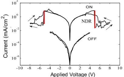
electroforming process, the devices exhibit bistable J–V characteristics and a negative differential resistance (NDR) region in the on-state, as shown in Fig. 2.
Fig. 1. (a) Schematic diagram showing the physical structure of the memory device, (b) photograph of an encapsulated device containing a number of diodes.
At room temperature, the memory can be switched between off- and on-state by applying voltage pulses with amplitudes corresponding to the top and bottom of the NDR. The device behaves as a non-volatile memory.
Fig. 2. J –V characteristics of the device in the off- and in the on-state.
Next we will focus on the electroforming process. Fig. 3 represents the electroforming of the diode. The bias voltage was swept at a ramp rate of 0.1V/s up to 10 V and the current density recorded with time. The J-V characteristic shows three distinct regions. In the first stage, region (I), for voltages in the range between 0 and 8 V, we observe a pronounced hysteresis in the current-voltage characteristics. In region (II), at bias voltages between 8 V and 10 V, the current rises exponentially with bias and is due to tunneling of electrons through the oxide. In this regime no hysteresis is observed. Finally in region (III), near 10 V, the current rises steeply and becomes noisy which are both typical characteristics of soft breakdown of the oxide. This process is irreversible; the electrical characteristics have changed permanently.
(a)
(b
)
-10 -8 -6 -4 -2 0 2 4 6 8 10 10-6 10-4 10-2 100 102 Voltage (V)C
ur
re
nt
(
m
A
/c
m
2)
ON OFF NDR 0 1 2 3 4 5 6 -5 0 5 10 15 20x 10 -9Applied Voltage (V)
C
ur
re
nt
(
m
A
/c
m
2)
s70321c3d3 0 1 2 3 4 5 6 -5 0 5 10 15 20x 10 -9Applied Voltage (V)
C
ur
re
nt
(
m
A
/c
m
2)
s70321c3d30
5
10
10
-1210
-1010
-810
-610
-4Applied Voltage (V)
C
ur
re
nt
(
A
/c
m
2)
IV
F1.M
III
I
II
The formed device behaves as a non-volatile memory as previously described in Fig. 2.
Fig. 3. Typical current-voltage characteristics during electroforming of Al/Al2O3/polyspirofluorene/Ba/Al diode.
To get insight into the mechanism we need first to understand the behavior in region (I). In the forward scan, the current increases with bias. However, in the backward scan the current is negligible. Actually the current level on the return scan is approximately equal to the displacement current associated with the device geometrical capacitance. If the subsequent J-V loop is recorded using the same bias conditions, the hysteresis is not present and the measured current equals the displacement current. Then, scanning forward to a higher bias voltage that has not been applied before, the current shows a large increase. Backward scans give the same low current value and are independent of the previous scans. The original hysteresis loops can be restored after resting for a few hours or days. These J-V loops are fully reversible. This behavior suggests that the observed hysteresis results from traps that fill in a time scale of seconds but empty slowly, on a time scale of hours. Since this process occurs only when negative bias is applied to the barium electrode, we propose that electrons injected by the barium electrode flow through the polymer layer and they accumulate at the oxide/polymer interface. The electrons must then be compensated by holes located in the aluminum electrode. When the charge build-up is high enough the associated electric field across the oxide layer forces a current (via Fowler–Nordheim or direct tunneling) through the oxide, this current create defects. When a critical defect density is reached the system breaks down and forms a percolation path of defects in the oxide.
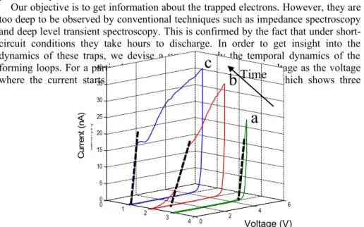
Our objective is to get information about the trapped electrons. However, they are too deep to be observed by conventional techniques such as impedance spectroscopy and deep level transient spectroscopy. This is confirmed by the fact that under short-circuit conditions they take hours to discharge. In order to get insight into the dynamics of these traps, we devise a way to study the temporal dynamics of the forming loops. For a particular J-V loop we defined an onset voltage as the voltage where the current starts to rise. This is illustrated in Fig. 4, which shows three
0 1 2 3 4 0 2 4 6 0 5 10 15 20 25 30 35 40 Applied Volatage (V) Forming loop C ur re n (n A ) O nset volta ge
a
b
c
Time
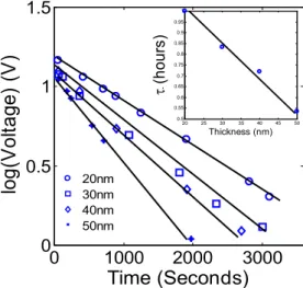
Voltage (V) Forming loop 0 2 4 6 8 10 10-10 10-9 10-8 10-7 10-6 10-5 10-4 Applied Voltage (V) C ur re nt ( nA ) IVF1.Mdifferent forming loops and how they involve with time. The intercept of the dashed line with the voltage axis is assumed to be the onset voltage. First the diodes are brought to a maximum onset voltage of 5 V. When the diode is left resting under short circuited conditions the onset voltage will move slowly with time to towards 0 V. The time dynamics of the onset voltage was monitored as function of time for different oxide thickness. The onset voltage follows an exponential behavior as function of time. Fig. 5 shows the logarithm of onset voltage as function of time for different
Fig. 4. Time dependence of the electroforming loops. A device electroformed to 5 V will approximately have the onset voltage of 5 V (curve (a)). By leaving the device resting in dark, the forming loop (a) will evolve to curve (b) and eventually (c). The onset voltage estimated by the intercept with the voltage axis (dash line) will decrease with time to below 1 V. oxide thickness. The thinner the oxide the slower is the recover process. The inset of Fig. 5 shows the relaxation time (τ) for different oxide thickness. It varies from 1 hour for a 20 nm oxide to 0.5 hour for a 50 nm thick oxide. Since the electrons must be neutralized by opposite charges at the aluminum electrode, the thicker the oxide layer the weak is the electric field associated with the dipole layer. This facilitates the trap emptying process.
In order to confirm that the electric field associated with the dipole layer favors the trapping of electrons, experiments were carried out under a reverse bias. When a reverse negative bias in the aluminum is applied compensating holes are forced out by the external bias. The accumulated electrons are no longer compensated by holes on the other side of the oxide layer. It is then expected that the emptying process should be faster.
Fig. 6(a) shows the change in onset voltage for a reverse field of -5 V to fully recover the J-V loop it takes approximately 100 seconds while under zero bias would take days to fully recover. Fig. 6(b) shows the recovery on onset voltage for increasing reverse bias under constant time (100s). The higher the reverse bias the larger is the onset voltage recover.
In order to obtain the trap signature the detrapping time constant have to be determined for different temperatures. These experiments are current under way. However, one of the simplest methods used to study deep traps in semiconductors is
the thermally stimulated conductivity (TSC) technique. In this experiment the traps are filled with the sample at low temperature then, upon heating, the trapped carries are released to the appropriate band and there is an increase in free carries density and hence in the conductivity. The amount of trapped charge is finite, being determined by the number of traps, and as the temperature is increase further all the trapped carriers are eventually released. Since excess carriers in the bands recombine the conductivity eventually falls, so there is a peak in a plot of the conductivity change as a function of temperature. The temperature at which this peak occurs is
Fig. 5. Semi-log plot of the onset voltage as function of time for different oxide thickness. Inset shows that relaxation time constant (τ) decreases linearly with the oxide thickness.
Fig. 6. (a) Change in onset voltage as function of time when a reverse voltage (-5 V) is applied.; (b) change in onset voltage for increasing reverse bias measured with a fixed time duration (t=100s).
related to the energy level of the trap and the area under the peak is related to the trap concentration.
In the TSC experiment, we pre-formed the sample up to 5 V to fill the electron traps and keep the voltage applied while the device is cooled down to
0 1000 2000 3000 0 0.5 1 1.5
Time (Seconds)
lo
g(
V
ol
ta
ge
)
(V
)
20 25 30 35 40 45 50 0.5 0.55 0.6 0.65 0.7 0.75 0.8 0.85 0.9 0.95 1 Thickness (nm) T au ( ho ur s) 0 0.2 0.4 0.6 0.8 1 0 0.2 0.4 0.6 0.8 1 1.2 1.4 Time (hour) lo g( vo lta ge ) 20nm 30nm 40nm 50nm 20 25 30 35 40 45 50 0.5 0.55 0.6 0.65 0.7 0.75 0.8 0.85 0.9 0.95 1 Thickness (nm) (h ou rs ) -6 -5 -4 -3 -2 -1 2 2.5 3 3.5 4 4.5 5 Applied Voltage (V) R ec ov er ed V ol ta ge ( V ) 2 2.5 3 3.5 4 4.5 5 5.5 6 0 1000 2000 3000 4000 5000 6000 7000 Time (Seconds) T au ( H ou rs ) S20070321C9D3 0 50 100 1 2 3 4 5 Time (Second) R ec ov er ed V ol ta ge (V )t=100
sV=-5V
(a) (b)0
2
4
6
8
10
-1210
-1010
-810
-6 V
onset(V)
V
on se t(
V
)
s70321c3d3
0
2
4
6
8
10
-1210
-1010
-810
-6 V
onset(V)
V
o ns et(
V
)
s70321c3d3
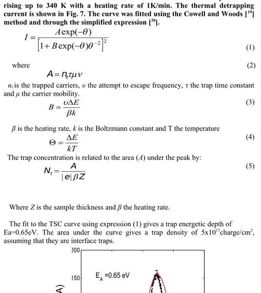
240 K. Then we measure the short-circuited current while the temperature is rising up to 340 K with a heating rate of 1K/min. The thermal detrapping
current is shown in Fig. 7. The curve was fitted using the Cowell and Woods [19]
method and through the simplified expression [20].
2
2)
exp(
1
)
exp(
B
A
I
(1) whereA n
tmn
(2)nt is the trapped carriers, υ the attempt to escape frequency, τ the trap time constant
and μ the carrier mobility.
k E B (3)
β is the heating rate, k is the Boltzmann constant and T the temperature
kT E
(4)
The trap concentration is related to the area (A) under the peak by:
Nt A
|e|Z
(5)
Where Z is the sample thickness and β the heating rate.
The fit to the TSC curve using expression (1) gives a trap energetic depth of Ea=0.65eV. The area under the curve gives a trap density of 5x10¹⁷charge/cm2, assuming that they are interface traps.
Fig. 7. Thermally stimulated current measured under short-circuited condition. The peak area provides a trap concentration of 2000 5x10¹⁷ 250charge/cm3002 with activation energy of 0.65eV. 350 400
50 100 150 200 Temperature (K) C u rr e n t ( p A ) EA =0.65 eV 0 1 2 3 4 5 6 -5 0 5 10 15 20x 10 -9
Temperature (K)
C
ur
re
nt
(
pA
)
s70321c3d3 0 1 2 3 4 5 6 -5 0 5 10 15 20x 10 -9Temperature (K)
C
ur
re
nt
(
pA
)
s70321c3d35 Conclusion
In summary, we have determined density and energetic location of electron traps in polymer-oxide memories employing a thermal stimulated current method. The trapped charges establish an electric field across the oxide. When the internal field reaches a critical value, soft-breakdown occurs, yielding an active memory diode. This controlled soft-breakdown mechanism allows for better tuning of the memory characteristics in respect oxide only memories.
Acknowledgement. We gratefully acknowledge the financial support received from the Dutch Polymer Institute (DPI), project n.º 703, from Fundação para Ciência e Tecnologia (FCT) through the research Unit, Center of Electronics Optoelectronics and Telecommunications (CEOT), REEQ/601/EEI/2005 and the POCI 2010, FEDER.
1 Kukreja, L.M, Das, A.K., Misra, P.: Bull. Mater. Sci. 32, 247–252 (2009) 2 Akinaga, H., Shima, H.: Proceedings of the IEEE 98, 2237–2251 (2010) 3 Sawa, A.: Materials Today 11, 28–36 (2008)
4 Robertson, J.: Eur. Phys. J. Appl. Phys. 28, 265–291 (2004)
5 Specht, M., Reisinger, H., Hofmann, F., Schulz, T., Landgraf, E., Luyken, R.J., Rösner, W., Grieb, M., Risch, L.: Solid-State Electronics49, 716–720 (2005)
6 Hickmott, T.W.: J. Appl. Phys. 33, 2669–2682 (1962)
7 Srivastava,S.K., Bhattacharyya, R.: Thin Solid Films 9, 357–361 (1972 )
8 Bory,B.F., Meskers, S.C.J., Janssen, R.A.J., Gomes, H.L., Leeuw, D.M. De: Appl. Phys. Lett. 97, 222106 (2010) 9 Shatzkes, M., Av–Ron, M., Anderson, R.M.: J. Appl. Phys. 45, 2065–2077 (1974)
10 Hickmott, T.W.: J. Appl. Phys. 88, 2805–2812 (2000)
11 Liu, D., Robertson, J.: Microelectronic Engineering 86, 1668–1671 (2009) 12 Heuer, A.H.: J. of the European Ceramic Society 28, 1495–1507 (2008)
13 Li, Y.T., Long, S.B., Lv, H.B., Liu, Q., Wang, Y., Zhang, S., Lian, W.T., Wang, M., Zhang, K.W., Xie, H.W., Liu, S., Liu, M.: Nanotechnology 22, 254028–254032 (2011)
14 Andreasson, B.P., Janousch, M., Staub, U., Meijer, G.I., Ramar, A., Krbanjevic, J., Schaeublin, R.: J. of Phys. 190, 012074 (2009) 15 Oxley, D.P.: Electrocomponent Sci. Technol. 3, 217–224 (1977)
16 Mills, C.A., Taylor, D.M., Riul, A.Jr., Lee, A.P.: J. Appl. Phys. 91, 5182–5189 (2002) 17 De Nijs, J.M.M., Balk, P.: Microelectronic Engineering22, 123–126 (1993) 18 Hickmott, T.W.: J. Appl. Phys. 88, 2805–2812 (2000)
19 Cowell, T.A.T., Woods, J.: Br. J. Appl. Phys. 18, 1045–1051 (1967) 20 Meier, M., Schwoerer, M.: J. Appl. Phys. 84, 87–92 (1998)