*e-mail: [email protected]
1. Introduction
Nanostructured surfaces have found growing applications in different areas like optoelectronics, physical chemistry, optics and photonics, photovoltaic cells, photocatalysis, cellular biology, microbiology, biochemistry, electrical and electronic engineering, mechanical and aerospace engineering, among other ields. Based-plasma processes are correlated with the nanotechnology development. Among these processes we can highlight the magnetron sputtering, for deposition of nanostructured films1. In magnetron
sputtering systems, the energy delivered to the ilm comes from external heating, chemical reactions on the surface and collisions with electrons, ions, radicals and neutral atoms2,3.
The total amount of energy transferred to the ilm is the difference between the total inlet energy and the dissipated energy. It promotes the nucleation and growth of the ilm and affects their stoichiometry and adhesion to substrate.
For magnetron sputtering systems, the energy delivered to the substrate during the ilm deposition depends of several process variables, such as: power source (e.g. DC, pulsed magnetron sputtering (PMS), high power pulsed magnetron sputtering (HIPIMS) and modulated pulsed power magnetron sputtering (MPP))2-5; the anode-cathode
geometry6,7; the magnetic ield coniguration8-10, and the
substrate bias11,12. These variables are not independent and
it is dificult to do a correlation between them2,13. The ion
bombardment control has received great attention due to the possibility of change the ilm structure in micro and nanometer scales. Moreover it can improve the adherence of the ilms to the substrate and change the crystallographic texture and roughness of the ilms14. Nevertheless, few
studies have been done in relation to the control of the pulsed substrate bias15-17. Due the interest in Ti alloys
films, this paper investigates the effect of pulsed bias voltage (Vbias) in comparison with DC bias on crystallinity and roughness of Ti6Al4V-N ilms obtained by reactive deposition, using a grid assisted magnetron sputtering system. Ti6Al4V alloy was chosen due to your resistance to wear and fatigue, weathering and corrosion. It has been applied in aerospace and medicine with a good combination of mechanical, chemical, physical and biocompatibility18,19.
The morphological properties of these ilms were analyzed by X-Ray diffraction (XRD), Energy Dispersive X-ray Fluorescence Spectrometer, (EDX) and Atomic Force Microscopy (AFM).
2. Experimental Details
The depositions were carried out in a stainless steel chamber with 28.0 cm in diameter and a height of 24.0 cm. The chamber walls are grounded. The target-substrate distance was ixed in 7.0 cm, being the target a planar disk Ti6Al4V (99.6% purity, 100mm diameter). Between the target and the substrate there is a grounded AISI 304 stainless steel grid that acts as the discharge anode, making plasma maintenance easier6. The cathode (12.4 cm in diameter) is
mounted on an unbalanced magnetron. A mask shield system allowed the introduction of six samples for each deposition cycle. While a deposition was performed over one sample, another ive samples were kept protected by a mask and so on. All ilms were deposited on substrates of AISI 304 stainless steel during 30 minutes. The magnetron discharge voltage was set at 440 V resulting in a current around 1.0 A. The substrate temperature was set in 300°C and it was controlled by a heating system consisting of four 250 W halogen lamps and a temperature control system. The pressure in the chamber was measured by two Pirani gauges
Pulsed Bias Effect on Crystallinity and Nano-Roughness of Ti6Al4V-N Films
Deposited by Grid Assisted Magnetron Sputtering System
Joel Stryhalskia,b*, Luis César Fontanaa, Marcos Fernando Odorczyka, Juliano Sadi Scholtza,
Julio César Sagása,c, Abel André Candido Reccoa
aPhysics Department, santa Catarina state University – DEsC, Joinville, sC, brazil bPhysics Department, Federal institute of santa Catarina – iFsC, Jaraguá do sul, sC, brazil
cCatólica de santa Catarina, Joinville, sC, brazil
Received: February 7, 2014; Revised: September 14, 2014
This paper reports the effect of pulsed bias in comparison with DC bias on reactive deposition of Ti6Al4V-N ilms, obtained by Grid Assisted Magnetron Sputtering. The results obtained by X-Ray diffraction (XRD), Energy Dispersive X-ray Fluorescence Spectrometer (EDX) and Atomic Force Microscopy (AFM) show that bias condition affects the crystalline texture and change the roughness and morphology of the ilms. The DC bias favors the ilm crystallinity, however the pulsed bias produces smoother ilms.
(in the range between 760 Torr and 10–3 Torr) and a Penning
gauge (in the range between 10–3 Torr and 10–7 Torr). Table 1
shows the deposition parameters.
The gases mass low rate (Ar 99.99% and N2 99.99%)
were measured by mass low controllers. The voltage source used to generate the plasma was a switching power supply, with current control from 0.0A to 2.0A and voltage up to –1000V related to the ground. The samples were electrically isolated from the chamber walls (grounded), enabling the negative bias of the substrate with respect to the ground, as shown in Figure 1. The bias power supply used in this work allowed us change the pulsed bias between 0 and –300V (peak to peak at 1.0 kHz) and the adjustment of duty cycle or “time on”/“time off” periods.
During the “time off” the substrate was under loating potential. The ratio “time on”/“period” is called “duty cycle”. The depositions were carried out using 20% duty cycle as well DC bias. It was used a low “duty cycle” value (20%) just to compare with DC mode, where the ions bombardment is continuum.
The samples were characterized by AFM Nanosurf Nanite B S200 model at contact mode for surface morphology and roughness characterization in nanometer scale. The formation of crystalline phases was examined by XRD. The thickness was measured by an indirect method using Energy Dispersive x-ray spectrometer (EDX) Shimadzu EDX-720.
3. Results and Discussion
Three values of bias voltage were studied: –100V, –200V and –300V at 1.0kHz frequency and 20% duty cycle. For comparison it was used DC bias. The Figure 2 shows the voltage and current waveforms for duty cycle of 20%. At bottom of this igure it is shown the voltage (in V) and on top the current (in mA). It is possible to see that the bias current drops toward zero when the voltage is switched off. When the current reaches zero, the sample is in loating potential. It was used the traditional method of the hysteresis curve to determine the proportion of N2/Ar low (reactive and inert gas low to the chamber) for stoichiometric ilm deposition with high deposition rate20. The optimal point for
stoichiometric Ti6Al4V-N ilm deposition, corresponding to 2.2 sccm and 2.6 sccm for N2 and Ar low respectively (N2/Ar = 0.85).
The average current in pulsed mode is lower than in DC mode, as can be seen in Table 2. However the peak current density (at peak pulse voltage) is signiicantly higher than DC bias current. This means that peak power delivered to substrate is higher in pulsed mode, although the average power is higher in DC mode.
Average ilm thickness of the samples was 0.4±0.2μm for all samples. The exception was the ilm deposited at
Vbias = –300V in DC mode, in which we observed a thinner ilm with thickness approximately 0.05mm. At this voltage the ions acquire suficient energy to produce considerable re-sputtering of ad-atoms during the deposition, resulting in a thinner ilm.
X-ray diffraction spectra (Figure 3) show three peaks of high intensity at 2θ angles of 43.6°, 50.8°, 74.6°, relative to the AISI 304 stainless steel substrate. The peaks relative to
Ti6Al4V-N ilms appears at 2θ angles of 37,2°, 42,8°, 62,1° indicating the formation of cristal planes (111), (200) and (220) of TiN respectively20. At bias voltage of –100V and
–200V, it is possible to see more intense (111) and (200) peaks for DC bias mode than for pulsed mode. However at –300V bias it is possible to observe more intense peaks (111), (200) and (220) for pulsed mode (20% duty cycle, 1kHz). The high power delivered to the substrate due
Table 1. Deposition parameters.
Ar mass low rate 2.64 sccm
N2 mass low rate 2.20 sccm
Target voltage –440 V (DC)
Duty Cycle 20%
Target current 1.0 A
Deposition pressure 3.5 mTorr (0.47Pa)
Substrate temperature 300 ± 10 °C
Deposition time 30 min
Vbias (DC and pulsed at 1.0kHz) –100V, –200V and –300V
Figure 1. Overview of the experimental setup, showing the arrangement of the target, the substrate, the grid and the electrical connections.
Figure 2. Waveform for voltage (V) on bottom and current on top
bombardment at –300V DC promotes resputtering and probable amorphization of the ilm. On the other hand, for –300V bias in pulsed mode also occurs bombardment by energetic ions, but the intermittent ion bombardment (20% on) is suficient to allow the adatoms diffusion and time (80% off) for nucleation and growing of the grains on substrate surface.
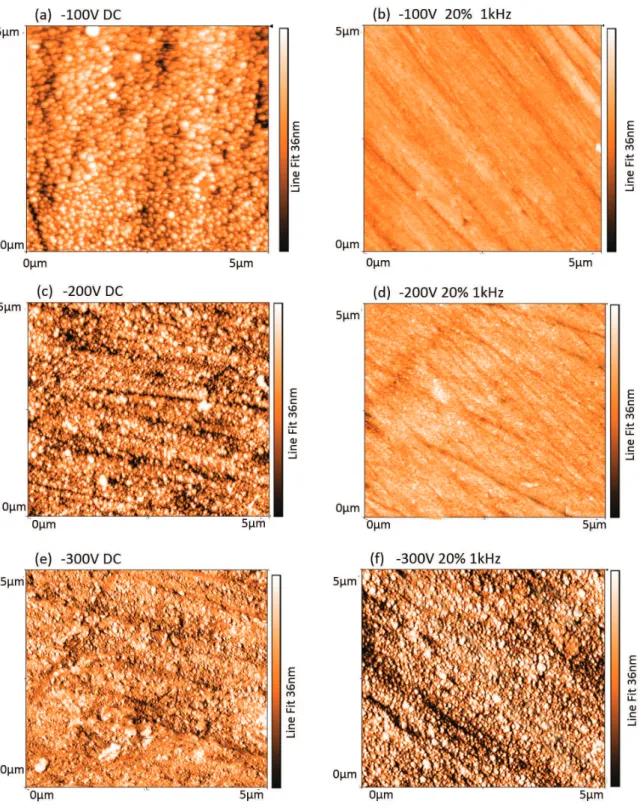
The topographies of ilm surfaces are shown in Figure 4 and were obtained with atomic force microscopy – AFM. Pictures have dimensions of 5mm × 5mm. The roughness values are shown in Table 3. The roughness is higher for
ilms deposited under DC bias for –100V and –200V and for –300V pulsed bias. Films with higher roughness have more intense peaks (111), (200) and (220) of TiN in XRD pattern, that are the samples corresponding to DC bias –100V and –200V and pulsed bias –300V at 1kHz and 20% duty cycle. The smoother ilms are corresponding to pulsed bias –100V and –200V and less intense peaks in XRD spectra. It indicates that the growing of crystalline ilms results in rougher surfaces. This can be attributed to formation of crystalline texture on the surface due a preferential growing direction of the grains.
Table 3. Roughness Ra of ilms.
Bias Voltage (V) –100 –200 –300
Bias mode DC 20%, 1kHz DC 20%, 1kHz DC 20%, 1kHz
Routhness (Ra) 5.3nm 1.9nm 5.0nm 2.3nm 4.1nm 6.5nm
Figure 3. XRD spectra (a) –100VDC × –100V, 20%, 1kHz, (b) –200VDC × –200V, 20% 1kHz, (c) –300VDC × –300V, 20% 1kHz. Table 2. Substrate current bias obtained for different voltages and bias modes.
Bias mode –100VDC –100V, 20%,
1kHz
–200VDC –200V, 20%,
1kHz
–300VDC –300V, 20%,
1kHz
Current density (µA/cm2)
Peak
30 85 70 120 140 170
Average 10 40 70
Power density (mWatt/cm2)
Peak
3.0 8.5 14.0 24.0 42.0 51.0
Figure 4. AFM images for DC and pulsed bias, images size are 5 mm × 5 mm. (a) –100V DC; (b) –100V pulsed; (c) –200V DC; (d) –200V pulsed; (e) –300V DC and (f) –300V pulsed.
4. Conclusion
The effects of pulsed and DC substrate bias on the surface morphology and cristalinity of Ti6Al4V-N ilms deposited by Grid Assisted Magnetron Sputtering were investigated. Pulsed bias causes changes in crystallinity and nano-roughness. Different combinations of bias values
(voltage, frequency and duty cycle) can provide appropriate energy delivery and time for adatoms diffusion in the growing ilm.
ilms induces rougher surfaces due to preferential directions of nano-crystal growth.
The choice of frequency, duty cycle and voltage can be used to grow ilms with the same crystal planes observed with DC bias, but with smoother surfaces. For DC mode bias, signiicant changes were not observed in ilm roughness; however, amorphous ilms can be produced as
well as there-sputtering of adatoms from the substrate, when it is biased with high voltage (for example Vbias = –300V).
Acknowledgements
The authors thank the Fundo de Apoio à Manutenção e ao Desenvolvimento da Educação Superior - FUMDES of Santa Catarina State for inancial support.
References
1. Ostrikov K, Cvelbar OU and Murphy AB. Plasma nanoscience:
setting directions, tackling grand challenges. Journal of
Physics D: applied Physics. 2011; 44(17). http://dx.doi.
org/10.1088/0022-3727/44/17/174001.
2. Kersten H, Deutsch H, Steffen H, Kroesen GMW and Hippler
R. The energy balance at substrate surfaces during plasma processing. Vacuum. 2001; 63(3):385-431. http://dx.doi. org/10.1016/S0042-207X(01)00350-5.
3. Mishra A, Kelly PJ and Bradley JW. The 2D plasma potential
distribution in a HiPIMS discharge. Journal of Optoelectronics
and advanced Materials. 2009; 44:1101-1107.
4. Sarakinos K, Alami J and Konstantinidis S. High power pulsed magnetron sputtering: A review on scientific and engineering state of the art. surface and Coatings Technology. 2010; 204(11):1661-1684. http://dx.doi.org/10.1016/j. surfcoat.2009.11.013.
5. Safi I. The properties of reactively-sputtered, stoichiometry-controlled and optimum-conductivity transparent indium
oxide films as a function of their titanium, aluminium and zinc
content; comparison with the use of thin as a dopant. surface
and Coatings Technology. 2000; 127(2-3):203-219. http://
dx.doi.org/10.1016/S0257-8972(00)00566-1.
6. Fontana LC and Muzart JLR. Characteristics of triode
magnetron sputtering: the morphology of deposited titanium films. surface and Coatings Technology. 1998; 107(1):24-30. http://dx.doi.org/10.1016/S0257-8972(98)00576-3.
7. Nam KH, Jung MJ, Han JG, Kopte T, Hartung U and Peters C.
Synthesis of high-density MgO films by a novel magnetron sputtering system. Vacuum. 2004; 75(1):1-6.
8. Berg S and Nyberg T. Fundamental understanding and
modelling of reactive sputtering processes. Thin solid
Films. 2005; 476(2):215-230. http://dx.doi.org/10.1016/j.
tsf.2004.10.051.
9. Shidoji E and Toshiaki T. Magnetron plasma structure with strong magnetic field. Thin solid Films. 2003; 442(1-2):27-31. http://dx.doi.org/10.1016/S0040-6090(03)00933-7.
10. Sagás J, Fontana L and Maciel H. Influence of electromagnetic confinement on the characteristics of a triode magnetron sputtering system. Vacuum. 2011; 85(6):705-710. http://dx.doi. org/10.1016/j.vacuum.2010.11.002.
11. Lee J-W, Kuo Y-C, Wang C-J, Chang L-C and Liu K-T. Effects
of substrate bias frequencies on the characteristics of chromium
nitride coatings deposited by pulsed DC reactive magnetron sputtering. surface and Coatings Technology. 2008; 203(5-7):721-725. http://dx.doi.org/10.1016/j.surfcoat.2008.08.039.
12. Wei Y and Gong C. Effects of pulsed bias duty ratio
on microstructure and mechanical properties of TiN/ TiAlN multilayer coatings. applied surface science. 2011; 257(17):7881-7886. http://dx.doi.org/10.1016/j. apsusc.2011.04.066.
13. Han J. Recent progress in thin film processing by magnetron sputtering with plasma diagnostics. Journal of Physics D:
applied Physics. 2009; 42(4).
14. Lin J, Moore JJ, Mishra B, Pinkas M, Sproul WD and Rees JA. Effects of substrate bias frequencies on characteristics of
chromium nitride coatings deposited by pulsed DC reactive magnetron spurrering. surface and Coatings Technology. 2008; 202(8):1418-1436. http://dx.doi.org/10.1016/j. surfcoat.2007.06.068.
15. Griepentrong M, Mackrodt B, Mark G and Linz T. Properties
of TiN hard coatings prepared by unbalanced magnetron sputtering and cathodic are deposition using a unipolar and bipolar pulsed bias voltage. surface & Coatings Technology. 1995; 74:326-332.
16. Cooke K, Hamsphire J, Southall W and Teer D. The industrial application of pulsed DC bias power supplies in closed field unbalanced magnetron sputter ion plating. surface and
Coatings Technology. 2004; 177-178:789-794.
17. Kelly PJ, Hall R, O’Brien J, Bradley JW, Roche G and Arnell RD. Substrate effects during mid-frequency pulsed DC biasing.
surface & Coatings Technology. 2001; 142-144:635-641.
18. Jinlong L, Mingren S, Xinxin M, Feng H and Qunji X. Influence of annealing on mechanics behaviors of oxygen-implanted layer on Ti6Al4V by plasma-based ion implantation. surface
and Coatings Technology. 2013; 228(1):S224-S227. http://
dx.doi.org/10.1016/j.surfcoat.2012.06.001.
19. Zhang CZ, Li YS, Tang Y, Yang L, Zhang L, Sun Y, et al. Nanocrystalline diamond thin films grown on Ti6Al4V alloy. Thin solid Films. 2013; 527:59-64. http://dx.doi.org/10.1016/j. tsf.2012.12.014.