Bruno Miguel Rocha Martins
BsC
Electrochemical Supercapacitors Of Conductive
Polymers And Their Composites
Dissertação Para Obtenção Do Grau De Mestre Em
Bioorgânica
Orientadora: M. Fátima Montemor, Prof. Dra., IST-UL
Co-orientadora: M. Margarida Cardoso, Prof. Dra., FCT-UNL
Júri:
Presidente: Prof. Doutora Paula Cristina de Sério Branco
Arguente: Prof. Doutora Raquel Alexandra Galamba Duarte
Vogal: Prof. Doutora Maria de Fátima Grilo da Costa Montemor
ii
E
LECTROCHEMICALS
UPERCAPACITORS OFC
ONDUCTIVEP
OLYMERS ANDT
HEIRC
OMPOSITESCopyright Disclaimer
The Faculdade de Ciências e Tecnologia, Universidade Nova de Lisboa and the Grupo
de Estudos de Corrosão e Efeitos Ambientais have the, perpetual and geographically
unrestricted, right to store and publish this dissertation in paper print or digital examplaries, or
by any other method known or still to be invented, and to divulge it through scientific databases
and approve its copy and distribution with educational or research purposes, not commercial, as
long as the credit is attributed to its author and editor.
E
LECTROCHEMICALS
UPERCAPACITORS OFC
ONDUCTIVEP
OLYMERS ANDT
HEIRC
OMPOSITESDeclaração de Direitos de Cópia
A Faculdade de Ciências e Tecnologia, a Universidade Nova de Lisboa e o Grupo de
Estudos de Corrosão e Efeitos Ambientais têm o direito, perpétuo e sem limites geográficos, de
arquivar e publicar esta dissertação através de exemplares impressos reproduzidos em papel ou
de forma digital, ou por qualquer outro meio conhecido ou que venha a ser inventado, e de a
divulgar através de repositórios científicos e de admitir a sua cópia e distribuição com
objectivos educacionais ou de investigação, não comerciais, desde que seja dado crédito ao
iv
Acknowledgements
Regarding the work done on in this thesis I would like to acknowledge both my
supervisors, Prof. M. Fátima Montemor and Prof. Margarida Cardoso for all the patience,
support and the chance of doing this. I also want to acknowledge my family for their continual
support and everybody in the GECEA group for all they have taught me.
Finally I would like to thank the coordinator of the Bioorganic Chemistry Masters in the
New University of Lisbon (UNL) for the priceless chance and support she gave throughout my
vi
Resumo
Neste trabalho experimental foram desenvolvidos supercondensadores de polianilina
(PANI) suportada num substrato de aço inoxidável AISI304L e formada através de uma reação
de auto-organização de polimerização por oxidação química em meio aquoso. O efeito de
diversas variáveis na formação dos filmes e partículas depositadas, na sua morfologia e na
capacidade específica destes, foi estudado. As variáveis estudadas foram: a espécie oxidante; as
concentrações do oxidante, anilina, ácido sulfúrico e ácido fosfórico; e o efeito da adição de
alguns óxidos metálicos. As melhores condições reaccionais, em relação às capacidades
especificas electroquímicas foram: 4.15x101F.g-1, para 1x10⁻²M de K2S2O8; 7.41x101F.g-1 para
1x10⁻²M de anilina; 3.41x10²F.g-1 para 5M de ácido fosfórico; 4.44x10²F.g-1 para 5x10⁻¹M de ácido sulfúrico; 2.10x10²F.g-1 para 34 horas de reação; e o melhor óxido metálico testado foi o dióxido de manganês (IV) com 1.60x10²F.g-1.
Palavras-chave: polianilina, aço inoxidável AISI304L, supercondensadores,
auto-organização
Abstract
In this experimental work, polyaniline (PANI) supercapacitors, supported on AISI304L
stainless steel, were developed by self-assembly chemical oxidative polymerization in aqueous
medium. The effect of several variables on the deposited films and particles, their morphologies
and specific capacitances was studied. The variables studied were: oxidant species; oxidant,
aniline, sulfuric acid and phosphoric acid concentrations; and effect of the addition of metallic
oxides. The best reaction conditions, regarding the obtained specific capacitances were:
4.15x101F.g-1, for 1x10⁻²M of K2S2O8; 7.41x101F.g-1 for 1x10⁻²M of aniline; 3.41x10²F.g-1 for
5M of phosphoric acid; 4.44x10²F.g-1 for 5x10⁻¹M of sulphuric acid; 2.10x10²F.g-1 for 34 hours of reaction; and the best metallic oxide tested was manganese (IV) dioxide with 1.60x10²F.g-1.
viii
Table of Contents
Copyright Disclaimer ... ii
Declaração de Direitos de Cópia ... ii
Acknowledgements ... iv
Resumo ... vi
Abstract ... vi
Table of Figures ... x
Table of Tables ... xiv
Abbreviations List ... xvi
1. Introduction ... 1
2. Materials ... 2
2.1. Polyaniline as a Supercapacitor ... 2
2.2. Polyaniline Synthesis by Chemical Oxidation ... 4
2.3. Electrical Conductivity in Polyaniline ... 5
2.4. Semiconductors ... 6
2.4.1. Doping ... 8
2.4.2. Properties of Organic Semiconductors ... 8
3. Techniques ... 8
3.1. Scanning Electron Microscopy ... 8
3.1.1. Raman Microscopy ... 9
4. Materials and Methods ... 13
5. Results and Discussion ... 17
5.1. Reaction Set 1 – Substrate Effect ... 18
5.2. Reaction Set 2 – Oxidant Species ... 20
5.3. Reaction Set 3 – Oxidant Concentration ... 25
5.4. Reaction Set 4 – Aniline Concentration ... 29
5.5. Reaction Set 5 – Phosphoric Acid Concentration ... 31
5.6. Reaction Set 6 – Sulfuric Acid Concentration ... 35
ix
5.8. Reaction Set 8 – Metallic Oxides Addition ... 44
6. Conclusions ... 47
7. Future Work ... 48
x
Table of Figures
Figure 1 – Different polyaniline oxidation states and protonation levels29. ... 3 Figure 2 – Initiation mechanism of aniline chemical oxidative polymerization. ... 4 Figure 3 – From the top-down: emeraldine base before and after partial (50%) protonation, and corresponding bipolaron and polaron27. ... 6
Figure 4 – Examples of different structures usually detected by Raman spectra of PANI synthesized by chemical oxidative polymerization in aqueous medium. ... 12
Figure 5 - Horiba LabRAM HR Evolution (adapted from ref. 49) ... 16 Figure 6 – Experimental setup used in electrochemical tests (left) and detail of the electrochemical cell (right). ... 17
Figure 8 – Raman spectra of the surface of the AISI304L stainless steel samples exposed to the reactions of set 2. ... 21
Figure 9 – Photos taken with the Raman microscope (50x magnification) of the surface of the samples from the reactions with K2S2O8 (left) and NaClO (right). ... 22
Figure 10 – Cyclic voltammogram of sample from reaction set 1 done using NaClO as the oxidant species. The potential range is between -400 and 300mV, electrolyte H3PO4 solution
at pH 2 and potential sweep speed of 50mV.s-1. ... 22 Figure 11 - Cyclic voltammogram of sample from reaction set 1 done using K2S2O8 as
the oxidant species. The potential range is between 200-500mV, electrolyte H3PO4 solution at
pH 2 and potential sweep speed of 50mV.s-1. ... 23 Figure 12 – Charge-discharge cycle of sample from set 1 with NaClO using 10A.g-1 current. The potential range is between -400 and 300mV and the electrolyte H3PO4 solution at
pH 2. ... 24
Figure 13 - Charge-discharge cycle of sample from set 1 with K2S2O8 using 10A.g-1
current. The potential range range is between 200 and 500mV and the electrolyte H3PO4
solution at pH 2. ... 24
Figure 14 - SEM of the top (left) and cross-section (right) of the sample of reaction set 2
done using NaClO. ... 25
Figure 15 - SEM of the top (left) and cross-section (right) of the sample of reaction set 2
done using K2S2O8. ... 25
Figure 16 - Raman spectra of the surface of the AISI304L stainless steel samples
exposed to the reactions of set 3. ... 26
Figure 17 - Photos taken with the Raman microscope (50x magnification) of the surface
of the samples from the reactions with 1x10⁻²M (left) and 5x10⁻²M of K2S2O8. ... 26
Figure 18 - Photos taken with the Raman microscope (50x magnification) of the surface
xi Figure 19 – SEM of the top (left) and cross-section (right) of the sample of reaction set 3 done using 1x10⁻²M of K2S2O8. ... 27
Figure 20 - SEM of the top (left) and cross-section (right) of the sample of reaction set 3
done using 1x10⁻¹M of K2S2O8. ... 28
Figure 21 - SEM of the top (left) and cross-section (right) of the sample of reaction set 3
done using 2x10⁻¹M of K2S2O8. ... 28
Figure 22 – Raman spectra of the surface of the AISI304L stainless steel samples exposed to the reactions of set 4. ... 29
Figure 23 - Photos taken with the Raman microscope (50x magnification) of the surface
of the samples from the reactions with 1x10⁻²M (left) and 1M of aniline. ... 30 Figure 24 - SEM of the top (left) and cross-section (right) of the sample of reaction set 4
done using 1x10⁻²M of Aniline. ... 30 Figure 25 - SEM of the top (left) and cross-section (right) of the sample of reaction set 4
done using 1M of Aniline... 31
Figure 26 - Raman spectra of the surface of the AISI304L stainless steel samples
exposed to the reactions of set 5. ... 32
Figure 27 - Photos taken with the Raman microscope (50x magnification) of the surface
of the samples from the reactions with 5x10⁻⁴M (left) and 5x10⁻³M (right) of H3PO4. ... 32
Figure 28 - Photos taken with the Raman microscope (50x magnification) of the surface
of the samples from the reactions with 5x10⁻¹M (left) and 5M (right) of H3PO4. ... 33
Figure 29 - SEM of the top (left) and cross-section (right) of the sample of reaction set 5
done using 5x10⁻⁴M of H3PO4. ... 33
Figure 30 - SEM of the top (left) and cross-section (right) of the sample of reaction set 5
done using 5x10⁻³M of H3PO4. ... 34
Figure 31 - SEM of the top (left) and cross-section (right) of the sample of reaction set 5
done using 5x10⁻¹M of H3PO4. ... 34
Figure 32 - SEM of the top (left) and cross-section (right) of the sample of reaction set 5
done using 5M of H3PO4. ... 34
Figure 33 - Raman spectra of the surface of the AISI304L stainless steel samples
exposed to the reactions of set 6. ... 36
Figure 34 - Photos taken with the Raman microscope (50x magnification) of the surface
of the samples from the reactions with 5x10⁻⁴M (left) and 5x10⁻³M (right) of H2SO4. ... 36
Figure 35 - Photos taken with the Raman microscope (50x magnification) of the surface
of the samples from the reactions with 5x10⁻¹M (left) and 5M (right) of H2SO4. ... 37
Figure 37 - SEM of the top (left) and cross-section (right) of the sample of reaction set 6
xii Figure 38 - SEM of the top (left) and cross-section (right) of the sample of reaction set 6
done using 5x10⁻³M of H2SO4. ... 38
Figure 39 - SEM of the top (left) of the sample of reaction set 6 done using 5x10⁻¹M of H2SO4. ... 38
Figure 40 - SEM of the top (left) and cross-section (right) of the sample of reaction set 6
done using 5M of H2SO4. ... 38
Figure 41 - Raman spectra of the surface of the AISI304L stainless steel samples
exposed to the reactions of set 7. ... 40
Figure 42 - Photos taken with the Raman microscope (50x magnification) of the surface
of the samples from the reactions done during 2 hours (left) and 4 hours (right). ... 40
Figure 43 - Photos taken with the Raman microscope (50x magnification) of the surface
of the samples from the reactions done during 16 hours (left) and 34 hours (right). ... 41
Figure 44 - Photos taken with the Raman microscope (50x magnification) of the surface
of the samples from the reactions done during 48 hours. ... 41
Figure 46 - SEM of the top (left) and cross-section (right) of the sample of reaction set 7
done in 2 hours. ... 42
Figure 47 - SEM of the top (left) and cross-section (right) of the sample of reaction set 7
done in 4 hours. ... 42
Figure 48 - SEM of the top (left) and cross-section (right) of the sample of reaction set 7
done in 16 hours. ... 42
Figure 49 - SEM of the top (left) and cross-section (right) of the sample of reaction set 7
done in 34 hours. ... 43
Figure 50 - SEM of the top (left) and cross-section (right) of the sample of reaction set 7
done in 48 hours. ... 43
Figure 51 - Raman spectra of the surface of the AISI304L stainless steel samples
exposed to the reactions of set 8 and of the metallic oxides used. ... 44
Figure 52 - Photos taken with the Raman microscope (50x magnification) of the surface
of the samples from the reactions done using ZnO (left) and MnO2 (right). ... 45
Figure 55 - SEM of the top (left) and cross-section (right) of the sample of reaction set 8
done with ZnO. ... 46
Figure 56 - SEM of the top (left) and cross-section (right) of the sample of reaction set 8
xiv
Table of Tables
Table 1 – Raman peak wavelengths taken from the literature44, 45, 46 and 47, using different exposure times, accumulations and laser intensities from those used in this work. Legend: o.p. –
out-of-plane; i.p. – in-plane; ~ - bond between single and double. ... 11
Table 2 – Activated carbon substrates used. ... 13
Table 3 – AISI304L stainless steel composition ... 13
Table 4 – Reaction set 1 tested variable: substrate effect. ... 14
Table 5 - Reaction set 2 tested variable: oxidant species effect. ... 14
Table 6 - Reaction set 3 tested variable: oxidant (K2S2O8) concentration. ... 14
Table 7 - Reaction set 4 tested variable: aniline concentration. ... 15
Table 8 - Reaction set 5 tested variable: H3PO4 concentration. ... 15
Table 9 - Reaction set 6 tested variable: H2SO4 concentration. ... 15
Table 10 - Reaction set 7 tested variable: reaction time. ... 16
Table 11 - Reaction set 8 tested variable: metallic oxide particle addition. ... 16
Table 12 – Mass and conductivity of the PANI self-assembled over the substrates tested. ... 19
Table 13 – Mass of self-assembled deposit over the AISI304L stainless steel substrate per unit of sample area. ... 20
Table 14 - Mass of deposit self-assembled over the AISI304L stainless steel substrate per unit of sample area. ... 25
Table 15 – Potential intervals and specific capacitances of the deposits formed on the surface of the AISI304L stainless steel samples exposed to the reactions of set 3. ... 27
Table 16 - Mass of deposit self-assembled over the AISI304L stainless steel substrate per unit of sample area. ... 29
Table 17 - Potential intervals and specific capacitances of the deposits formed on the surface of the AISI304L stainless steel samples exposed to the reactions of set 4. ... 30
Table 18 - Mass of deposit self-assembled over the AISI304L stainless steel substrate per unit of sample area. ... 31
Table 19 - Potential intervals and specific capacitances of the deposits formed on the surface of the AISI304L stainless steel samples exposed to the reactions of set 5. ... 33
Table 20 - Mass of deposit self-assembled over the AISI304L stainless steel substrate per unit of sample area. ... 35
Table 21 - Potential intervals and specific capacitances of the deposits formed on the surface of the AISI304L stainless steel samples exposed to the reactions of set 6. ... 37
xv Table 23 - Potential intervals and specific capacitances of the deposits formed on the
surface of the AISI304L stainless steel samples exposed to the reactions of set 7. ... 41
Table 24 - Mass of deposit self-assembled over the AISI304L stainless steel substrate
per unit of sample area. ... 44
Table 25 - Potential intervals and specific capacitances of the deposits formed on the
xvi
Abbreviations List
µ - Charge mobility
σ– Electrical conductivity BG – Band Gap
CB – Conduction Band DMF - Dimethylformamide
DMSO - Dimethylsulfoxide
e– Electrical charge
EDLS - Electric Double Layer Supercapacitors
EF– Fermi Energy Level Potential
EIS – Electrochemical Impedance Spectroscopy ES – Electrochemical Supercapacitors
FS – Faradaic Supercapacitors
HOMO - Highest Occupied Molecular Orbital
K – Kelvin
LUMO - Lowest Unoccupied Molecular Orbital
n– Charge carriers density NMP - 1-methyl-2-pyrrolidinone
PANI – Polyaniline
PEDOT - Poly(3,4-ethylenedioxythiophene)
PCA – Principal Component Analysis Ppy - Polypyrrole
SCE – Saturated Calomel Electrode T – Temperature
1
1.
Introduction
Environmental issues, fossil fuel availability and economical pressures have brought up
urgency for clean, efficient and sustainable energy sources. With this, the need for new energy
conversion and storage technologies also increases. From these, the ones which have attracted
more attention in the last few years are fuel cells, batteries and electrochemical supercapacitors
(ES)1.
The source for the interest in ES is their high power density and output, and long
lifecycle. They fill the gap between dielectric capacitors and batteries or fuel cells, which have
high power output and high energy storage capacities. Despite the fact that the first
supercapacitor patent was submitted in 1957, the real interest for this technology was only
rekindled when the market of hybrid electric vehicles started to grow. This happened because
ES are able to provide high power outputs, which are necessary for acceleration, and to
accumulate some energy from the breaking process1.
With the development of this ES technology other possible applications were found,
such as power back-up elements for fuel cells and batteries when power disruptions occur, and
voltage stabilizers. In fact, the US Department of Energy has declared ES as energy systems of
the same importance of batteries and fuel-cells1.
The current disadvantages of this technology are their high price compared to batteries
and low energy density. The energy density is strongly dependent upon the electrode material
given that it is the most important element in an ES1. Thus the search for cheaper and better performing materials for electrodes in electrochemical supercapacitors is crucial in order to
achieve a broader range of possible applications and usage.
One of the main characteristics that is searched for in these materials is a high surface
area and porosity. This arises from the fact that the energy can be stored at this interface between the electrode’s electrically conductive material and the electrolyte. This can be treated like a conventional capacitor displaying an electrical double-layer according to the following
expression:
where is the capacitance, is the active suface of the supercapacitor electrode, is the
dielectric constant of the electrolyte and is the thickness of the double layer. From this
equation we can understand that the electrochemical supercapacitors are able to store large
2 its surface, when compared with conventional electrical double layer capacitors. Beyond these
surface phenomena, certain electrode materials can themselves suffer electrochemical reactions.
These different phenomena are at the source of the main ES classes, namely, electric double
layer supercapacitors (EDLS) and faradaic supercapacitors (FS). In EDLS the electrostatic
energy is stored at the electrode/electrolyte interface in an electrode-potential-dependent way.
At this interface, when a potential is applied, an accumulation or deficit of electric charges
occurs at the surface of the electrode which is counterbalanced by charged electrolyte ions1. The most commonly used material for this type of supercapacitor is carbon (e.g. graphite oxide2, carbon black3, graphene4, carbon nanotubes5 and others6). In FS or pseudocapacitors the main charge storage mechanism is different. By applying a potential to these electrode materials a fast
and reversible redox reaction occurs which causes a charge transfer between this and the
electrolyte, a faradaic process. These redox reactions also cause electrostatic energy storage by
electrolyte ions organization for charge counterbalancing (by electrosorption and ion
intercalation) a non-faradaic process. Some of the types of materials which display this
behaviour and have been studied for these applications are metallic oxides (e.g. MnO27, Co3O48,
Ti0.6Ru0.4O29, NiOx10, Ni(OH)211, V2O512, amongst others13) and conducting polymers (e.g.
polyaniline (PANI)14, polypyrrole (PPy)15, poly(3,4-ethylenedioxythiophene) (PEDOT)16, amongst others17).
2.
Materials
In the last decades, the state of the art shows an increase in the creation of composites with
materials that store energy by non-faradaic processes with those that do it with faradaic ones.
Some examples of this are graphene/vanadium oxide nanotubes18, graphene/PANI19, Fe3O4/graphene20, carbon nanotubes/polypyrrole21, amongst others.
PANI was the material chosen for this study given that it is known having a high
theoretical22 electrochemical specific capacitance of 2000F.g-1, low-cost monomer and an easy one-pot synthesis. ES electrodes of PANI14 have reached values of 609F.g-1, and PANI composites values of 1300F.g-1 with stainless steel23 and 1486F.g-1 with carbon black24.
2.1.
Polyaniline as a Supercapacitor
Polyaniline was first discovered in 1835 as ―aniline black‖, a general expression used to refer to any product resulting from aniline oxidation25. It is one of the most studied conducting polymers given its environmental stability, easy synthesis (even in mild conditions), low cost of
the monomer, and its useful and unique electrical, electrochemical and electrochromic
3 shielding, non-linear optics, digital memory devices, artificial muscles, electrochromic displays,
fuel cells, solar cells, diodes, organic or polymer light emitting diodes, p-n heterojunctions,
amongst others27. However, despite all these and its easy processability, the fact that it decomposes at temperatures below those of softening or melting, makes its melt processing
impossible26.
The interest of PANI as a supercapacitor comes from the fact that the electrochemical
redox processes that occur in its polymeric chains are basically a sequential production of Lewis
bases that generate a multiply charged structure. The capacitance that arises from these is
significant and can be regarded as redox pseudocapacitance. Given that these redox processes
do not cause significant structural changes, and the metal-like behaviour of the polymer can
formally describe this capacitance as being of the double-layer kind. In fact, the reversibility of
these redox phenomena and the continuous range of oxidation potentials that occur with a
growing applied pontential are behind the symmetrical cyclic voltammograms and the
potential-sweep dependent response currents observed. Polyaniline can also be regarded as an organic
semiconductor28.
Figure 1 – Different polyaniline oxidation states and protonation levels29.
Polyaniline can be synthesized by chemical, electrochemical, photochemical,
4 oxidative polymerisation of aniline, either in organic or aqueous solvents, using oxidizing
agents such as, (NH4)2S2O830, FeCl3, KIO326, NaClO, K2Cr2O726, H2O2, enzymes, amongst
others. The difficulties behind chemical synthesis are the impact of the following variables on
its morphology and properties26: pH31, aniline/oxidant ratio, cationic species present in solution30, presence/absence of chiral species32, reaction time and temperature26, oxidizing agent species and concentration, and stirring speed25. Electrochemical deposition synthesis can be done by using, pulsed33 or not, potentiostatic26 or potentiodynamic/galvanostatic26 methods.
After being synthesized some of PANI’s properties can be altered by changing its morphology, oxidation state and/or pH. To change its morphology it can be either compressed34 or dissolved, cast and then dried26. To dissolve it various aqueous or organic solvents can be used, amongst which concentrated acids (e.g. sulfuric acid, formic acid, acetic acid (80%)),
dimethylformamide (DMF), dimethylsulfoxide (DMSO), 1-methyl-2-pyrrolidinone (NMP),
amongst others26. The oxidation state can be easily changed by applying an external potential or using the adequate oxidant/reductant. pH, directly affects PANI’s conductivity.
Another change that can be of interest is PANI’s carbonisation to produce nitrogen -containing carbon materials which display distinct properties (e.g. catalytic properties, electrical
conductivity, charge-storage ability, mechanical features) from undoped carbon materials35.
2.2.
Polyaniline Synthesis by Chemical Oxidation
There are various possible strategic approaches for synthesis of polyaniline by chemical
oxidation synthesis, such as27: colloidal dispersion, emulsion, solution, interfacial, template-assisted, seeding, self-assembling and enzymatic polymerization.
In this work we will be using the self-assembling polymerization approach once it
allows a deposition of PANI in surfaces of complex geometries without the need of applying an
external energy source. It consists in placing a surface inside a solution where the oxidative
polimerization is taking place and waiting for the formation of a film on its surface27. Once this is formed it is washed to remove any unreacted starting materials.
Figure 2 – Initiation mechanism of aniline chemical oxidative polymerization.
5
2.3.
Electrical Conductivity in Polyaniline
Electrical conductivity (σ) is a phenomenon influenced by the density of charge carriers (n, in m-3), their mobility (µ, in m2/(V.s)) and carried charge (e, C).
The type of charge carrier, its concentration and mobility can be determined by
measuring the Hall effect. This also allows the determination of the type of semiconductor, p- or
n-type, according to the signal of the Hall voltage. If it is negative the charge carriers are
negative, a characteristic of n-type semiconductors, if it is positive, they are positive and the
semiconductor of the p-type.
Literature describes PANI as a p-type semiconductor with ―holes‖ as charge carriers27. In fact the ―holes‖ are positive charges, which in practice should correspond to H+ cations. The coalesced π orbitals form the valence band and the corresponding π* orbitals form the conduction band. Thus the band-gap of the semiconducting PANI corresponds to the energy
difference of the valence and the conduction bands. Polyaniline, like various other polymers,
can have different levels of crystallinity depending on the chosen synthetic method36,37 , a feature which has direct impact on its electrical conductivity. Semi-crystalline PANI is a
heterogeneous system constituted by crystalline regions surrounded by other amorphous ones27. In the former the conduction is metallic-like, occurring through electron delocalization or
charge carrier hopping through the polarons, which is possible in these areas with an ordered
structure. The overall conductivity is thus affected by these metallic-like areas and the ease
with which charge carriers are able to tunnel between the conducting and non-conducting
6
Figure 3 – From the top-down: emeraldine base before and after partial (50%) protonation, and corresponding bipolaron and polaron27.
2.4.
Semiconductors
Organic semiconductors are organic molecules or polymers with an extended
conjugated π-electron system. Their ease of processing, ease of switching between isolating and conducting behavior (upon doping or change in oxidation state), and broad range of
applications, make these very appealing materials for further development and production.
Amongst their possible applications, the most common are: organic field effect transistors,
organic light emitting diodes, organic electronics, energy storage and organic solar cells. Their
properties can be easily tuned by adjusting the molecular structure, because this changes their
highest occupied molecular orbital (HOMO) and lowest unoccupied molecular orbital (LUMO)
energy levels. The tunability of these compounds makes them interesting for photocatalytic
applications as well38.
In solids, the energetic state structure has forbidden and allowed states for electrons
(band gap and bands, respectively). The highest occupied energy band, in the ground state, is
the valence band (VB), and the lowest unoccupied, the conduction band (CB). To the forbidden
7 In direct band gap semiconductors, when an electron is excited it changes its energy,
keeping its momentum. This allows the use of photon excitation and, consequently, UV/Vis or
fluorescence to measure it. In indirect band gap semiconductors the energy and momentum of
the electron change during excitation. To achieve this, the electron must interact with a lattice
vibration and a photon (i.e. a phonon), a slow and unlikely process, when compared with the
previous38.
It is thus clear that a solid’s band structure affects, such as its chemical composition and crystal structure, will affect its semiconducting properties. A well-studied example of this is
TiO₂, which exists in three different structures: rutile, anastase and brookite. They all have the
same basic building unit, a TiO6 octahedron, but with different connection structures between
them38. So the band gaps of these semiconductors are: 2.98eV for rutile, 3.05eV for anastase and 3.26eV for brookite39.
So it is clear that the chemical structure alone is not enough to describe the
semiconductor behaviour of a solid38.
Once the electron-hole pair has been created, the semiconductor can act as a
microelectrochemical cell. In this analogy the CB with the excited electron would act as the
cathode and the hole at the VB as the anode38.
The charge separation associated with the charge generation created by the electron
excitation, and its lifetime is fundamental in understanding some of the properties of the
semiconductor. The excited semiconductor can lose energy in various different ways, such as:
recombination of the electron and hole; oxidation and reduction reactions; amongst others38. Impurities, crystal defects, crystallinaty, morphology and particle size of the
semiconductor also affect the electron-hole pair recombination process, since they can act as or
be a source of trapping areas. Thus crystals with an infinite periodic structure and no defects are
the ideal target to achieve higher efficiencies. However, real crystals have crystal defects which
allow for the analogy with an aggregate of ideal crystals. Knowing this, the smaller the crystal,
the less defects it has, since it has less volume for different crystals. Despite this, the surface of
the crystal also acts as a trapping area itself, so the surface to volume ratio is an important
parameter to take into account when developing semiconductor nanocrystals. The crystal
structure itself can increase charge separation and conduction by having a layered structure. It is
proposed that this comes from the similarity between the nature of the layers and the VB and
8 2.4.1.Doping
Metal-ion and nonmetal doping decreases the band-gap, by adding a trapping point to
the structure or creating a mid-gap doping agent-induced level. Various non-metals were tested
for doping agents, amongst which H, C, B, S and N. A wide range of techniques were used to
do this, such as ion-implantation, sputtering, chemical vapor deposition and sol-gel. Various
types of metals were used as doping agents: noble and/or transition metals and/or rare earth
ions. Metallic addition to the semiconductor can have a band-gap reduction effect38. 2.4.2.Properties of Organic Semiconductors
As described above the semiconductor properties of organic semiconductors arise from: π-electron delocalization over the σ-backbone; HOMO and LUMO energy levels, which correspond to the CB and VB, respectively; and the energy difference between them, the .
The intermolecular bonds in organic semiconductors affect their crystallinity. This together with the bonding structure will affect the intermolecular π-π-interactions having a direct impact on the solid structure. The solid structure can thus be disordered, polycrystalline or even
amorphous. Planar molecular structures with and adequate conjugated backbone (which allow a good π-π-stacking), and a good intermolecular π-delocalization will have a better electron delocalization and a narrower band gap38.
When an organic solid electron is excited it moves from the VB into the CB generating
an electron-hole pair. This pair has a small dielectric constant (usually between 0.5 to 1.0eV), is
strongly bound, has a diffusion of only a few nanometers and is frequently localized on only one
molecule given the low electronic wavefunction extension. Excitons like these are also known
as Frenkel excitons. The electron-hole pair can recombine through various mechanisms,
amongst which: photochemical catalytic reaction; interaction with electron acceptors or donors,
such as chemical dopants; and interaction with chemical or physical defects (that are present in
conjugated polymers with high density)38.
3.
Techniques
The main techniques used in this work were scanning electron microscopy (SEM) for
morphology analysis, Raman microscopy for chemical structures analysis and electrochemical
techniques such as cyclic voltammetry and charge/discharge cycles.
3.1.
Scanning Electron Microscopy
Scanning electron microscopy is often used as a direct method for characterizing the
porous structure of various structures, such as porous activated carbons. The advantage of this
9 In this technique, the sample is irradiated by a finely focused electrom beam. The
sample then generates different types of signals, such as: auger, secondary and backscattered
electrons; photons; and X-rays. For SEM the signals with interest are the secondary and the
backscattered electrons since these are influenced by the surface topography40.
The porosity of a supercapacitor has a direct impact in its specific capacitance, since it
affects its surface area and thus the size of the double-layer formed. According to IUPAC
nomeclature micropores are those with less than 2nm in width, mesopores those between 2nm
and 50nm and macropores above this value. In porous activated carbon substrates, this
classification is closely related with the behaviour of molecules adsorbed in porous activated
carbon. The micropores represent most of the surface available for adsorption, micropores are
also involved in this, however to a smaller extent. Macropores act mainly as conduits to provide
access to the smaller pores at the interior of the structure41.
3.1.1.
Raman Microscopy
Since the 1960’s, Raman spectroscopy has been used in the identification of films, much like infrared spectroscopy. In fact in polymers it was also used for quantification studies,
such as: co-monomer ratio and composition; pigment loading; and detection of other additives.
Nowadays with the increases in the detectors sensitivity, laser stability and computer power,
other uses have been established, such as: quality control, archaeology, forensic sciences and
competitive analysis42.
This spectroscopy is based on the Raman effect which results from the interaction of
electromagnetic radiation with the vibrational and/or rotational movements of liquids or solids.
This light/matter interaction can be analyzed as an energy-transfer mechanism. According to
quantum mechanics, molecular motions are possible on allowed discrete energy states. Thus a
change in these is associated with the loss or gain of energy quanta. So in an absorption process
the molecule gains an energy quantum from light. In a spontaneous emission one or more quanta are lost as photons and the molecule’s energy decreases in the same amount. If these processes involve two or more quanta at the same time, we are dealing with scattering. So if an
energy quantum is annihilated (by absorption, for example) and simultaneously another is
created (by emission, for example) we are in the presence of simple elastic scattering (which
corresponds to the Rayleigh line in the spectrum). In these processes, the molecule is not
changed. However if this process involves two quanta of different energy, which cause a change
in the energy state of the molecule, we have an inelastic process, an example of which is the
Raman scattering. Thus depending on the relative energy of the quanta created and the one
10 absorbed photon has a lower energy than the annihilated one, the emitted quanta is detected at a
higher frequency, and thus we have an anti-Stokes Raman shift. In the opposite situation we
have a Stokes Raman shift43.
The main problem with these phenomena is their efficiencies, in relation to the incident
light. Elastic scattering has a 10-3 efficiency and an inelastic one, 10-6.43
By analysing differences on spectra from one polymer with several different
morphologies, it was possible to conclude that this technique can also be used for determination
of polymer crystallinity. Another useful application is the assessment of polymer chain
orientation in relation to a fiber, in the case of a composite. This task becomes much simpler
when the Raman spectrometer is coupled with a microscope, since it becomes easier to focus the
laser beam on the desired location42. The main difficulty associated with the use of this technique for the above mentioned applications is the determination of adequate criteria. Some
commonly used methods to find these are: analysing the ratio between the intensities or
full-widths at half maximum of certain peaks of interest; principal component analysis (PCA); or
other data mining techniques, such as artificial neural networks42.
This technique however, is not without its difficulties. Most of these come from the fact
that the operator can select various different variables: temperature, atmosphere composition,
pressure, laser wavelength, laser intensity, exposure time, number of accumulations and detector
grating (directly related with sensitivity). Sometimes even if the measurement is done with the
same conditions, but in a different equipment some differences may arise from issues such as
equipment calibration and laser centering. This makes it difficult to find absolute raman shift
values for the same bond in study, in the literature. Another issue that must be taken into
account is the possible effect that the laser can have on the sample. If it is too intense it can
cause changes in the physical state of the sample, its crystallinity or even its chemical
composition by promoting photochemical reactions42 and 44. The impact of all these variables on the peak wavenumber can go from a few cm-1 to as high as 16cm-1.44
This makes some of the models built to assess certain sample characteristics only
applicable within the conditions in which the training data was obtained42. However in order to have reference values on which to base the composition analysis done with this technique, we
present in the following table, the frequencies for the Raman peaks of the main materials present
11
Table 1 – Raman peak wavelengths taken from the literature44, 45, 46 and 47, using different exposure times, accumulations and laser intensities from those used in this work. Legend: o.p. – out-of-plane; i.p. – in-plane; ~ - bond between single and double.
Wavenumber
(cm-1) Vibration Reference
236.5 α-Fe2O3 44
243 α-FeOOH 44
245 γ-FeOOH 44
282.7 α-Fe2O3 44
295.2 α-Fe2O3 44
296 δ-FeOOH 44
298 Fe3O4 44
299 α-FeOOH 44
319 Fe3O4 44
350 γ-Fe2O3 44
373 γ-FeOOH 44
385 α-FeOOH 44
395.9 α-Fe2O3 44
400 δ-FeOOH 44
416 C-H wag (o.p.) and/or C-N-C torsion (o.p.) (Phenazine) 46
418 Fe3O4 44
452 O-CrIII-O 47
479 α-FeOOH 44
492.3 α-Fe2O3 44
493 γ-FeOOH 44
500 γ-Fe2O3 44
522 γ-FeOOH 44
550 α-FeOOH, Fe3O4 44
558 O-CrIII-O 47
576 Phenoxazine-like segment; Benzenoid ring 46
596 α-Fe2O3 44
609 C-S stretch; SO2 bending (i. p.) 46
630 O-CrIII-O 47
632 C-S stretch; SO2 bending (i. p.); Amine deformation (i. p.);
Benzenoid ring deformation (i. p.) 46
650 γ-FeOOH 44
676 Fe3O4 44
680 δ-FeOOH 44
685 α-FeOOH 44
700 γ-Fe2O3 44
719 γ-FeOOH 44
728 C-C ring deformation 46
807 C-H (o. p.) deformation (quinonoid ring); C-H wag (o.p); ring
deformation (semiquinonoid) 46
823 O-CrIII-O 47
879 C-N-C wag (o.p.); Benzenoid ring deformation 46
889 CrVI-O 47
12
981 CrVI-O 47
993 α-FeOOH 44
1120 α-FeOOH 44
1153 O-H band deformation (CrOOH) 47
1160 δ-FeOOH 44
1169 C-H stretch (semiquinonoid ring) 46
1179 O-H band deformation (CrOOH) 47
1232 C-N stretch (benzenoid ring) 46
1255 α-FeOOH 44
1260 C-N stretch (benzenoid ring) 46
1303 γ-FeOOH 44
1314 δ-FeOOH 44
1322 Fe3O4 44
1337 C~N
+
stretch (Phenazine; Safranine-like segment;
Phenoxazine-like segment) 46
1368 C~N+ stretch (Safranine-like segment) 46
1404 Phenazine; Safranine-like segment; Phenoxazine-like
segment 46
1513 N-H wag 46
1537 water H-O-H bending 46
1570 C~C (o.p.) (quinonoid ring and/or Phenazine) 46
1593 water H-O-H bending 46
1594 C=C wag (quinonoid ring); C~C wag (semi-quinonoid ring) 46
1624 C~C wag (benzenoid ring) 46
1634 water H-O-H bending 46
1640 Phenazine; Safranine-like segment; Phenoxazine-like segment 46
13
4.
Materials and Methods
The reagents used were: aniline and sulfuric acid (H2SO4) 96% from Sigma-Aldrich,
potassium persulfate (K2S2O8) and phosphoric acid (H3PO4) 85% from Fluka, manganese (IV)
dioxide (MnO2) from May&Baker and zinc oxide (ZnO) from the British Drug Houses Limited.
All the water used was milipore and the aniline freshly vacuum distilled with zinc chloride
(ZnCl2)48 from Sigma-Aldrich.
The carbon substrates used (see table bellow) were from Kynol Europa GmbH, and the
AISI304L stainless steel from Goodfellow.
Table 2 – Activated carbon substrates used.
Activated Carbon Substrate Weight
/g.m-2
Specific Surface Area
/m2.g-1
Carbon Fabric (ACC-507-15) 120 1500
Carbon Felt (ACN-157-15) 90 1500
Carbon Felt (ACN-211-15) 180 1500
Table 3 – AISI304L stainless steel composition
AISI304L C /% Si /% Mn /% P /% S /% Cr /% Ni /% N /%
Minimum - - - 18.00 8.00 -
Maximum 0.03 1.00 2.00 0.045 0.03 20.00 12.00 0.10
To study the effect of different variables on the chemical deposition of PANI, eight
different reaction sets were done. In each of them one variable was changed, however the
stirring speed of 600rpm and the reaction temperature of 23ºC was maintained for all reactions.
Given the number of reactions, unless otherwise indicated in the tables below, their starting
composition will be of 0.1M Aniline, 0.05M H2SO4, 0.05M H3PO4 and 0.05M K2S2O8; their
substrate an AISI304L stainless steel plate polished with a 500 grit SiC paper from Buehler; and
14
Table 4 – Reaction set 1 tested variable: substrate effect.
Set Variable
Tested Substrate Substrate Pre-treatment
1 Substrate Effect
Carbon Fabric (ACC-507-15) -
Carbon Felt (ACN-157-15) -
Carbon Felt(ACN-211-15) -
AISI304L Stainless Steel
Ethanol degreasing + polishing
with 500 grit SiC paper
Ethanol degreasing + polishing
with 1000 grit SiC paper
Ethanol degreasing + polishing
with 4000 grit SiC paper
Table 5 - Reaction set 2 tested variable: oxidant species effect.
Set Variable
Tested Oxidant Species
2 Oxidant
FeCl3
NaClO
K2S2O8
NaNO3
H2O2
Table 6 - Reaction set 3 tested variable: oxidant (K2S2O8) concentration.
Set Variable
Tested [K2S2O8] /M
3
Oxidant
(K2S2O8)
Concentration
1x10⁻³ 1x10⁻² 5x10⁻² 1x10⁻¹ 2x10⁻¹
15
Table 7 - Reaction set 4 tested variable: aniline concentration.
Set
Variable
Tested [Aniline] /M
4 Aniline
Concentration
1x10⁻³ 1x10⁻² 1x10⁻¹
1
1x101
Table 8 - Reaction set 5 tested variable: H3PO4 concentration.
Set Variable
Tested [H3PO4] /M
5 H3PO4
Concentration
5x10⁻⁴ 5x10⁻³ 5x10⁻² 5x10⁻¹
5
Table 9 - Reaction set 6 tested variable: H2SO4 concentration.
Set Variable
Tested [H2SO4] /M
6 H2SO4
Concentration
5x10⁻⁴ 5x10⁻³ 5x10⁻² 5x10⁻¹
16
Table 10 - Reaction set 7 tested variable: reaction time.
Set Variable
Tested Time /h
7 Reaction time
2
4
16
24
38
48
Table 11 - Reaction set 8 tested variable: metallic oxide particle addition.
Set Variable
Tested Species Concentration /M
8
Metallic Oxide
Particle
Addition
- -
ZnO
1x10⁻¹ MnO2
The deposited masses were determined by mass difference, using a Sartorius MC5
scale.
The composition of the films deposited over the substrates was determined by Raman
Microscopy using an Horiba LabRAM HR Evolution with a Horiba LabSpec v6.01.1 software.
The Raman spectra were done using a 532nm laser with 2mW of intensity for 20 accumulations
of 30 seconds each.
Figure 5 - Horiba LabRAM HR Evolution (adapted from ref. 49)
The deposits morphology and thickness were analyzed by Scanning Electron
17 To determine the specific capacitance of the electrodes, electrochemical techniques
were used: cyclic voltammetry and galvanostatic charge-discharge cycling. These measurements
were carried out using a VoltaLab PZ100 Potentiostat/Galvanostat in a three electrode cell. The
working electrode was the sample in test, the counter electrode a Pt wire kept at a constant 2cm
distance from the work electrode and a saturated calomel electrode (SCE) as reference
electrode. For this reason, unless indicated otherwise, all the potentials mentioned throughout
this work will be with respect to a SCE electrode. The cyclic voltammetry measurements were
done at 50mV.s-1 potential sweep rate. The charge/discharge cycles were done by applying a 10A.g-1 current to the samples whithin their capacitive potential range.
Figure 6 – Experimental setup used in electrochemical tests (left) and detail of the electrochemical cell (right).
The specific capacitance was calculated from the discharge step of the charge/discharge
curve using the following equation22,
where is the electrochemical specific capacitance, the current applied, the mass
of the electrode and the potential range used.
Surface resistivity measurements were done using a two-electrode multimeter.
5.
Results and Discussion
The morphology of PANI structures is affected by a wide range of variables, and
because of this so will its electrochemical specific capacitance14. Currently no systematic study on the impact of different variables on the capacitive performance of self-assembled PANI on
AISI304L stainless steel is available on the scientific literature. So this study was developed to
approach that issue.
As mentioned in the introduction there are various variables that can affect the
18 species, oxidant concentration, pH, anionic species concentration, aniline concentration,
reaction time and addition of metallic oxides.
The study started by a substrate screening to try and select the most adequate for PANI
self-assembly and simultaneously a supercapacitor application. This is hereafter referred to as
reaction set 1.
5.1.
Reaction Set 1
–
Substrate Effect
In this reaction set, substrates of different surface hydrophilicity were tested:
hydrophilic, AISI304L stainless steel; and hydrophobic carbon felt and both carbon.
Stainless steel has a polar surface because of the presence of metallic oxides, mainly
iron, chromium and nickel which should have affinity with the amine side of the aniline
molecule as well as with the anilinium cations.
Carbon fabrics and felt are mainly composed of graphitic structures which will show a
higher affinity for the apolar side of the aniline molecule and for PANI oligomers which are
mainly apolar.
Each of these substrates was immersed in a reaction flask where the reference reaction
was occuring for twenty four hours. PANI was formed/adsorbed over all of the tested surfaces.
19
Table 12 – Mass and conductivity of the PANI self-assembled over the substrates tested.
Set Variable
Tested Substrate
Substrate
Pre-treatment
PANI mass
/mg
Surface
Resistivity /Ω
1 Substrate
Effect
Carbon Fabric
(ACC-507-15) - 22.19 200
Carbon Felt
(ACN-157-15) - 3.01 1200
Carbon Felt
(ACN-211-15) - 1.55 100
Ethanol degreasing
+ polishing with
500 grit SiC paper
0.12 1.7
Ethanol degreasing
+ polishing with
1000 grit SiC paper
0.27 2.8
Ethanol degreasing
+ polishing with
4000 grit SiC paper
0.24 8.0
Despite having cut all samples to the same area, all of them had different specific
surface areas. However no surface area measurements were done, making it impossible to
ascertain the mass of PANI deposited per unit of specific surface area. In fact even if these were
determined by physisorption techniques, the probe molecules usually used on these are H2 or N2
which occupy different areas than aniline, thus giving an inaccurate value of the surface
available to our monomer. Thus, all the results are normalized to the mass of deposited PANI.
Despite the fact that the substrate with the highest deposited mass is a carbon fabric, the
goal of this work is the development of PANI supercapacitors, so the main criterion used in the
selection of the substrate was the electrical resistivity of the surface. This attribute was chosen
since the aim is to develop supercapacitors having as little internal resistance as possible,
allowing for faster charge transfer process. Thus the samples of AISI304L stainless were the
selected ones. From these, the most conductive was the substrate polished with the SiC paper,
20
5.2.
Reaction Set 2
–
Oxidant Species
Various of the published studies about PANI were done using ammonium persulfate or
iron(III) chloride as oxidant species. In the present work it was decided to use potassium
persulfate instead of ammonium persulfate as the oxidant in the reference reaction. This choice
was taken given the fact that potassium ion has a higher ionic mobility than the ammonium
cation. This is of importance for the fact that PANI is considered a p-type organic
semiconductor, thus having positive species as charge carriers. However it was still necessary to
test other oxidizing agents, such as FeCl3, NaClO, H2O2 and NaNO3. All of these species have
higher oxidation potentials than those of aniline. The results are presented in the following
table.
Table 13 – Mass of self-assembled deposit over the AISI304L stainless steel substrate per unit of sample area.
Set Variable
Tested Oxidant Species
Deposited Mass/Sample Area
/g.cm-2
2 Oxidant
FeCl3 Below detection limit
NaClO 9.17x10⁻⁶
NaNO3 No deposit
H2O2 Below detection limit
K2S2O8 1.74x10⁻⁵
As can be seen the only samples in which we had a measurable deposit were those with
NaClO and K2S2O8 as oxidant species. Between these, the one with the highest deposit was the
later with 47% more deposited mass.
The chemical composition of the deposited coating was analyzed by Raman
21
Figure 7 – Raman spectra of the surface of the AISI304L stainless steel samples exposed to the reactions of set 2.
There are significant differences between the two spectra. The main difference between
them is that in the spectrum of the reaction done with NaClO the number of peaks from the
stainless steel substrate is much higher. This may indicate that the compound formed at the
surface had a higher affinity for specific metal oxides. The Raman peaks from metal oxides are:
398cm-1 (α-Fe2O3), 481cm-1 (α-FeOOH), 525cm-1 (γ-FeOOH), 565cm-1 (O-CrIII-O), 602cm-1 (α
-Fe2O3), 1175cm-1 (O-H band deformation from CrOOH) and 1248cm-1 (α-FeOOH). In the
spectrum from the reaction with K2S2O8, we can only see the following peaks from the
substrate: 506cm-1 (γ-Fe2O3), 521cm-1 (γ-FeOOH) and 702cm-1 (γ-Fe2O3).
In both spectra water was detected (1593cm-1), however only in the reaction with the persulfate did we detect peaks from the expected PANI counter-ions, phosphate (954 and
978cm-1 from P-O stretch) and sulfate (607cm-1 from SO2 bend).
Regarding aniline and its reaction products, from the reaction done with NaClO the
following peaks are visible: 1232cm-1 (C-N stretch (benzenoid ring)); 1342cm-1 (C~N+ stretch (phenazine, safranine-like segment, and/or phenoxazine-like segment)); 1369cm-1 (C~N+ stretch (safranine-like segment)); 1397 and 1446cm-1 (phenazine; safranine-like segment; phenoxazine-like segment); 1485cm-1 (N-H wag); 1573cm-1 (C~C (o.p.) (quinonoid ring and/or phenazine)); and 1626cm-1 (C~C wag (benzenoid ring)).
From the reaction with K2S2O8: 414cm-1 (C-H wag (o.p.) and/or C-N-C torsion (o.p.)
(phenazine)); 809 and 812cm-1 (C-H (o. p.) deformation (quinonoid ring), C-H wag (o.p), and/or ring deformation (semiquinonoid)); 1232cm-1 (C-N stretch (benzenoid ring)); 1340cm-1 (C~N+ stretch (phenazine, safranine-like segment, and/or phenoxazine-like segment)); 1397 and
300
600
900
1200
1500
1800
Wavenumber /cm¯¹
Reaction Set 2 - Oxidant Species
22 1424cm-1 (phenazine, safranine-like segment and/or phenoxazine-like segment); 1508 and 1519cm-1 (N-H wag); 1564cm-1 (C~C (o.p.) (quinonoid ring and/or phenazine)); and 1623cm-1 (C~C wag (benzenoid ring)).
From these peaks alone one cannot say with certainty if the species correspond to
aniline oligomers or polymer, and in this last case, which oxidation state it is in. So to be able to
differentiate between these, photos taken with the Raman microscope were used.
Figure 8 – Photos taken with the Raman microscope (50x magnification) of the surface of the samples from the reactions with K2S2O8 (left) and NaClO (right).
From these photos it is possible to observe that the reaction done with potassium
persulfate formed a film of PANI polymer in the emeraldine base state (blue color), whereas the
one with sodium hypochloride seems to have formed some agglomerations of PANI oligomers
(amorphous and brown).
Electrochemical measurements were made to assess the specific capacitance of these
structures. Figure 10 shows the five cycles of the voltammetric curve.
Figure 9 – Cyclic voltammogram of sample from reaction set 1 done using NaClO as the oxidant species. The potential range is between -400 and 300mV, electrolyte H3PO4 solution at pH 2 and potential
sweep speed of 50mV.s-1.
To find the potential window in which the samples displayed capacitive behaviour
cyclic voltammetry was made in H3PO4 solution at pH 2. Other three electrolytes were tested,
-6.E-05
-4.E-05
-2.E-05
0.E+00
2.E-05
4.E-05
6.E-05
-5.E-01
0.E+00
5.E-01
Curr
en
t /
A
Potential /V
Reaction Set 2 - NaClO
1st Cycle
2nd Cycle
3rd Cycle
4th Cycle
5th Cycle
23 HNO3 (at pH 2), H2SO4 (at pH 2) and KOH (at pH 14), however they all had a damaging effect
on the system. They either dissolved the polymer and/or reacted with it. Another reason for the
choice of this electrolyte, both for electrochemical studies and the synthetic procedure itself is
the known impact of the phosphate group in the conductivity of PANI37.
The capacitive potential range was considered found when it was possible to overlap
sucessive cyclic voltammograms in the widest potential range. This criterion was chosen given
that it is a consequence of purely reversible phenomena. Various potential sweep speeds were
tested, however no obvious oxidation and reduction peaks from PANI were found. This
phenomenon has already been described in the literature for PEDOT, another conducting
polymer, as being evidence of electrolyte ion orientation as the only phenomenon occurring in
that potential window50.
Figure 10 - Cyclic voltammogram of sample from reaction set 1 done using K2S2O8 as the oxidant
species. The potential range is between 200-500mV, electrolyte H3PO4 solution at pH 2 and potential sweep
speed of 50mV.s-1.
Thus the potential windows selected for the samples prepared with NaClO and K2S2O8
were -400 to 300mV and 200-500mV, respectively. The cyclic voltammogram of the PANI
synthesized with K2S2O8, is very thin and tilted, which is characteristic of highly resistive
materials. Thus we expect to have a very small value of electrochemical specific capacitance
from this electrode. Within these potential windows charge/discharge cycles were done by
applying a current of 10A.g-1.
-2.E-05
-1.E-05
-5.E-06
0.E+00
5.E-06
1.E-05
2.E-05
1.E-01
3.E-01
5.E-01
Curr
en
t /
A
Potential /V
Reaction Set 2 - K
2
S
2
O
8
1st Cycle
2nd Cycle
3rd Cycle
4th Cycle
24
Figure 11 – Charge-discharge cycle of sample from set 1 with NaClO using 10A.g-1 current. The potential range is between -400 and 300mV and the electrolyte H3PO4 solution at pH 2.
Figure 12 - Charge-discharge cycle of sample from set 1 with K2S2O8 using 10A.g -1
current. The potential range range is between 200 and 500mV and the electrolyte H3PO4 solution at pH 2.
So the specific capacitance, at 10A.g-1, of the sample done using NaClO is of 39.26F.g-1 and that with K2S2O8, is 1.94x10⁻³F.g-1. Despite the electrode prepared using NaClO as oxidant
having a higher specific capacitance value, its surface was very heterogeneously covered and
the deposited mass was smaller. Thus the chosen oxidant species for the following reaction sets
was K2S2O8.
-5.E-01
-3.E-01
-1.E-01
1.E-01
3.E-01
0.0
0.5
1.0
1.5
2.0
2.5
3.0
P
ot
en
tial
/V
Time /s
Reaction Set 2 - NaClO
1.E-01
2.E-01
3.E-01
4.E-01
5.E-01
6.E-01
0.0
0.1
0.2
0.3
P
ot
en
tial
/V
Time /s
25
Figure 13 - SEM of the top (left) and cross-section (right) of the sample of reaction set 2 done using NaClO.
Figure 14 - SEM of the top (left) and cross-section (right) of the sample of reaction set 2 done using K2S2O8.
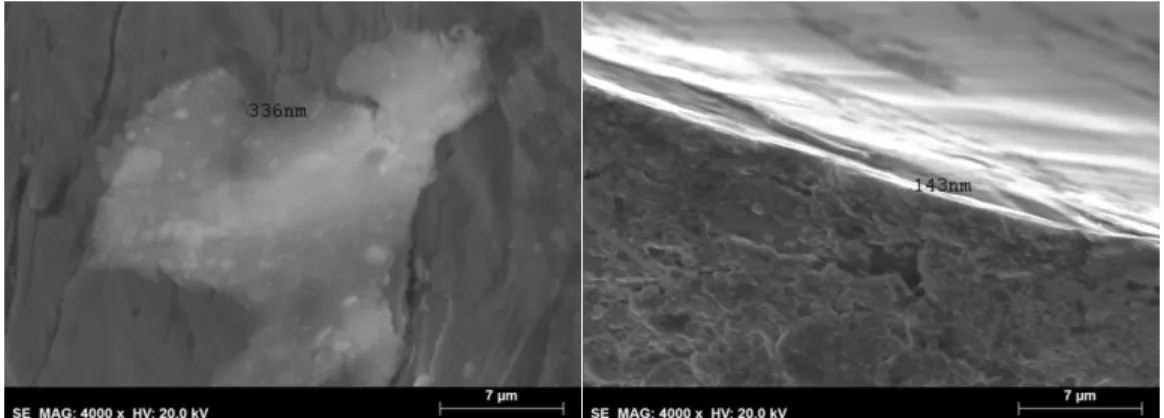
By analysing the SEM images it is possible to confirm the absence of a uniform coating
in the reaction done using NaClO and the existence of one with 238nm using K2S2O8.
5.3.
Reaction Set 3
–
Oxidant Concentration
Once the oxidant species was chosen, the effect of its concentration was studied. As can
be seen in the following table, the highest mass deposit is obtained with a 1x10⁻¹M of oxidant.
Table 14 - Mass of deposit self-assembled over the AISI304L stainless steel substrate per unit of sample area.
Set Variable
Tested [K2S2O8] /M
Deposited Mass/Sample
Area /g.cm-2
3
Oxidant
(K2S2O8)
Concentration
1x10⁻³ Below detection limit
1x10⁻² 4.72x10⁻⁶
5x10⁻² 1.74x10⁻⁵
1x10⁻¹ 3.98x10⁻⁵
2x10⁻¹ 2.60x10⁻⁵
26 The composition of the coating formed on the surface of each sample was analyzed by
Raman microscopy revealing very similar spectra. The main differences are in the relative
intensity and slight shifts in the wavelength of some peaks.
Figure 15 - Raman spectra of the surface of the AISI304L stainless steel samples exposed to the reactions of set 3.
In all these Raman spectra it is possible to observe peaks which indicate the formation
of aniline oligomers and/or polymers. Namely at 414cm-1 for 1x10⁻²M and 2x10⁻¹M and at 417cm-1 for 5x10⁻²M and 1x10⁻¹M, which correspond to the phenazine’s C-H and/or C-N-C out-of-plane wag and torsion, respectively. Other related peaks are visible at 1338cm-1 for 1x10⁻²M and 1340cm-1 for 5x10⁻²M, 1x10⁻¹M and 2x10⁻¹M, for the C~N+ stretch on phenazine or safranine-like segments; and at 1623cm-1 for 1x10⁻²M and 5x10⁻²M, and 1621cm-1 for 1x10⁻¹M 2x10⁻¹M, for the C~C wag of the benzenoid ring.
The Raman spectra also confirms the presence of sulfate ions by their visible peaks at
605cm-1 for 1x10⁻²M, 1x10⁻¹M and 2x10⁻¹M and 607cm-1 for 5x10⁻²M. All spectra show the phosphate P-O stretch vibrations in the 900-1000cm-1 region.
Figure 16 - Photos taken with the Raman microscope (50x magnification) of the surface of the samples from the reactions with 1x10⁻²M (left) and 5x10⁻²M of K2S2O8.
300
600
900
1200
1500
1800
Wavenumber /cm
-1Reaction Set 3 - [K
2
S
2
O
8
]
0.01M
0.05M
0.10M
0.20M
27
Figure 17 - Photos taken with the Raman microscope (50x magnification) of the surface of the samples from the reactions with 1x10⁻¹M (left) and 2x10⁻¹M of K2S2O8.
From the photos taken of the surface of the samples it is possible to observe that all the
reactions which yielded a measurable mass, namely those made with 1x10⁻²M, 5x10⁻²M, 1x10
-1M and 2x10⁻¹M of K
2S2O8 formed a film of PANI polymer in the emeraldine base state (blue
color).
Electrochemical charaterization of the samples was done, revealing the following
specific capacitances and potential ranges with capacitive behaviour.
Table 15 – Potential intervals and specific capacitances of the deposits formed on the surface of the AISI304L stainless steel samples exposed to the reactions of set 3.
[K2S2O8] /M Film Thickness /nm Potential Window /V Specific Capacitance /F.g-1
1x10⁻² 1560 -0.40 to 0.20 4.15x101
5x10⁻² 238 -0.30 to 0.15 1.94x10⁻³
1x10⁻¹ 743 -0.35 to 0.25 5.40
2x10⁻¹ 821 -0.43 to 0.30 1.59x101
Thus, the potassium persulfate concentration which yields the best performing capacitor
is 1x10⁻²M.
Figure 18 – SEM of the top (left) and cross-section (right) of the sample of reaction set 3 done using 1x10⁻²M of K2S2O8.