Tiago Daniel Teixeira Gonçalves
Bachelor in Micro and Nanotechnologies EngineeringImplementation of X-ray reflectivity on the
characterization of ultra-thin films for memory
devices
Dissertation submitted in partial fulfillment of the requirements for the degree of
Master of Science in
Micro and Nanotechnologies Engineering
Adviser: Joana Vaz Pinto, Assistant Professor, Faculty of Sciences and Technology, NOVA University of Lisbon
Co-adviser: Hugo Manuel Brito Águas, Associate Professor, Faculty of Sciences and Technology,
NOVA University of Lisbon
Examination Committee
Chairperson: Rui Alberto Garção Barreira do Nascimento Igreja Raporteurs: Luís Miguel Nunes Pereira
Implementation of X-ray reflectivity on the characterization of ultra-thin films for memory devices
Copyright © Tiago Daniel Teixeira Gonçalves, Faculdade de Ciências e Tecnologia, Uni-versidade NOVA de Lisboa.
Marco Polo describes a bridge, stone by stone. "But which is the stone that supports the bridge?"Kublai Khan
Acknowledgements
Em primeiro lugar gostaria de agradecer à minha orientadora Prof. Dr. Joana Pinto. Agradeço por toda a disponibilidade que demonstrou, por todas as sugestões, pelo apoio e por ter sido a melhor orientadora que poderia ter tido.
Agradeço também ao Prof. Dr. Hugo Águas por ter sido meu coorientador e por toda a ajuda essencial com a elipsometria espetroscópica bem como pelas sugestões na organização da tese.
Ao Prof. Dr. Rodrigo Martins enquanto Presidente do Departamento de Ciências dos Materiais por todo o seu esforço e empenho que levou ao sucesso que hoje o MIEMN e o DCM se podem orgulhar de ter.
À Prof. Dr. Elvira Fortunato enquanto Diretora do CENIMAT pelo seu trabalho que não só resultou numa visibilidade internacional do CENIMAT mas também por ter tornado este centro de investigação excecional.
Ao Prof. Dr. Pedro Barquinha, à Eng. Cristina Fernandes, ao Eng. Jorge Martins, à Eng. Ana Rovisco, ao Prof. Dr. Jonas Deuermeier e à Prof. Dr. Asal Kiazadeh pela ajuda na recolha de amostras e dados fundamentais para esta tese.
À Dr. Sónia Pereira pela ajuda no esclarecimento de dúvidas sobre o difratómetro. Ao Eng. Tomás Calmeiro pelas medidas de AFM bem como pela ajuda na análise das medidas.
Abstract
In this work X-ray reflectivity (XRR) was implemented as a characterization technique to study very thin films produced at CENIMAT. Three groups of samples were analysed: thin films of Ta2O5, thin films Ta2O5mixed with SiO2(TaSiO) and thin films of zinc-tin
oxide (ZTO). Spectroscopic ellipsometry was used as a complementary technique and all results were compared with the results of profilometry and Rutherford backscattering spectrometry (RBS).
A good agreement was found between the thicknesses obtained by all techniques. XRR revealed to be a better technique than SE to determine the thickness of the native oxide of silicon. In the same way the determination of the roughness was more accurate with XRR.
The objective of the characterization of the TaSiO and Ta2O5 samples was to study
the influence of the radio frequency (rf) power in the Ta2O5target during the sputtering
process. In the case of the TaSiO samples an increase of the rf power resulted in an increase of the percentage of Ta2O5 and Ar in the films, as well as an increase of the
density and dielectric constant. On the other side, the short-range order decreased. With the increase of the rf power the Ta2O5samples only revealed a lower short-range order.
The aim of the characterization of the ZTO was to study of the effect of rf power in
the ZTO target during the sputtering process, as well as the influence of the H2and O2
flows. The increase of the rf power resulted in denser films with lower short-range order. In a less clear way a change in the H2influenced the films thickness. The increase of the
O2flow had as a result films less dense and less rough.
Resumo
Neste trabalho foi implementada a técnica de refletometria de raios-X (XRR) para a carac-terização de filmes muito finos produzidos no CENIMAT. Três grupos de amostras foram analisadas: filmes finos de Ta2O5, filmes finos de Ta2O5 misturado com SiO2 (TaSiO) e
filmes de óxido de zinco e estanho (ZTO). Elipsometria espetroscópica (SE) foi utilizada como técnica complementar e os resultados foram comparados com os resultados de perfilometria e espectroscopia de retrodispersão de Rutherford (RBS).
Houve uma boa concordância entre as espessuras obtidas para todas as técnicas. XRR revelou ser uma melhor técnica do que SE para a determinação da espessura do óxido nativo das bolachas de silício. Da mesma forma, a determinação da rugosidade foi mais precisa com XRR.
O objetivo da caracterização das amostras de TaSiO e Ta2O5era estudar a influência
da potência de rádio frequência (rf) no alvo de Ta2O5durante o processo de pulverização
catódica. No caso das amostras de TaSiO o aumento da potência de rf resultou num au-mento da percentagem de Ta2O5e Ar nos filmes, assim como num aumento da densidade
e da constante dielétrica. Por outro lado, a organização a curto alcance diminuiu. Com o aumento da potência de rf as amostras de Ta2O5apenas revelaram uma diminuição da
organização a curto alcance.
A caracterização das amostras de ZTO tinha como objetivo estudar o efeito da potência de rf no alvo de ZTO durante o processo de pulverização catódica, bem como a influência do fluxo de H2e de O2. O aumento da potência de rf resultou em filmes mais densos e
com menor organização a curto alcance. De forma menos clara a mudança do fluxo de H2influenciou as espessuras dos filmes. O aumento do fluxo de O2teve como resultado
filmes menos densos e menos rugosos.
Contents
List of Figures xv
List of Tables xvii
Symbols xix
Acronyms xxi
Objectives xxiii
Motivation xxiii
1 Introduction 1
1.1 X-ray reflectivity . . . 1
1.2 Spectroscopic ellipsometry . . . 3
1.2.1 Theory . . . 3
1.2.2 Tauc-Lorentz model . . . 5
1.3 Ta2O5films . . . 5
1.4 ZTO films . . . 6
2 Methods 7 2.1 Characterization techniques . . . 7
2.2 Materials fabrication . . . 8
2.2.1 Ta2O5samples deposition process . . . 8
2.2.2 Ta2O5/SiO2samples deposition process . . . 8
2.2.3 ZTO samples deposition process . . . 8
3 Results and discussion 9 3.1 Ta2O5films . . . 9
3.2 TaSiO samples . . . 13
3.2.1 Growth rate determination (gr-TaSiO samples) . . . 14
3.2.2 Dielectric layer (d-TaSiO samples) . . . 19
3.3 ZTO samples . . . 23
3.3.1 Influence of the rf power . . . 25
3.3.2 Influence of the H2flow . . . 26
3.3.3 Influence of the O2flow . . . 27
4 Conclusions and future perspectives 29
Bibliography 31
A Abelès matrix formalism 37
C O N T E N T S
C Error functions of the performed fits 43
D Pythonfuction to convert data to be used inMOTOFIT 45
E Complementary schemes 47
F Analysis of a silicon wafer 49
G RBS analysis 51
H Parameters of the Tauc-Lorentz models obtained by spectroscopic
ellipsom-etry 53
I The real and imaginary part of the dielectric function of the ZTO samples 57
List of Figures
1.1 Data obtained by XRR of a tantalum pentoxide film on a silicon wafer. . . 1
1.2 Representation of the light interactions in a single layer system that leads to the creation of the Kiessing fringes. . . 2
1.3 Representation of the components of the electric field of a light beam [12]. . 3
1.4 Scheme of the spectroscopic ellipsometer used in this work (adapted from [12]). 4 3.1 Measured data by XRR and respective fits of Ta1 and Ta6 samples. . . 10
3.2 Comparison between the thicknesses obtained from XRR and SE. . . 11
3.3 Images of the surfaces of two samples obtained by AFM. . . 12
3.4 Real and imaginary part of the dielectric function obtained by SE. . . 12
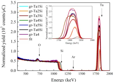
3.5 Measured data and fit of the samples gr-Ta1Si and gr-Ta6Si. . . 14
3.6 RBS spectra from all samples with the respective fits in red. . . 15
3.7 Comparison between thicknesses obtained from XRR and SE. . . 17
3.8 Real and imaginary part of the dielectric function of the samples. . . 18
3.9 RBS spectra from all samples with the respective fits in red. . . 20
3.10 Real and imaginary part of the dielectric function of the samples. . . 21
3.11 Electrical measurements of the d-TaSiO samples. . . 22
3.12 Dielectric constants obtained from the electrical measurements. . . 23
3.13 Real data and XRR fit of the sample P1-O2-H1. . . 24
3.14 Comparison between thicknesses obtained from XRR and SE. . . 25
B.1 Reflectivity panel ofMOTOFITwith the menu taps in the red boxes and the menu boxes in the green boxes. . . 39
B.2 An example of a model with fixed parameters. . . 40
B.3 Results of the SLD profile of the sample. . . 41
B.4 Results of the parameters of the sample with the respective uncertainties. . . 41
B.5 Results of the parameters of the sample with the respective uncertainties. . . 41
E.1 Model used to perform the fit of the data obtained by SE. . . 47
E.2 Scheme of the MIS structure. . . 47
E.3 Model used to perform the fit of the data obtained by SE to get the composition of the films. . . 47
F.1 Real data and XRR fit of the silicon wafer. . . 50
G.1 Fit and treated data measured by RBS from the gr-Ta5Si sample. . . 51
I.1 Real and imaginary part of the dielectric function of the samples characterized in section 3.3.1. . . 57
I.2 Real and imaginary part of the dielectric function of the samples characterized in section 3.3.2. . . 58
List of Tables
3.1 Nomenclature of the Ta2O5samples. . . 9
3.2 Thicknesses obtained from Ta2O5 samples by XRR and SE using 20.0 Å as thickness in the SE data analysis. . . 10
3.3 The roughness obtained by XRR and AFM and the SLD obtained by XRR using Si and SiO2SLD values of 18.886×10⁻⁶and 20.124×10⁻⁶Å−2respectively. . 11
3.4 Nomenclature of both gr-TaSiO and d-TaSiO samples. . . 13
3.5 Results of the RBS fits. . . 15
3.6 Thicknesses obtained by profilometry, XRR, SE and RBS. . . 16
3.7 Calculated growth rates based on the obtained thicknesses. . . 16
3.8 Results from XRR and SE data analysis of the Ta2O5and of the native oxide using Si and SiO2SLD values of 18.886×10⁻⁶ and 20.124×10⁻⁶Å−2 respec-tively. . . 17
3.9 Thicknesses obtained by SE and RBS. . . 19
3.10 Composition in molecular % obtained by RBS and SE data analysis. . . 20
3.11 Thicknesses of the native oxide and roughnesses of the Ta2O5. . . 21
3.12 Samples nomenclature used in function of the fabrication parameters. . . 23
3.13 Results from XRR and SE data analyses of the samples with different target rf power using Si and SiO2SLD values of 18.886×10⁻⁶ and 20.124×10⁻⁶Å−2, respectively. . . 25
3.14 Results from XRR and SE data analyses of the samples with different H2flow using Si and SiO2SLD values of 18.886×10⁻⁶and 20.124×10⁻⁶Å−2, respec-tively. . . 26
3.15 Results from XRR and SE data analyses of the samples with different O2flow using Si and SiO2SLD values of 18.886×10⁻⁶and 20.124×10⁻⁶Å−2, respec-tively. . . 27
C.1 χ2of the fits performed in the Ta2O5samples (section 3.1). . . 43
C.2 χ2of the fits performed in the TaSiO samples (section 3.2). . . 43
C.3 χ2of the fits performed in the ZTO samples (section 3.3). . . 43
F.1 Results of XRR and SE analyses of a silicon wafer using Si and SiO2SLD values of 18.886×10⁻⁶and 20.124×10⁻⁶Å−2, respectively. . . 49
G.1 Results from the performed fit of the gr-Ta5Si sample. . . 51
H.1 Parameters from a Tauc-Lorentz oscillator of Ta2O5samples (section 3.1). . . 53
H.2 Parameters from a double Tauc-Lorentz oscillator of TaSiO samples used to determine the grow rate (section 3.2.1). . . 53
H.3 Parameters from a double Tauc-Lorentz oscillator of TaSiO samples used as a dielectric material (section 3.2.2). . . 54
L i s t o f T a b l e s
H.5 Parameters from a double Tauc-Lorentz oscillator of ZTO samples in the study of the influence of the H2flow (section 3.3.2). . . 55
H.6 Parameters from a double Tauc-Lorentz oscillator of ZTO samples in the study of the influence of the O2flow (section 3.3.3). . . 55
Symbols
∆ Change in the polarization of the light after the interaction with the
material.
ψ Change in the amplitude of the components of the electric field after
the interaction with the material.
λ Wavelength.
θ Angle.
χ2 Error function.
ε∞ High frequency dielectric constant.
ε1 Real part of the dielectric function.
ε2 Imaginary part of the dielectric function.
αc Critical angle.
σn,n+1 Roughness or diffusenes of a layer.
A Transition matrix element. C Broadening term.
E Photon energy.
E0 Peak transition energy.
Eg Band gap energy.
Q Momentum transfer.
dK Distance between two peaks of the Kiessing fringes.
kz Wave factor.
rp Amplitude reflection coefficients of the incident parallel polarized
wave.
rs Amplitude reflection coefficients of the incident perpendicularly
Acronyms
AFM Atomic Force Microscopy.
CENIMAT Materials Research Center.
DRAM Dynamic Random Access Memory.
GIZO Indium-Gallium-Zinc Oxide.
MIS Metal-Insulator-Semiconductor.
RBS Rutherford Backscattering Spectrometry.
rf radio frequency.
RRAM Resistive Random Access Memory.
SE Spectroscopic Ellipsometry. SLD Scattering Length Density.
TaSiO mixture of Ta2O5and SiO2.
TFT Thin-Film Transistor.
XRR X-ray Reflectivity.
Objectives
Nowadays the memory devices are based on thin films that are becoming even thinner. However the development of thinner films leads to a problem: the characterization of those films. With thicknesses that can be lower than 10 nm, the implementation of tech-niques capable of measure such thicknesses are crucial in order to continue the scientific research in the field of memory devices.
Taking that in mind the main objective of this work was the implementation of X-ray Reflectivity (XRR) to characterize thin and ultra-thin films at Materials Research Center (CENIMAT). Some of the XRR experiments were performed before the beginning of the thesis but due to the lack of a data analysis method, the determination of the properties of the films was not possible. The implementation of such method turned possible the use of XRR at CENIMAT. By using spectroscopic ellipsometry (SE) one aimed to confirm the success of the XRR data analysis method as well as study the limitations and information one can get from both techniques.
To test the analysis method, some sets of samples of the research group were analysed. Films of Ta2O5mixed with SiO2, Ta2O5and zinc-tin oxide (ZTO) were used. The variation
of the used radio frequency power in the target during the sputtering process was studied in all samples. In the ZTO samples the variation of the H2and O2was also studied.
Motivation
One must do everything that is possible with the available resources. That was the spirit behind this work. CENIMAT has a diffractometer that enables XRR characterization.
The implementation of a protocol to analyse the XRR measured data would turn possi-ble the use of the diffractometer for another characterization technique (besides X-ray
Diffraction) with no additional costs.
Besides that, until the beginning of this thesis the characterization of some thin films produced at CENIMAT had been a challenge. Semiconductor films for thin-film transis-tors with thicknesses between 20 and 40 nm, dielectric and semiconductor films produced by solution process and storage layers in memory devices below 10 nm are some examples where other characterization techniques can not be successfully used.
C h a p t e r
1Introduction
1.1 X-ray reflectivity
Nanostructured devices are becoming more used in many fields like microelectronics, optoelectronics and sensors. These devices use thin films that are becoming thinner with the evolution of fabrication processes. With this reduction of thickness and with the use of multilayers films, some physical properties of the films and their interfaces become crucial for the correct function of the devices [1].
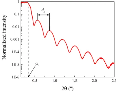
X-ray Reflectivity (XRR) is a non-destructive method of characterization that can analyse crystalline and amorphous single and multilayer thin films. This technique takes advantage of the fact that matter has a refractive index for X-rays smaller than one. As a result, for angles below a specific critical angle, the incident X-rays are reflected. In other words, occurs a total external refraction. This physical property makes it possible to get information about the material density. Besides that, with this technique it is possible to obtain the film thickness (precision below 1 nm) and the roughness of the surface and interfaces [1, 2].
The critical angle (αc) can easily be obtained from the angle from which the measured
intensity drops rapidly. After being obtained, the critical angle can be used for a density analysis. The thickness of a film can also be easily obtained and this parameter is related to the angular distance between oscillation waves in the intensity of reflected light -Kiessing fringes (dK) [1]. As an example, a XRR curve is plotted in Figure 1.1 illustrating
the determination of theαcanddK.
Figure 1.1: Data obtained by XRR of a tantalum pentoxide film on a silicon wafer.
C H A P T E R 1 . I N T R O D U C T I O N
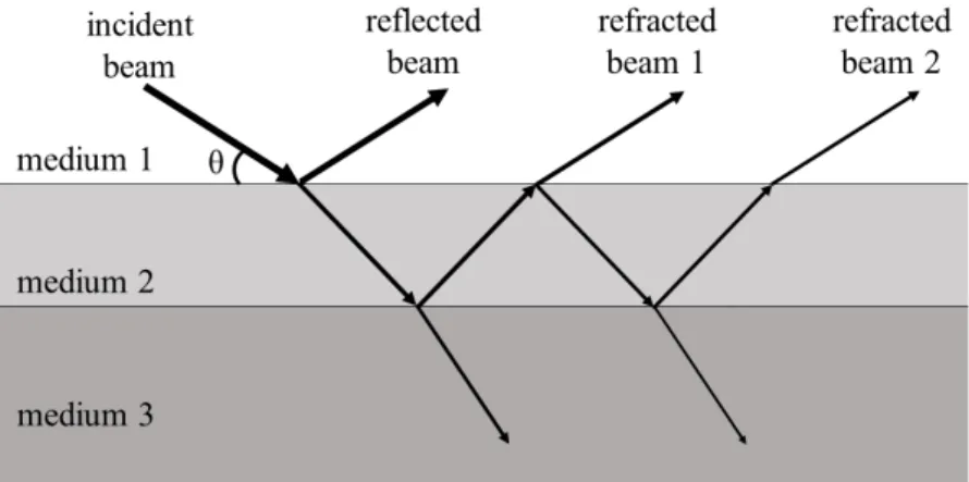
is reflected and other the part penetrates the film. The part of the beam that penetrates the film will be divided again: part will be reflected in the interface between medium 2 and 3 and part will penetrate the medium 3 and so on. All the components of the initial incident beam that will go out to medium 1 will interact with each other [3]. Here it is considered just the specular part of the beam (when the angle of the incident beam is equal to the angle of the reflected beam) [1].
Figure 1.2: Representation of the light interactions in a single layer system that leads to the creation of the Kiessing fringes.
It is usual to use mathematical formalism to analyse the measured data. In this work the analyses of XRR data were performed in the MOTOFIT package [4]. This package uses the Abelès matrix formalism [5]. In Appendix A is possible to find more information this formalism.
There are a few set-ups that can be used to perform XRR analyses. In the set-up used in this work both the X-ray source and the detector moved and the sample is kept fixed. The other possibility in rotate the sample at the same time as the source moves. In this case the detector is fixed. Nevertheless, in these two set-ups the angle between the source-sample and sample-detector is the same, as one only uses the specular part of the reflected beam [1, 2].
Despite same differences, in all set-ups a high intense X-ray source and a low noise
detector is necessary. This is due the fact that the range of orders of magnitude of the measure intensity can be higher than 5. In the example shown in Figure 1.1 the range of the measured intensity has almost 6 orders of magnitude. Not only that but the alignment of the sample is crucial and should be performed carefully [1, 2].
In this thesis XRR was used only to know thicknesses, roughnesses and Scattering Length Density (SLD) (a parameter proportional to the mass density) in a dry medium. Despite that, XRR has been used in more applications. For example, XRR can be used to study layers in a liquid medium [6] as well as liquid-liquid and air-liquid interfaces [7], to do image reconstruction of the samples [8], to determine the element depth profiles in low contrast multilayers systems [9], to determine the electron density profile of a electrolyte solution inside nanotubes [10] or even to calibrate ellipsometers [11].
1 . 2 . S P E C T R O S C O P I C E L L I P S O M E T RY
1.2 Spectroscopic ellipsometry
1.2.1 Theory
Ellipsometry is a non-destructive optical characterization technique that characterizes light that is reflected from a sample. It can also characterize transmitted light, but this work focuses only on the reflection mode. It measures the change that occurs in the po-larization of light with the interaction light-material. This technique is named «ellipsom-etry» because, with this interaction, linearly polarized light usually becomes «elliptical» [12].
Light is an electromagnetic wave composed by an electric field and a magnetic in-duction which are perpendicular to each other. The electric field is used to describe the polarization state of light. For that, when a light beam is travelling along thezaxis, its
associated electric field can be decomposed in two components: one parallel to thexaxis and another parallel to they axis (Figure 1.3a). These components are described by the
propagation number (that depends on the wavelength), their initial magnitude and initial phase [12].
(a) Linear polarization (b) Elliptical polarization
Figure 1.3: Representation of the components of the electric field of a light beam [12].
The polarization state is directly correlated with the difference between the two
com-ponents, in the amplitude and in phase. When there is no difference in the initial phases
the result is an electromagnetic wave with planar polarization state. When this difference
is not zero, the synthesized vector rotates with the propagation of light, which results in an elliptical polarization (Figure 1.3b). The particular case when the difference is equal
toπ/2 the polarization state is circular [12].
With the interaction with matter, the phase of the electric field can change and this change depends on the refraction index. Because of that, one of the values measured in ellipsometry to characterize the sample is the change in the polarization of the light, witch is represented by∆[12].
C H A P T E R 1 . I N T R O D U C T I O N
tg(ψ) =rp
rs
(1.1)
whererp andrsare the amplitude reflection coefficients of the incident parallel polarized
wave (rp) and the perpendicularly polarized wave (rs) to the plane of incidence. These
coefficients are given by Fresnel equations [12].
These two values (ψ,∆) express the change in phase and amplitude that appends in light with the reflection on the sample. So, in ellipsometry, the change in the emitted light is measured as the change in the polarization state and this is represented by the fundamental equation of ellipsometry [12]:
ρ=tg(ψ)exp(i∆) (1.2)
If one takes as an example a simple structure,ψcharacterize the refractive index of the
sample and∆describes the extinction coefficient. Therefore, these two values measured
by Spectroscopic Ellipsometry (SE) describe directly two properties of the sample. This example represents the basic principle of elipsometry [12].
Until here, it has been described the ellipsometry technique, however in this work it was used SE that has the same fundaments of the ellipsometry but uses a light spec-tra instead of a monochromatic light. Using SE today it is possible to determine many physical properties of the sample with the two values measured (ψ,∆) as function of the wavelength or energy, namely the complex refractive index, complex dielectric function, absorption coefficient, film thickness, band gap and free-carrier absorption. To obtain
these properties, it is necessary to create optical models to analyse the SE data. For the creation of those models, it is crucial to have as much information as possible of the sample, like approximate thicknesses and materials [12].
A spectroscopic ellipsometer is required to do SE analyses. In the system used in this thesis, the light ray comes from a polychromatic light source, passes through a linear polarizer and then the sample is subjected to this incident light. After the reflection, light (now elliptical polarized) passes through a periodic modulator and an analyser. Finally, light reaches the detector that measures the intensity of light [12]. A scheme of this system can be found in the figure below.
Figure 1.4: Scheme of the spectroscopic ellipsometer used in this work (adapted from [12]).
1 . 3 . TA2O5 F I L M S
1.2.2 Tauc-Lorentz model
In order to analyse the experimental data, one needs a mathematical function. One of the most well-known is the Tauc-Lorentz dispersion formula [13]. This formula is the junction of the Tauc joint density states [14] and the Lorentz calculation of the imaginary part of the dielectric function (ε2) [15]. This is given by [13]:
ε2(E) =
AE0C(E−E0)2
E2−E02+C2E2 1
E , E > Eg
0, E≤Eg
(1.3)
whereAis the transition matrix element,Cis the broadening term,Eis the photon energy, E0is the peak transition energy andEg is band gap. All these parameters are in energy
units and, exceptE, are fitting parameters. Eis the variable and the fitting is performed
as function ofE.
Doing a Kramers–Kronig integration of the equation 1.3 it is possible to obtain the real part of the dielectric function. With this integration a new fitting parameter appears,
ε∞, which represents the high frequency dielectric constant [13].
1.3 Ta
2O
5films
Given the decrease of devices dimensions, it is important to find materials with high dielectric constant to be an alternative to SiO2[16–18]. One of the most studied materials
is the Ta2O5 that has a high dielectric constant, high refractive index [19, 20] and has
been studied using both XRR [21–23] and SE [17, 24–27]. Due to its properties, Ta2O5
has been used in several applications such as Dynamic Random Access Memory (DRAM) [19, 28] and redox-based Resistive Random Access Memory (RRAM) [29].
Taking into account the number and diversity of applications, it is crucial to under-stand the relation between the fabrication methods and the film’s properties. For example, a change in the dielectric constant of Ta2O5with variations in the deposition process has
already been reported [30, 31]. Furthermore, for the Ta2O5application as redox-based
RRAM has been shown that the change in the film density can affect the device behaviour
[32].
In order to improve the properties of Ta2O5 films to be used as dielectric layer in
transistors, a mixture of Ta2O5and SiO2(TaSiO) can be used. TaSiO film presents a lower
leakage current, a lower hysteresis magnitude and a faster recovery of the threshold voltage, compared to a Ta2O5 film. Besides that, the use of a substract bias can even
lower the leakage current. So, using a mixture with SiO2and substract bias, one can have
thinner films and with better properties [24, 33].
In this work TaSiO films were produced by radio frequency (rf) co-sputtering with subtract bias. The objective was to study the influence of the rf power in the Ta2O5target
C H A P T E R 1 . I N T R O D U C T I O N
nature was performed in Ta2O5films, also produced by rf sputtering with subtract bias.
The fabrication conditions were the same for both studies to be possible to compare the results.
1.4 ZTO films
Thin-Film Transistor (TFT) is a device with many applications such as displays and solar cells. In order to have a better performance of TFTs for this application, amorphous oxide semiconductor has been studied to substitute technologies like a-Si:H TFTs. This is due to the excellent uniformity in large areas, high transparency and good electric performance [34–36].
Indium-Gallium-Zinc Oxide (GIZO) is one of the amorphous oxide semiconductors used. This material presents a good electrical performance in displays and solar cells and can be fabricated at room temperature [35]. However, according to a report published in January 2018 by the European Commission [37], both indium and gallium are in the list of critical raw materials and have an end-of-life recycling input rate close to 0 %. So, indium- and gallium-free TFTs have been studied.
Zinc-Tin Oxide (ZTO) has been widely studied as an alternative to GIZO due to its performance and the fact that it does not use critical raw materials. It presents many advantages such as being cheap, non-toxic, having good physical robustness, film smooth-ness, chemical stability and good transparency [38–42]. Recently was shown that ZTO can be used to fabricate flexible TFTs at low temperature. Not only that but it was also demon-strated that the electric performance of the TFTs is improved with the incorporation of hydrogen in the ZTO layer [34].
In the present work ZTO films were produced using different parameters. With this
approach one aimed to study the influence of parameters like H2and O2flow during the
rf sputtering fabrication in the density, roughness and thickness of the films.
C h a p t e r
2Methods
2.1 Characterization techniques
XRR was performed using the PANalytical’s X’Pert PRO MRD X-ray diffractometer with
a monochromatic source of CuKα(λ= 1.540598Å). To perform a XRR analysis both the
X-ray source and detector move, changing the angle (θ) relatively to the sample. The
2θscan range used in this work was from 0.1000° to 4.0000° with a step size of 0.0050°.
With this analysis one can take the thickness, roughness and SLD for each film. The data analysis was done in theMOTOFIT 4.1package [4]. A tutorial of the data analysis can be found in Appendix B and all error functions of the performed fits in the Appendix C.
However, the files obtained by XRR cannot be directly used inMOTOFIT 4.1. As an output, the diffractometer gives the angle (2θ) and the respective measured intensity. As
an input,MOTOFIT 4.1needs the photon momentum as well as the respective normalized intensity. To create files with the data properly converted, a function was made inPython 3.6.3. The code is in Appendix D.
To obtain the real and imaginary part of the dielectric function a HORIBA-Jobin Yvon Uvisel spectroscopic ellipsometry system was used with an incident angle of 70° and in a spectral range between 1.5 and 6.5 eV. The acquired data was analysed withDeltaPsi 2software (HORIBA) and all error functions of the performed fits can be found in the Appendix C.
The models used to analyse the SE data were composed by the following layers: crys-talline silicon as a substract, SiO2(silicon native oxide), the material to be analysed and a
roughness layer (50 % of void and 50 % of the material) (Figure E.1). For the crystalline silicon it was used a reference model of the software. The model of the SiO2was fitted
using the Tauc-Lorentz dispersion formula [13] at the same time as its thickness (with an initial guess of 20 Å) from a silicon wafer. Then, that model of the SiO2 was used
in all samples without fitting. For the films to be analysed both the parameters of the Tauc-Lorentz dispersion formula [13] and thickness were fitted. The initial guesses for the thicknesses were the thicknesses obtained by the other techniques or the values one expected from the fabrication methods. In the samples where the thickness of the rough-ness layer was close to 0.1 Å the layer was not used because that is the lower result of a
thickness fitting, so it is meaningless.
In order to have a more direct measurement of the roughness of the film, Atomic Force Microscopy (AFM) analyses were performed using Asylum MFP-3D system in tap-ping mode. The AFM images analysis were done in the Gwyddionsoftware. Also, to have a more direct measure of some film thicknesses, a XP-200 profilometer from Am-bios Technology were used. The compositions of the films were obtained by Rutherford Backscattering Spectrometry (RBS) using a 2.5 MV van de Graaf Accelerator with a 2 MeV
He+beam. The RBS spectra were analysed with the IBA DataFurnace NDF software [43].
C H A P T E R 2 . M E T H O D S
The characterization of the Metal-Insulator-Semiconductor (MIS) devices were per-formed in Keysight B1500A Semiconductor Device Analysis. A scanning range from 5 to −11 V with a frequency of 100 kHz were used. The metal contact was made of molybde-num and was the grounded contact (Figure E.2).
2.2 Materials fabrication
2.2.1 Ta2O5 samples deposition process
The first samples to be analysed were Ta2O5films. With this samples one aimed to study
the influence of rf power in the Ta2O5target in the density and roughness of the films
and to assess how XRR can be used to extract information. In order to achieve that, six samples were prepared with a range of 0.31 to 1.85 Wcm−2rf power in the Ta
2O5target.
All films were deposited in pieces of a 4′′ p-type silicon wafer with a resistivity from
1 to 2Ωcm by rf sputtering from a 2′′Ta
2O5target. The deposition pressure was 0.3 Pa
and a flow ratio of Ar/O2was 14/1. It was also used a 15 W sample bias.
A piece of the same wafer was analysed to obtain the SiO2thickness. The goal was to
be sure of the most amount of properties possible so one has less fitting parameters in the SE and XRR data analysis.
2.2.2 Ta2O5/SiO2samples deposition process
Two sets of samples were produced with two different objectives. The main goal was to
produce films to be used as the dielectric material in transistors and in MIS capacitors. Here a thickness of 250 nm were desired for the dielectric layer. In order to achieve that, a first set of samples were fabricated to calculate the growth rate of the films. Knowing the growth rate, a second set of samples were produced with the desired thickness of 250 nm.
The deposition process of these samples was similar to the Ta2O5samples.
Neverthe-less these films were deposited by rf co-sputtering from a 2′′ Ta
2O5and a 2′′ SiO2AJA
systems targets. Besides that, six samples for each set were produced with a rf power of 1.23 Wcm−2in the SiO
2target and in a range of 0.31 to 1.85 Wcm−2in the Ta2O5target.
A sample with only Ta2O5was also produced with a rf power of 1.23 Wcm−2.
2.2.3 ZTO samples deposition process
In order to study the influence of hydrogen in ZTO films to be used as the dielectric layer in TFTs, several films were produced at different fabrication conditions.
All films were fabricated in a 4′′ p-type silicon wafer with a resistivity from 1 to
2Ωcm by rf sputtering from a 2′′ ZTO AJA systems target. The time of pre-sputtering
used was 15 min, the deposition pressure of 0.3 Pa with 50 sccm of Ar flow. The conditions
that changed between samples were: the rf power in the target (combined with a change of the deposition time) and the flow of both O2and H2.
C h a p t e r
3Results and discussion
3.1 Ta
2O
5films
The first set of samples considered here consisted of Ta2O5films grown by rf sputtering
on silicon. These films are usually used as the dielectric layer in devices such as TFTs at Materials Research Center (CENIMAT). This set of samples was produced with different
rf powers (from 0.3 to 1.85 Wcm−2) in the Ta
2O5 target during the sputtering process
and using a substrate bias of 15 W. With this it was aimed to study the influence of the rf power in the fabricated films.
In the following table it is possible to found the nomenclature used in the section. The nomenclature was chosen in function of the rf power.
Table 3.1: Nomenclature of the Ta2O5samples.
Sample Rf power (Wcm−2)
Ta1 0.30 Ta2 0.62 Ta3 0.93 Ta4 1.23 Ta5 1.54 Ta6 1.85
Before the characterization of the Ta2O5films, a piece of the same silicon wafer was
characterized. The objective was to lower the number of the fitting parameters of the data analysis. The analysis of the silicon wafer can be found in Appendix F. With that analysis one concluded that it is possible to use a native oxide thickness of 20 Å in the SE data analyses.
An important remark about the XRR is that it was used the theoretical SLD of Si and SiO2: 18.886×10⁻⁶and 20.124×10⁻⁶Å−2, respectively (more details in Appendix F). The XRR data was analysed using the procedure presented in Appendix B.
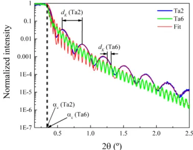
In Figure 3.1 it is possible to see the measured data of two samples with the respective fits: the sample with a low rf power (Ta2) and the sample with a high rf power (Ta6). Just with this figure it is noticed that the sample Ta1 should have a similar density to the sample Ta6 because it has a similar critical angle (αc). However, it has a bigger distance
between two peaks of the Kiessing fringes (dK) so it is clearly thinner. The results of the
C H A P T E R 3 . R E S U LT S A N D D I S C U S S I O N
Figure 3.1: Measured data by XRR and respective fits of Ta1 and Ta6 samples.
The first parameter that will be discussed is the thickness of the Ta2O5 films. The
obtained thicknesses are shown in Table 3.2. As one can see both techniques are in excellent agreement and the results for the thickness have a very low uncertainty. This is the first sign of the success of the implementation of XRR. Nevertheless, it is worth to point out a discrepancy in the case of the thickness of the Ta1 sample. This will be discussed later.
Table 3.2: Thicknesses obtained from Ta2O5samples by XRR and SE using 20.0 Å as thickness in
the SE data analysis.
Sample Deposition time (min)
Ta2O5thickness
(Å)
Ta2O5growth
rate (Å/min)
SiO2thickness
(Å)
XRR SE XRR SE XRR
Ta1 30 19.1 ± 0.4 28.9 ± 0.3 0.64 0.96 17 ± 8
Ta2 30 133.3 ± 0.9 136 ± 2 4.4 4.5 18 ± 3
Ta3 26 316 ± 2 319 ± 2 12.2 12.3 18 ± 11
Ta4 20 238.2 ± 0.6 232 ± 2 11.91 11.61 17 ± 3
Ta5 20 573 ± 1 572 ± 3 28.7 28.6 18 ± 5
Ta6 20 718 ± 2 718 ± 5 35.9 35.9 19 ± 6
1The flow ratio of Ar/O
2used to grow this sample was 14/3 instead of 14/1 and
this may be the explanation for a smaller growth ration.
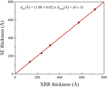
To have a better view of the differences between the thicknesses obtained by SE and
XRR, a representation of the thicknesses obtained by both techniques is presented in Figure 3.2. A linear fit was performed in order to compare these differences with the
results reported in the literature (witout the thickness of Ta1 sample). The result of this fit revealed to be similar to the ones described in the literature [11, 44–46]: there is a clear
3 . 1 . TA2O5 F I L M S
linear tendency and the slope of the linear fit is near 1. Besides that the interception is equal to 0.
Figure 3.2: Comparison between the thicknesses obtained from XRR and SE.
Besides the thickness of the Ta2O5, the thickness of the native oxide was also fitted
in the XRR data analysis. The results (see Table 3.2) are very consistent between samples when one takes in consideration the associated uncertainty. Not only that, but the results are also similar to the 20 Å used as the thickness of the native oxide in SE data analysis.
The thicknesses of both the Ta2O5and the native oxide were not the only fitted
pa-rameters. The SLD and roughness of the samples were also fitted. Previously, with only the representation of the XRR data of the samples Ta2 and Ta6 (Figure 3.1) one concluded that the density should not be changing with the increase of the rf power in the target.
In Table 3.3 the results of the fits are presented and the same conclusion can be taken: no evidence of a change in the density of the samples was found for different values of rf
power. This is true not only for the density, but also for the roughness of the films that were obtained by XRR and AFM (here SE did not give viable results).
Table 3.3: The roughness obtained by XRR and AFM and the SLD obtained by XRR using Si and SiO2SLD values of 18.886×10⁻⁶and 20.124×10⁻⁶Å−2respectively.
Sample SLD (10
−6Å−2) Ta
2O roughness (Å)
XRR XRR AFM
Ta1 48 ± 9 5.0 ± 0.5 2.8
Ta2 49 ± 3 3.4 ± 0.2 4.2
Ta3 48 ± 3 4 ± 2 4.2
Ta4 48 ± 2 5.1 ± 0.5 3.7
Ta5 50 ± 4 5 ± 2 3.3
C H A P T E R 3 . R E S U LT S A N D D I S C U S S I O N
From the AFM images used to get the roughness of the samples, one can see how smooth and regular the surfaces of the films are. As an example, two of those images are show below. The small dots in the surfaces may be impurities acquired by the exposition of the samples to the air.
(a) Ta2 (b) Ta6
Figure 3.3: Images of the surfaces of two samples obtained by AFM.
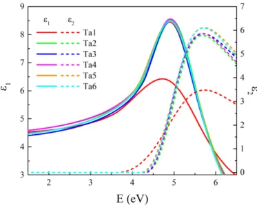
As previously said, with the XRR analysis one concluded that the SLD of the samples did not change with the variation of the rf power. In other words, the density remained unchanged. The same conclusion can be made with the analysis of the Tauc-Lorentz models obtained to describe the samples. This is shown in Figure 3.4 where the real and imaginary part of the dielectric function (ε1 andε2, respectively) are represented
as functions of the photon energy. The models for these two properties are very similar for all samples, except for the Ta1 sample(Table H.1). This may be the reason for the difference in the thickness determined by SE and XRR of this sample.
Figure 3.4: Real and imaginary part of the dielectric function obtained by SE.
3 . 2 . TA S I O SA M P L E S
For the other samples a change in density is not found, as the maximum ofε2 does
not clearly change [47]. Besides that, it is possible to notice that in all samples the Ta2O5
is amorphous, because the increase of theε2with the photon energy is not abrupt [26].
Furthermore, from the parameters of the Tauc–Lorentz model (Table H.1) it is possible to conclude that the increase of the rf power in the Ta2O5target leads to a small decrease
of the band gap of the films and a decrease of short-range order (increase in C) [17, 47]. Again, no difference in the parameterAwas found, so the density of the films did
not change with different values of the rf power in the Ta2O5 target [17, 47], which is
consistent with the results of the XRR data analysis.
To summarise, with this set of Ta2O5samples grown by rf sputtering it was possible
to conclude that: no difference in the density and roughness of the films was found with
the variation of rf power in the Ta2O5target, the increase of the rf power decreased the
band gap and short-range order of the films and all samples were amorphous.
3.2 TaSiO samples
After the successful implementation of XRR and the use of the procedure presented in Appendix B to characterize Ta2O5films, one aimed to use this technique to characterize
more complex samples. So, the second and third sets of samples that were characterized consisted in a mixture of Ta2O2and SiO2compound films (TaSiO) for a dielectric study
performed in CENIMAT. The films were grown by co-sputtering and different rf powers
were used on the Ta2O2target to achieve samples with different compositions.
Two sets of samples were analysed: films used to determine the growth rate of the specific target powers (named gr-TaSiO) and films used for the dielectric layer in TFTs and MIS devices, where the thickness of all layers were set to be approximately 250 nm (named d-TaSiO). In the following table the nomenclature and the details of the deposition process of each sample is presented. The used nomenclature was set based on the rf power and composition of each sample.
Table 3.4: Nomenclature of both gr-TaSiO and d-TaSiO samples.
Sample Rf power (Wcm−2)
growth rate determination
dielectric
layer Ta2O5target SiO2target
gr-Ta1Si - 0.30 1.23
gr-Ta2Si d-Ta2Si 0.62 1.23
gr-Ta3Si d-Ta3Si 0.93 1.23
gr-Ta4Si d-Ta4Si 1.23 1.23
gr-Ta5Si d-Ta5Si 1.54 1.23
gr-Ta6Si d-Ta6Si 1.85 1.23
C H A P T E R 3 . R E S U LT S A N D D I S C U S S I O N
3.2.1 Growth rate determination (gr-TaSiO samples)
Since these samples were produced to determine the growth rate, the thickness is the most important parameter to be measured. For this set of samples four techniques were used to do so: profilometry, XRR, SE and RBS.
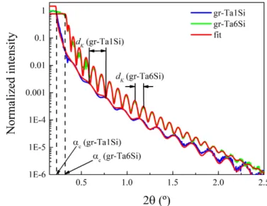
As in the previous section, an important remark about the XRR needs to be done. Since the fit of the SLD of the native oxide and silicon were not possible to perform, the theoretical SLD of Si and SiO2used were 18.886×10⁻⁶and 20.124×10⁻⁶Å−2respectively (more details in Appendix F). Despite that it is possible to see in Figure 3.5 de quality of the fits. Just with the information found in the figure below, it is possible to predict that the increase of rf power in the Ta2O5leads to thicker samples because the sample
gr-Ta6Si has a bigger distance between two peaks of the Kiessing fringes (dK) and leads
to denser samples since the critical angle (αc) is higher in the sample gr-Ta6Si.
Figure 3.5: Measured data and fit of the samples gr-Ta1Si and gr-Ta6Si.
Taking this remark in mind for the XRR data analysis the thickness in length units is a parameter that can be fitted. The same happens in the SE data analysis. For the other techniques the thickness is obtained in a different way. On one hand, by profilometry
the thickness is obtained directly with the measure in length units. On the other hand, with RBS the thickness is a fitting parameter, but it is expressed in atomscm−2and to be
converted to length units one must to consider the film’s density.
The RBS spectra with the obtained fits with the energy barriers indicated for each element is shown in Figure 3.6. It was needed to assume a fixed stoichiometry for the tantalum and silicon oxides in order to extract a relative concentration of each oxide. In other words, the fit was not done for the elements but for the molecules (it was assumed that the both components formed a solid solution). Looking at the figure bellow one can see that the number of counts for the peak of Ta is increasing with the increase of the rf power in the target. This means that the quantity of Ta is also increasing.
3 . 2 . TA S I O SA M P L E S
Figure 3.6: RBS spectra from all samples with the respective fits in red.
The same result can be seen in Table 3.5 where the results of the fits are presented. The molecular % of Ta2O5is increasing relatively to the molecular % of SiO2. The molecular
% of Ar remains between 3 and 5 % for almost all samples.
Table 3.5: Results of the RBS fits.
Sample (atomscmThickness−2) Ta2O5(%) SiO2(%) Ar (%)
gr-Ta1Si 38.0 25.5 66.4 8.1
gr-Ta2Si 251.0 31.4 65.8 2.8
gr-Ta3Si 374.0 40.8 40.8 3.8
gr-Ta4Si 500.0 67.3 29.1 5.0
gr-Ta5Si 377.5 70.1 25.5 3.3
gr-Ta6Si 376.4 72.0 24.5 3.5
gr-Ta4 390.0 95.2 - 4.8
However, as previously said, since one wants to compare the thickness obtained by this technique with the others it is fundamental to convert the thickness from atomscm−2
to length units, in this case Å. To do so the procedure in Appendix G was followed. One needs to take in mind that for the conversion it was necessary to use the mass densities of the components 2.2 and 8.2 gcm−3for the Ta
2O5and SiO2, respectively [48].
C H A P T E R 3 . R E S U LT S A N D D I S C U S S I O N
explained by the difficult fitting of the measured data of films with such a low thickness.
Table 3.6: Thicknesses obtained by profilometry, XRR, SE and RBS.
Sample
Film thickness (Å)
profilometry XRR SE RBS
gr-Ta1Si (24 ± 3)×10 212 ± 4 0.20 ± 0.05 55 ± 3 gr-Ta2Si (32 ± 4)×10 330.8 ± 0.5 266 ± 4 358 ± 18 gr-Ta3Si (57 ± 3)×10 497 ± 4 507 ± 3 511 ± 26 gr-Ta4Si (73 ± 5)×10 672 ± 5 678 ± 5 670 ± 34 gr-Ta5Si (52 ± 4)×10 451 ± 4 462 ± 2 503 ± 26 gr-Ta6Si (46 ± 3)×10 445 ± 4 458 ± 2 501 ± 26
gr-Ta4 - 505 ± 2 507 ± 4
-Despite the results being similar, the thickness from RBS are slightly different in some
cases relatively to the thicknesses obtained by XRR and SE. Three main reasons can be pointed out. The first one is that the fits were from the molecules and not the elements and the stoichiometry can be different from the stoichiometry assumed. The second one
is that the mass density assumed may not be the right one. Finally, the fits are not perfect and one sign of that is that the molecular % of Ar is not consistently increasing with the increase of the rf power. Nevertheless, the difference between techniques is very small.
With the thicknesses determined it is possible to calculate the growth rates as one can see in Table 3.7. At the time the d-TaSiO samples were fabricated, only the thicknesses obtained by profilometry were known. This does not represent a problem because the growth rates calculated based on the four techniques are very close to each other.
Table 3.7: Calculated growth rates based on the obtained thicknesses.
Sample Depositiontime (min)
Growth rate (Å/min)
profilometry XRR SE RBS
gr-Ta1Si 30 8.0 7.1 - 1.8
gr-Ta2Si 30 10.7 11.0 - 11.9
gr-Ta3Si 30 19.0 16.6 16.9 17.0
gr-Ta4Si 30 24.3 22.4 22.6 22.3
gr-Ta5Si 15 34.7 30.1 30.8 33.5
gr-Ta6Si 12 38.3 37.1 38.2 41.8
gr-Ta4 30 - 16.8 16.9
-Although the main objective has already been achieved, more analyses can be done with these samples. One relation that can be study is the relation between the thicknesses obtained by XRR and SE data analysis presented in Figure 3.7. The result is similar to the results reported in literature [11, 44–46]: there is a clear linear tendency, the slope of the
3 . 2 . TA S I O SA M P L E S
linear fit is near 1 and the interception is different than 0. Interceptions different than 0
have been reported in different studies but this fact remains without a good explanation
[45].
Figure 3.7: Comparison between thicknesses obtained from XRR and SE.
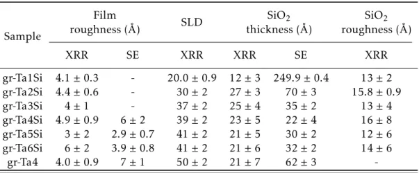
Continuing the comparison between XRR and SE results, an agreement is not found in the roughness of the films (Table 3.8). The roughnesses obtained by XRR seems to be very similar for all samples. The same does not happen with the SE data analysis. Not only that, but by SE it was not possible to determine the roughnesses of some films because those values tended to 0.1 Å, which is the limit of the used software, so those values were
meaningless. In those cases, no roughness layer was used in the data analysis. Here XRR revealed to be a more useful technique to measure the film roughness.
Table 3.8: Results from XRR and SE data analysis of the Ta2O5and of the native oxide using Si
and SiO2SLD values of 18.886×10⁻⁶and 20.124×10⁻⁶Å−2respectively.
Sample
Film
roughness (Å) SLD
SiO2
thickness (Å)
SiO2
roughness (Å)
XRR SE XRR XRR SE XRR
gr-Ta1Si 4.1 ± 0.3 - 20.0 ± 0.9 12 ± 3 249.9 ± 0.4 13 ± 2
gr-Ta2Si 4.4 ± 0.6 - 30 ± 2 27 ± 3 70 ± 3 15.8 ± 0.9
gr-Ta3Si 4 ± 1 - 37 ± 2 25 ± 4 35 ± 2 13 ± 4
gr-Ta4Si 4.9 ± 0.9 6 ± 2 39 ± 2 23 ± 5 22 ± 4 16 ± 8 gr-Ta5Si 3 ± 2 2.9 ± 0.7 41 ± 2 21 ± 5 30 ± 2 12 ± 6 gr-Ta6Si 6 ± 2 3.9 ± 0.8 41 ± 2 21 ± 6 32 ± 2 14 ± 6
gr-Ta4 4.0 ± 0.9 7 ± 1 50 ± 2 21 ± 7 62 ± 3
C H A P T E R 3 . R E S U LT S A N D D I S C U S S I O N
accurate technique. It is possible to see that the thicknesses of the native oxide were not in agreement for all samples for both techniques. In the case of the XRR, the results are close to the expected and, given the uncertainty, the results are close to each other. However, the results of the native oxide thickness obtained by the SE data analysis are not so reliable because of the incoherence between samples and in some cases, like in the sample gr-Ta4, is not even close to the expected values.
This incoherence highlights the importance of analysing a piece of the substrate in the first place. This can give the opportunity to reduce the number of the fitting parameters in the data analysis, like the native oxide thickness and roughness.
For the last conclusion of the XRR results, given the fact that Ta2O5is a denser material
than SiO2[48] it was predictable that, with the increase of Ta2O5 in the film, the film
becomes denser. This is proven correct by the fact that both the SLD and the molecular % of Ta2O5are increasing as the rf power in the Ta2O5target increases (Table 3.5 and 3.8).
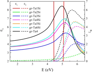
Previously in Tables 3.6 and 3.8 was evident that the models for the Ta1Si and gr-Ta2Si do not give physically reliable results. The problem with the models of gr-Ta1Si and gr-Ta2Si is shown in Figure 3.8 and in Table H.2. There is a huge discrepancy between this two models and the other models. Despite the attempts, better models were not achieved.
Figure 3.8: Real and imaginary part of the dielectric function of the samples.
With the representation ofε1andε2it is possible to see that with higher concentration
of Ta2O5the peaks become more intense. This is also perceptible in Table H.2 where the
parameterA1increases. This means that the films become denser [17, 47]. The parameter
C1also increases with the concentration of Ta2O5 which reveals that the films have a
decrease of short-range order with the increase of the rf power in the Ta2O5target [17,
47] which contradicts the reported results [24]. However, the decrease ofEg with the
increase of the Ta2O5concentration is in agreement with the literature [24]. It is also
possible to conclude that all Ta2O5films are amorphous, because the increase of theε2
with the photon energy is not abrupt [26].
3 . 2 . TA S I O SA M P L E S
In summary, with this set of samples it was possible to conclude that the density, Ta2O5
composition and growth rate increase with the rf power in the Ta2O5target at the same
time as the short-range order decreases. Once again, the success of the implementation of XRR was demonstrated.
3.2.2 Dielectric layer (d-TaSiO samples)
After the characterization of the gr-TaSiO samples to calculate the growth rate, the charac-terization of the d-TaSiO samples will be presented. The first part of this characcharac-terization is the analysis of the thickness, roughness and composition of the film and of the na-tive oxide. The second part to be shown is the electric characterization of the films as a dielectric layer in a MIS structure.
In this section the thicknesses were obtained by two techniques: SE and RBS. The results are presented in Table 3.9. The deposition time used to fabricate these samples was based on the growth rate calculated using the thicknesses obtained by profilometry (Table 3.7). With the exception of the sample d-Ta3Si, all samples have a thickness close to the desired 250 nm. Besides that, as have been noticed, the results for both techniques are very close to each other. This agreement can lead us to two other conclusions.
Table 3.9: Thicknesses obtained by SE and RBS.
Sample
Film thickness (Å) Film thickness(atomscm−2)
SE RBS RBS
d-Ta2Si 2395 ± 14 (236 ± 12)×10 1668 d-Ta3Si 2049 ± 7 (204 ± 11)×10 1495 d-Ta4Si 2425 ± 8 (241 ± 13)×10 1796 d-Ta5Si 2311 ± 10 (228 ± 12)×10 1712 d-Ta6Si 2550 ± 11 (256 ± 13)×10 1923 d-Ta4 2520 ± 13 (237 ± 12)×10 1855
First it is important to take in mind that in order to calculate the thicknesses from the RBS results it was assumed the mass density of the SiO2and Ta2O5of 2.2 and 8.2 gcm−3,
respectively. Not only that, but it is fundamental to understand that the fits were done assuming that the components of the films were Ta2O5, SiO2and Ar (although Ar is not
used to calculate the thicknesses). This means that the results presented are the results of the fit with the molecules and not the fit with the elements (Appendix G).
Therefore, if the results of both techniques are so similar with these assumptions, it means that the assumed stoichiometry may be close to the real stoichiometry of the com-ponents of the films and that the comcom-ponents have a density close to the bulk densities.
C H A P T E R 3 . R E S U LT S A N D D I S C U S S I O N
RBS and SE is shown in Table 3.10. The results are the expected ones: with the increase of the rf power in the Ta2O5target the concentrations of Ta2O5and Ar increase.
Table 3.10: Composition in molecular % obtained by RBS and SE data analysis.
Sample
RBS Normalized RBS SE
Ta2O5(%) SiO2(%) Ar (%) Ta2O5(%) Ta2O5(%)
d-Ta2Si 37.5 59.1 3.4 38.8 40.6
d-Ta3Si 57.6 38.6 3.8 59.9 56.4
d-Ta4Si 65.7 30.0 4.3 68.7 60.5
d-Ta5Si 70.6 25.0 4.5 73.8 61.5
d-Ta6Si 71.7 24.0 4.3 74.9 66.3
d-Ta4 94.5 - 5.5 100
-The results were the expected because on one hand in the RBS data (Figure 3.9) the peak of the Ta also increases with the increase of the rf power. This means that the quantity of Ta is also increasing. On the other hand, the trapping of rare gases in sputtering is proportional to the atomic mass of the targets. Since Ta2O5 has a higher
atomic mass than SiO2, with the increase of the molecular % of Ta2O5, more Ar atoms
are trapped in the deposited film [49].
Figure 3.9: RBS spectra from all samples with the respective fits in red.
Also in Table 3.10 it is compared the molecular % of the Ta2O5obtained by RBS and
SE. In this comparison it was used a normalised concentration in the RBS data analysis. The normalised concentration only takes into account the concentration of Ta2O5 and
SiO2. This was used because not only it is not possible to calculate the thickness with
films that have gases in its constituents, but also because in the SE data analysis presented here, Ar were not considered as well.
3 . 2 . TA S I O SA M P L E S
The molecular % of the Ta2O5presented for the SE data analysis was calculated too.
Using a different model (Figure E.3), the volumetric concentration of the Ta2O5was fitted.
The mass densities were assumed to calculate the molecular %. Knowing that RBS gives more viable results, one can conclude that it is possible to obtain a concentration with SE, but the result can only be used to give an idea of the concentrations and cannot be assumed as a certain result. This is the case because in these analyses the concentration of Ta2O5and the Tauc-Lorentz model of Ta2O5were fitted at the same time.
Besides the thickness and composition, SE give more information, namely the thick-ness of the silicon oxide and the roughthick-ness of the Ta2O5films. However, as one can see in
the table below (Table 3.11), the models obtained by SE revealed to be not very accurate for these two parameters. On one hand, the values of the native oxide thickness are not similar between samples. On the other hand, the roughness could not be obtained for two samples and is not consistent in the others. Nevertheless, it seems that the thickness of the Ta2O5was not affected by these problems. Nevertheless, the parameters of the
Tauc-Lorentz models can give more information (Figure 3.10 and Table H.3)
Table 3.11: Thicknesses of the native oxide and roughnesses of the Ta2O5.
Sample SiO2
thickness (Å)
Ta2O5
roughness (Å)
d-Ta2Si 14 ± 8 NS
d-Ta3Si 22 ± 3 NS
d-Ta4Si 9 ± 3 5 ± 2
d-Ta5Si 16 ± 4 8 ± 2
d-Ta6Si 18 ± 4 4 ± 2
d-Ta4 21 ± 5 11 ± 2
C H A P T E R 3 . R E S U LT S A N D D I S C U S S I O N
To conclude the first part of the characterization of the d-TaSiO samples one may look to the results of the Tauc-Lorentz models. Those results are in line with the results of the gr-TaSiO samples: the films become denser and have a decrease of short-range order with the increase of the rf power in the Ta2O5target and all films are amorphous. This is
shown in both Figure 3.10 and Table H.3.
The second part of this characterization consisted in the electrical characterization of MIS structures using the d-TaSiO films as dielectric layers. Therefore, the capacitance was measured as a function of the frequency (capacitance characteristic) and voltage.
The objective of the study of these films was to use them as the dielectric layer in transistors. So, the possibility of measuring these films in high frequency was desired. However, as one can see in Figure 3.11 for frequencies higher than 100 kHz the capaci-tance starts to increase. This effect is due to the high impedance of the cables. Because of
that, the remain electrical tests were performed using a frequency of 100 kHz.
Figure 3.11: Electrical measurements of the d-TaSiO samples.
To know the dielectric constant of the films the capacitance was measured in function of the applied potential, as shown in the figure above. Knowing that the contacts’ size was 494 µm×494 µm, using the thicknesses obtained by SE (Table 3.9) and with the maximum capacitance of the films (Figure 3.11), the dielectric constant was calculated.
To get a better understanding of the calculated dielectric constants, the results are presented in Figure 3.12. As it is possible to see there, the dielectric function increases with the increase of molecular % of Ta2O5 in the films (caused by the increase of the
rf power in the Ta2O5 target). The results are in agreement with the expected ones.
The dielectric constants of SiO2 and amorphous Ta2O5 are 3.9 [50] and 22-25 [51, 52],
respectively. So, with the increase of the molecular % of Ta2O5, the dielectric constant of
the films gets closer to the dielectric constant of the amorphous Ta2O5.
3 . 3 . Z T O SA M P L E S
Figure 3.12: Dielectric constants obtained from the electrical measurements.
In conclusion, with these sets of samples of films with different mixtures of Ta2O5and
SiO2was possible to see that the films become denser and have a decrease of short-range
order with the increase of the rf power in the Ta2O5. Is was also possible to conclude that
with the increase of the rf power the molecular % of Ta2O5also increased which lead to
an increase of the dielectric constant.
3.3 ZTO samples
The final set of samples characterized was a set of ZTO films grown by rf sputtering. These samples were fabricated at the same time as the samples used by C. Fernandes et al.as the dielectric layer in TFTs for flexible electronics [34]. Here the objective was to understand the role of some fabrication parameters, namely the rf power in the ZTO target and the flow of O2and H2. The nomenclature used is presented in Table 3.12.
Table 3.12: Samples nomenclature used in function of the fabrication parameters.
Sample Rf power (Wcm−2)
H2flow
(sccm)
O2flow
(sccm)
P1-H1-O2 1 0 5.36
P1-H2-O2 1 0.5 5.36
P1-H3-O2 1 1 5.36
P2-H1-O1 2 0 1.78
P2-H1-O2 2 0 5.36
P2-H2-O2 2 0.5 5.36
P2-H3-O2 2 1 5.36
P2-H1-O3 2 0 10.72
P2-H2-O3 2 0.5 10.72
C H A P T E R 3 . R E S U LT S A N D D I S C U S S I O N
In line with the other sections of this work, the XRR data was analysed using the procedure presented in Appendix B and once again the fit of the SLD of the native oxide and of the silicon were not viable. To solve this problem the assumed values of the SLD used for the Si and SiO2 were 18.886×10⁻⁶ and 20.124×10⁻⁶Å−2, respectively. These values are the theoretical ones. A more detailed explanation of these problem can be found in Appendix F.
Nevertheless, and as in the previous sections, very good fits of the measures XRR data was obtained. In Figure 3.13 the real data and the fit of a sample is presented. This is a representative example because for the remain samples the quality of the fits was as good as the fit of this sample.
Figure 3.13: Real data and XRR fit of the sample P1-O2-H1.
To study the correlation of the thicknesses determined by both techniques, a compari-son was made and it is presented in Figure 3.14. The result obtained with this comparicompari-son is similar to other results presented in this work as well as to the results reported in the literature [11, 44–46]. In other words, the result of the linear fit was a slope close to 1 and the interception is different than 0. As in the previous section, an explanation for the
interception being different than 0 was not found.
3 . 3 . Z T O SA M P L E S
Figure 3.14: Comparison between thicknesses obtained from XRR and SE.
3.3.1 Influence of the rf power
The first parameter studied was the rf power in the ZTO target. Two different rf powers
were tested: 1 Wcm−2 (P1) and 2 Wcm−2 (P2). Besides the change in the rf powers,
the deposition time was also changed. In the samples where 1 Wcm−2 was used, the
deposition time was 20 min. The deposition time of the samples where 2 Wcm−2 was
used was 5 min. This means that using twice the rf power, the time used was a quarter. With this, half of the thickness was expected for the P2-samples compared to the P1-samples and that was the result, as one can see in Table 3.13. Besides that, it is noticeable that both techniques are in very good agreement.
Table 3.13: Results from XRR and SE data analyses of the samples with different target rf power using Si and SiO2SLD values of 18.886×10⁻⁶and 20.124×10⁻⁶Å−2, respectively.
Sample
Film thickness (Å)
Film SLD (10−6Å−2)
Film roughness (Å)
SE XRR XRR XRR
P1-O2-H1 299 ± 2 305 ± 5 44 ± 3 8 ± 2
P2-O2-H1 157 ± 2 161.1 ± 0.6 47 ± 3 6.4 ± 0.4
P1-O2-H2 311 ± 11 330 ± 3 45 ± 3 8 ± 2
P2-O2-H2 172 ± 2 161.5 ± 0.4 47 ± 3 6.0 ± 0.4
P1-O2-H3 306 ± 2 309 ± 3 44 ± 3 9 ± 2
P2-O2-H3 165 ± 2 156.0 ± 0.5 49 ± 3 6.4 ± 0.4
The differences between P1- and samples are not just in the thicknesses.
C H A P T E R 3 . R E S U LT S A N D D I S C U S S I O N
are thinner. To test this hypothesis, samples with similar thicknesses should be fabricated using different rf powers. Besides the roughness, the SLD also changes. The SLD increases
with the increase of the rf power. Although the change is slight for the given uncertainties, it is possible to conclude that the density of the films increases with the increase of the rf power (supported by the increase ofA1with the rf power shown in Table H.4).
The increase of the density is also confirmed by SE because as shown in Table H.4 the parameter A1 is also higher for P2-samples [17, 47]. Looking at the Tauc-Lorentz
parameters for this sample is also possible to see an increase of the parametersE1 and C1. So, despite being denser, the sample also has a lower short-range order [17, 47]. With
SE one can also conclude that the samples are amorphous, because as shown in Figure I.1 theε2does not present an abrupt change with the photon energy [26].
3.3.2 Influence of the H2flow
The second parameter studied was the H2 flow during the rf sputtering. To test the
influence of this parameter, samples with three different flows were prepared. Some
samples were fabricated without H2 flow (H1), some with a flow of 0.5 sccm (H2) and
others with a flow of 1 sccm (H3).
Starting with the thickness, one can see that the thicknesses are higher in the H2-samples. This may indicate that the use of H2 flow in the fabrication of the samples
can lead to higher thicknesses. Nevertheless, a critical point of H2flow may exist as the
thicknesses are lower in the H3-samples than the H2-samples. More tests with more values of H2 flow should be performed to obtain better conclusions. Besides that, it
seems that the SLD increases with the H2flow but when one takes in consideration the
associated uncertainty, that conclusion is not very clear.
Table 3.14: Results from XRR and SE data analyses of the samples with different H2flow using Si and SiO2SLD values of 18.886×10⁻⁶and 20.124×10⁻⁶Å−2, respectively.
Sample
Film thickness (Å)
Film SLD (10−6Å−2)
Film roughness (Å)
SE XRR XRR XRR
P1-O2-H1 299 ± 2 305 ± 5 44 ± 3 8 ± 2
P1-O2-H2 311 ± 11 330 ± 3 45 ± 3 8 ± 2
P1-O2-H3 306 ± 2 309 ± 3 44 ± 3 9 ± 2
P2-O2-H1 157 ± 2 161.1 ± 0.6 47 ± 3 6.4 ± 0.4 P2-O2-H2 172 ± 2 161.5 ± 0.4 47 ± 3 6.0 ± 0.4 P2-O2-H3 165 ± 2 156.0 ± 0.5 49 ± 3 6.4 ± 0.4 P2-O3-H1 165 ± 2 152.2 ± 0.9 43 ± 3 6.3 ± 0.9
P2-O3-H2 152 ± 1 150 ± 1 44 ± 3 6 ± 1
P2-O3-H3 143 ± 2 139.5 ± 0.8 46 ± 4 6.0 ± 0.7
![Figure 1.3: Representation of the components of the electric field of a light beam [12].](https://thumb-eu.123doks.com/thumbv2/123dok_br/16699277.743940/27.892.172.733.574.795/figure-representation-components-electric-field-light-beam.webp)