Brazilian Microwave and Optoelectronics Society-SBMO received 23 Jul 2018; for review 26 Jul 2018; accepted 08 Nov 2018
Brazilian Society of Electromagnetism-SBMag © 2018 SBMO/SBMag ISSN 2179-1074
Abstract - A characterization technique, including a mathematical model involving extensive computational resources, is introduced to study the behavior of an electro-optical space switch based on semiconductor optical amplifier (SOA). The model encompasses the precise emulation of device nonlinearities and its transient performance, allowing the characterization of its transient response. The calibration process includes the evaluation of parasites from the SOA connection, mounting and encapsulation, and parameter extraction of the active cavity. The numerical results are compared to experimental data for various operational conditions, with close similarities. The characterization technique can be adapted for other electro-optical devices, such as directed-modulated lasers, amplitude modulators and electro-optical switches.
Index Terms—Electro-optical devices, electro-optic switches, equivalent circuit, semiconductor optical amplifier, simulation.
I. INTRODUCTION
The exponential increase in fiber optic networks’ capacity claimed by new applications such as the
Internet of Things, cloud computing, and streaming services calls for novel scientific approaches and
low cost technological innovations to fulfill market demands. In this sense, all-optical networks are a
promising solution, avoiding the electronic bottlenecks of several optical-electrical-optical (O/E/O)
conversions, as well as its inherent latency [1]. In Data Centers (DCs) optical packet switching (OPS)
achieves latencies up to 25 ns, representing a clear improvement in comparison with the 90 ns
typically introduced by equivalent all-electrical switches [1]. Complementarily, all-optical
interconnects provide power consumption reduction [2], [3], cooling systems simplification and
effortless network expansion.
A promising device to achieve integration of complex components in all-optical networks is the
semiconductor optical amplifier (SOA). Its versatility permits several electro-optical functions such as
WDM amplification [4]]-[[6], wavelength conversion [7], [8], wavelength selection [9], wavelength
Computational Model and Parameter
Extraction of High Speed Semiconductor
Optical Amplifier Space Switches
T. Sutili¹, P. Rocha¹, Ernesto M. M. Barrientos1,2, A. C. Bordonalli1, C. M. Gallep3, and E. Conforti¹,
¹Department of Communications, School of Electrical and Computing Engineering, University of Campinas, Campinas-SP, Brazil
2São Paulo Federal Institute (IFSP), Guarulhos, SP, Brazil 3School of Technology, University of Campinas, Limeira-SP, Brazil
Brazilian Microwave and Optoelectronics Society-SBMO received 23 Jul 2018; for review 26 Jul 2018; accepted 08 Nov 2018
Brazilian Society of Electromagnetism-SBMag © 2018 SBMO/SBMag ISSN 2179-1074 routing [10], and carrier wavelength reusing [11], [12]. Furthermore, its integrability enables the
implementation of logic gates [13]-[15], optical adders and subtractors [16], memory modules [17],
optical buffers [18]]-[[20], optical demultiplexers [21], and wavelength selectors [22]. Through SOAs
nonlinear behavior, it is also possible to project all-optical regenerators for intensity modulated [23],
[24], phase encoded [25], [26], and coherent signals [27]. Furthermore, SOAs can perform optical
packet switching, allowing the construction of SOA-based OPS (M × N switches), which can
establish connections between ports in the order of few nanoseconds [28]. These devices take
advantage of the polarization insensitivity [29] and ultrafast transitions from off to on operational
states in SOA-based optical space switches [30], which is possible through the dynamic behavior of
electrical and optical carriers in the SOA active region [31]]-[[33]. In addition, SOA can
simultaneously amplify the switched carrier, compensating for switch insertion loss and improving the
optical link signal-to-noise ratio [34].
The study of SOA switching performance shows that the reduction of electrical parasites
(especially, capacitances and inductances due to packaging and microwave mounting) results in
further improvements in the device electro-optical response velocity and stability. However, there is a
trade-off between overshoots and rising times, being all linked to the electrical parasite fading [35].
One tool to evaluate the complex interaction between device parasites and its electro-optical
performance is the equivalent circuit-based numerical analysis, which confirmed that packaging
inductances and capacitances restrict the switching rise time and induce output power fluctuations
[36]. By employing the experimental system response modeling into the electrical equivalent circuit,
it is possible to extract important electro-optical parameters such as capacitances, inductances, and
resistances inherent to the SOA assembly (transmission and coupling lines, encapsulation, and
mounting).
Expanding this approach, the work here proposes the complete modeling of a nonlinear SOA,
including the simulation of its microwave parasitic elements and the inference of its constructive and
operational properties, which will greatly affect its dynamic performance. Through the comparison of
the model behavior and experimental results, it was possible to precisely extract meaningful
parameters related to SOA encapsulation, mounting, and architecture. This modeling approach can be
applied to any traveling wave SOA (or other electro-optical device), allowing for an analysis of its
particular characteristics and performance. Previous works showed that the direct experimental
evaluation of these SOA parameters can be challenging, supporting the importance of alternative
means to extract this information and emulate it into a precise computational model. In [37], the
electric SOA equivalent circuit was used to investigate the mitigation of inter-channel crosstalk by
assist light in a TOAD (Terahertz Optical Asymmetric Demultiplexer) switch. The methodology
Brazilian Microwave and Optoelectronics Society-SBMO received 23 Jul 2018; for review 26 Jul 2018; accepted 08 Nov 2018
Brazilian Society of Electromagnetism-SBMag © 2018 SBMO/SBMag ISSN 2179-1074 computational resources in conjunction with experimental references, permitting not only the device
modeling but also the analysis of its transient behavior and performance under several operational
conditions. As it will be further discussed in Section A, the approach allowed the determination of the
electrical microwave pulse signal that is actually injected into the SOA active region, considering
distortions caused by electric parasites [35]. By employing the obtained microwave signal as system
electrical input, as it will be presented in Section B, it is possible to model the device optical response
(i.e., the SOA optical gain and dynamic behavior, as a function of the injected bias current or the
optical input power) in relation to its operational and constructive parameters. In [38], the dynamic
SOA response for modulated optical signals up to 10 Gb/s was obtained by using a so called reservoir
model, which adapted parameters previously obtained from a steady-state response model presented
in [39]. The dynamic response modeling applied to SOA-based photonic processing, especially using
XGM (Cross-Gain Modulation), is presented in [40]. As a matter of fact, SOAs with different
characteristics (especially, composition and geometry), will present variations in their optical
responses. The results discussed in Section III show the dynamic behavior simulation of a practical
optical switch through the computational modelling technique here presented. As addressed in Section
IV, this can be a valuable tool to the complete performance characterization of photonic devices in
complex optical networks.
II. MATERIAL AND METHODS
The SOA dynamic modelling technique is based on two sequential procedures, covering the
inference of microwave parasites from the mounting and the device operational and constructive
parameter calibration. Firstly, the electrical switching pulse injected into the SOA active region is
determined by taking into consideration the transient oscillations induced by the SOA mounting. For
this purpose, the SOA experimental optical switching pulses were employed as reference to evaluate
each component in a electrical equivalent circuit calibrated through Simulink [41] simulation. In
particular, the nonlinear SOA model under analysis and used during the experimental validation is the
CIP-NL-OEC-1550, from now on referred to as CIP-NL. Next, the SOA electro-optical dynamic
behavior is adjusted employing the mentioned electrical switching pulses as input and, once again,
experimental results as reference. Through heuristic extraction employing numerical analysis, it was
possible to refine the default VPI [42] SOA model, extracting the devices operational parameters and
constructive characteristics and emulating its dynamic performance in experimental conditions.
A Equivalent Circuit Calibration (Simulink)
By taking advantage of the constructive similarities between SOAs and semiconductor lasers (as a
matter of fact, the first is basically the second with anti-reflective coatings in its active region facets),
Brazilian Microwave and Optoelectronics Society-SBMO received 23 Jul 2018; for review 26 Jul 2018; accepted 08 Nov 2018
Brazilian Society of Electromagnetism-SBMag © 2018 SBMO/SBMag ISSN 2179-1074 response. This approach was extensively exploited in previously works [44], [45], [33], resulting in
the extraction of approximate parameters from the characterized SOA. However, in those cases, the
fitting between simulated equivalent circuit and experimentally evaluated responses was performed
only on the frequency-domain, resulting in an inaccurate SOA behavior in time-domain simulations
[44]. Furthermore, the equivalent circuit component evaluation was carried out heuristically, resulting
in an extensive work to evaluate the complex interaction between all electrical elements. In general,
this methodology results in an incomplete characterization of SOA-based switch properties, as
evidenced by high-frequency oscillations in time-domain which do not follow the experimental
behavior [44]. The proposed methodology is constructed on a different approach that employ the
possibility of performing several equivalent circuit simulations directly in time-domain, where
electrical component values are varied until the output converges to the desired SOA behavior.
The electrical equivalent circuit is presented in Fig. 1 and contains tree different stages. The first
one, named “Coupling”, is related to microwave mounting and parasites elements derived from SOA. The second one, referred to as “Encapsulation”, is formed by parasitic elements associated with the
SOA chip encapsulation in a form factor suitable for commercial distribution. Finally, the third one,
called “SOA”, emulates the device itself, converting the input electrical microwave pulse in an equivalent optical signal output (proportional to the electrical current ieq). A more comprehensive
view of the equivalent circuit model is possible through the physical interpretation of each electrical
component. Regarding the SOA elements: CS is a SOA mounting parasitic element dependent on the
electrical current injected into the device; RS stands for a small-loss of the SOA input current in the
mounting; CSC represents the heterojunction space charge capacitance, emulating the electrical carrier
storage; CD is the diffusion capacitance, standing for the electrical carrier lifetime; RE is the
heterojunction effective resistance; LS is the SOA active region optical carrier storage; RS1 emulates
the SOA gain compression; and, RS2 represents the device spontaneous emission. However, the
electrical current injected into the SOA is previously degraded by the coupling and encapsulation
parasitic elements: TL stands for a transmission line intended to guide the microwave signal into the
SOA mounting; RC is a coupling resistor with matches the mounting input impedance to that of the
generator output; CA, LA, CB, and LB are coupling parasitic elements from the microwave connections;
CP, LP, and RP are parasitic elements linked with the SOA's chip enclosure in its commercial form
Brazilian Microwave and Optoelectronics Society-SBMO received 23 Jul 2018; for review 26 Jul 2018; accepted 08 Nov 2018
Brazilian Society of Electromagnetism-SBMag © 2018 SBMO/SBMag ISSN 2179-1074
Fig. 1: Equivalent circuit employed in the microwave mounting and SOA active region modelling.
Nevertheless, the SOA is an electro-optical component with inherently nonlinear behavior,
characteristic that is especially evident when operating with larger signals, as occurs in the switching
process. In this sense, it is impossible for a linear equivalent circuit, as the one proposed in Fig. 1, to
perfectly emulate the device dynamic behavior, particularly its transient oscillations after the pulse
rising edge. Due to the fundamental limitations of this approach, the equivalent circuit parameters
extraction in Simulink environment intended primarily to evaluate the electrical current that is
actually injected in the SOA heterojunction. An in-deeper modelling of the SOA itself is carried out in
the VPI environment, which has the tools required to carefully adjust the semiconductor constructive
and operational characteristics, as discussed in Section B. A better equivalent circuit could then be
achieved with nonlinear circuit elements, especially the ones corresponding to the SOA active region
emulation. One way to implement that is to adopt current dependent resistors and capacitors, which
could model with accuracy the SOA active region refractive index dependence with the device gain
and input optical power. Another solution could be the use of time-domain partial linearization of
switching pulses, which consist on analysing each pulse segment and considering different electric
elements values for each instant, thus matching specifically the SOA operational condition for drastic
output power transient oscillations.
Yet, the equivalent circuit was employed here only to approximate the parasitic degradation
impacting the electrical current injected into the SOA heterojunction, being appropriate to this
purpose. To approximate the equivalent circuit output current ieq with the actual device behavior, the
developed algorithm performs several simulations, adjusting the electrical components values in
increasing smaller ranges, getting progressively closer to the experimentally characterized optical
switching pulse employed as reference. As each optical component variation has an overall impact in
several switching pulse characteristics, it is crucial to constantly evaluate the similarities between the
simulated and experimental pulses. With this objective, several evaluation metrics were employed,
including pulse rise time, percentage overshoot, transient behavior, stabilization time, percentage
undershoot, and mean square error. After each interaction, the developed algorithm automatically
evaluates these performance metrics, comparing the circuit output electrical current ieq (which is
Brazilian Microwave and Optoelectronics Society-SBMO received 23 Jul 2018; for review 26 Jul 2018; accepted 08 Nov 2018
Brazilian Society of Electromagnetism-SBMag © 2018 SBMO/SBMag ISSN 2179-1074 these signals get closer time-domain shapes (evidenced by smaller errors in these metrics), the
algorithm saves the equivalent circuit electrical element values, using them as seeds for the next
iteration. If one interaction diverges from the expected experimental behavior, the correspondent
values are discarded. After several thousand iterations, a good approximation between the equivalent
circuit response and the experimental reference is achieved.
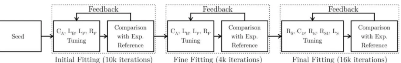
The steps followed by the Simulink algorithm are presented in the Fig. 2, showing the three
different calibration stages. Initially, the developed algorithm is fed with previously published values
for the CIP-NL equivalent circuit [46] as a seed. Aiming a first approximation, only are the
parameters with high impact in the switching pulse overall behavior (i.e., CA, LB, LP, and RP) adjusted
in a wide range. After a good initial match is achieved, these values are refined through their variation
in smaller steps. Next, a fine tuning of the electrical elements directly linked to the electro-optical
conversion (i.e., RS, CD, RE, RS1, and LS) is performed, allowing a final calibration involving all the
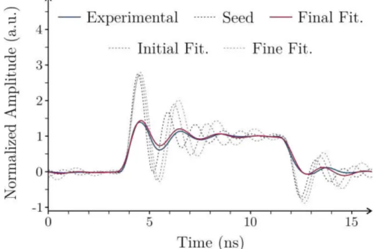
equivalent circuit electric elements. The results of this approximation and calibration process are
illustrated in Fig. 3, where it is possible to note closer approximations between the experimental
switching pulse and the equivalent circuit outputs in each stage of Fig. 2.
Figure 2: Block diagram with the Simulink steps for the equivalent circuit calibration process.
This calibration approach can be quantitatively evaluated through the metrics employed in the
developed algorithm, as presented in Table 1, which refers to the pulses in Fig. 3. However, as
evidenced by the pulses in this figure, the calibrated equivalent circuit in unable to emulates perfectly
the SOA transient behavior. In fact, this behavior is intrinsically linked to its active region
nonlinearities and coupled optical and electrical carriers, which cannot be simulated through a linear
electrical circuit. As previously discussed, this approach is limited to evaluate the mounting and
encapsulation parasitic element impact on the device performance. Therefore, the calibrated
equivalent circuit was employed mainly to appraise the electrical current injected into the SOA
Brazilian Microwave and Optoelectronics Society-SBMO received 23 Jul 2018; for review 26 Jul 2018; accepted 08 Nov 2018
Brazilian Society of Electromagnetism-SBMag © 2018 SBMO/SBMag ISSN 2179-1074
Fig. 3: Time domain switching pulse showing a comparison between experimental and equivalent circuit calibration results for increasingly refinement as a function of the evaluation metrics. The reference experimental pulse was obtained through the switching of a nonlinear SOA (CIP-NL) with 100 mA bias, 3 V switching step, and 3 V PISIC pre-impulse.
TABLE I.EQUIVALENT CIRCUIT CALIBRATION METRICS
Evaluation Metric Seed Circuit Calibrated Circuit
Rise Time Error 128.12 ps 101.56 ps Overshoot Error 133.67 % 4.72 % Transient Frequency Error 314.12 ps 23.41 ps
Stabilization Time Error 107.78 ps 31.32 ps Undershoot Error Mean 63.84 % 0.41%
Mean Square Error 1171.49 24.88
B Dynamic Response Calibration (VPI)
The SOA dynamic response calibration was performed following the technique proposed in [47]
and detailed in Section C. Through this approach, it was possible to precisely tune the SOA static
optical gain in the VPI environment [42] as a function of its bias current and optical input power. This
first SOA response approximation was then expanded considering its dynamic behavior when
switching pulses, as the ones evaluated in Section A via Simulink environment [41], were summed up
with the device bias current, as discussed in Section D.
C Static Gain Calibration
Parameters such as the SOA active region length, width, and thickness can affect the electro-optical
switching behavior, since the SOA optical gain is inherently dependent on them. Unfortunately, these
parameters are seldom provided by manufacturers, and its experimental extraction is complex.
Usually, length and width can be measured using scanning electron microscopy on an open device,
and length can be obtained by analysing residual Fabry-Perot modes [48]. However, these parameters,
among several others, as showed in Table 2, can be obtained through heuristic extraction, employing
Brazilian Microwave and Optoelectronics Society-SBMO received 23 Jul 2018; for review 26 Jul 2018; accepted 08 Nov 2018
Brazilian Society of Electromagnetism-SBMag © 2018 SBMO/SBMag ISSN 2179-1074
TABLE II.PARAMETERS FOR SOA MODEL.
Parameter Default Static Dynamic
Active Region Type MQW MQW MQW Width of Active Region 2.5 µm 650 µm 650 µm
Cavity Length 2 mm 2 mm 2 mm Thickness of Active Region 40 nm 200 nm 200 nm Thickness of the SCH Region 210 nm 210 nm
Injection Efficiency Coefficient (I )
1.00 0.85 0.85 Internal Losses Cefficient (ILC) 3000 m-1 2500 m-1 2500 m-1 Internal Loss Carrier Dependence
(ILCD)
1∙10-23
m2 1.1∙10-21 m2
MQW Confinement Factor 0.07 0.26 0.26 SCH Confinement Factor 0.56 0.56 0.56 Optical Coupling Efficiency (OCE) 1.00 0.60 0.60
Linear Gain Coefficient (Gcoeff) 3∙10-20 m2 4.63∙10-20 m2 4.63∙10-20 m2
Carrier Density Reference Gain Shape (N )
2∙1024
m-3 1∙1024 m-3 1∙1024 m-3
Carrier Density in the Transparency (CDT)
1.5∙1024
m-3 0.91∙1024 m-3 0.911∙1024 m-3 Initial Carrier Density (ICD) 1∙1024 m-3 1∙1023 m-3 1∙1023 m-3 Nonlinear Gain Coefficient (ε) 1∙10-23 m3 1∙10-21 m3 2.9∙10-21 m3 Linear Recombination (Arecomb) 1∙107 s-1 5.5∙108 s-1 5.5∙108 s-1
Bimolecular Recombination (B) (B )
1∙10-16
m3∙s-1 2∙10-16 m3∙s-1 2∙10-17 m3∙s-1 Auger recombination (Crecomb) 1.3∙10
-41
m6∙s-1 0.5∙10-41 m6∙s-1 0.5∙10-41 m6∙s-1 Carrier Capture Time Constant
(Capture Time)
7∙10-11
s 7∙10-12 s 7∙10-12 s Carrier Escape Time Constant
(Escape Time)
14∙10-11
s 14∙10-11 s 14∙10-11 s
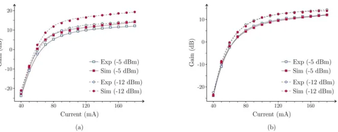
This approach was experimentally implemented by using the setup presented in Fig. 4, with the
electrical current injected into the SOA heterojunction being formed only by the direct current bias
component (i.e., switching pulses equal to zero). The laser was in continuous wave (CW) mode at
1550 nm and an optical isolator in its output prevented optical backward propagation. The optical
carrier was then amplified by the SOA with its output acquired by an optical spectrum analyser
(OSA). By changing the SOA bias current (from 40 mA up to 180 mA) and input optical power (from
-25 dBm up to 8 dBm), it was possible to characterize the SOA static optical gain behavior, which
was the reference for the VPI model calibration, as presented in Fig. 5 and 6.
The VPI SOA model uses the transmission-line matrix (TLM) method to emulate the propagation
of light across the device active region. Its static calibration begins with the SOA active region length
experimental evaluation via [48], which is then set in the VPI model. Next, the parameters listed in
Table 2 were individually tuned from its default values, analysing the impact of their variation on the
simulated curves of optical gain versus bias current and versus input optical power. ‘Default’ are
values preconfigured for a standard SOA in the VPI software and that were used as start profile for
the calibration technique presented in [47]. The SOA active region’s optical confinement factor, width
and thickness are parameters of greater interest and impact on the overall static behavior and, then,
firstly analysed. The relationship among these three parameters also determines the saturation power
of the SOA output [40]. To analyse the joint relationship among them, a simultaneous scan of the
Brazilian Microwave and Optoelectronics Society-SBMO received 23 Jul 2018; for review 26 Jul 2018; accepted 08 Nov 2018
Brazilian Society of Electromagnetism-SBMag © 2018 SBMO/SBMag ISSN 2179-1074 5(a). Following, parameters with less impact were individually adjusted, allowing fine tuning of the
SOA saturation and gain, as presented in Fig. 5(b). A final model calibration was performed through
the analysis of the SOA optical gain as a function of its input optical power, as presented in Fig. 6.
The calibrated parameters, which resulted in the behavior of Fig. 5(b) and Fig. 6 and are presented in
Table 2 in the “Static” column, are then used in the SOA rate equations solving and applied to the wave equations, which are used to model the optical signal propagation within the active region of the
device. The solutions of these equations are obtained numerically by the TLM method [49].
Fig. 4: Experimental setup for the SOA static gain characterization employed as reference for the VPI model calibration.
Brazilian Microwave and Optoelectronics Society-SBMO received 23 Jul 2018; for review 26 Jul 2018; accepted 08 Nov 2018
Brazilian Society of Electromagnetism-SBMag © 2018 SBMO/SBMag ISSN 2179-1074
Figure 6: Gain versus input optical power for simulated and experimental data: (a) SOA bias current equal to 40 mA, 60 mA, and 100 mA; (b) SOA bias current equal to 150 mA and 180 mA.
D Dynamic response calibration
The static gain calibration performed in the previous section does not necessarily describes the SOA
dynamic behavior when operating as an electro-optical switch. To precisely evaluate the influence of
each SOA model parameter in its dynamic operation, it is fundamental to realize the calibration
employing experimental data for time-domain switching pulses as reference, such as the one
presented in Fig. 3. However, as the VPI model does not include the SOA microwave mounting
responsible for injecting the switching pulses into the SOA, the equivalent circuit of Section A was
employed to evaluate the impact of the SOA encapsulation parasitic elements over the device overall
performance. In this sense, the setup of Fig. 4 was used with the electrical current injected into the
SOA being the sum of its bias and PISIC [50] switching pulses evaluated via the Simulink equivalent
circuit. From the SOA VPI model parameters calibrated in the previously section, additional tuning
was heuristically performed to approximate the simulated optical pulses to the experimental ones. An
initial calibration was performed by considering the SOA operating with a 100 mA bias current plus
an alternate switching pulse formed by a 3 V step without pre-impulse (directly applied to the SOA
using a 47 resistor in series with the SOA input impedance). After that, the resulting model was
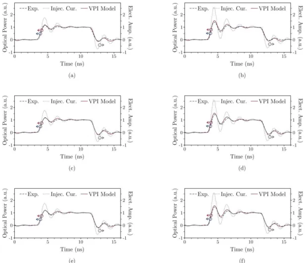
evaluated for the SOA operating under several conditions (bias current from 100 to 200 mA, step
amplitude from 1 to 3 V, and 0:64 ns pre-impulse from 0 to 3 V), as presented in Fig. 7. The obtained
calibrated parameters to accurately model the SOA dynamic behavior are presented in the “Dynamic”
column of Table 2.
III. RESULTS AND DISCUSSIONS
The CIP-NL modelling in the VPI environment can be verified by the time domain optical pulses
presented in Fig. 7 and by the evaluation metrics of Table 3, which describes quantitatively the SOA
Brazilian Microwave and Optoelectronics Society-SBMO received 23 Jul 2018; for review 26 Jul 2018; accepted 08 Nov 2018
Brazilian Society of Electromagnetism-SBMag © 2018 SBMO/SBMag ISSN 2179-1074 is possible to note in Fig. 7 that, by comparing to the SOA switching current injected into the SOA
heterojunction (previously evaluated through the Simulink equivalent circuit calibration), the VPI
model was able to approximately emulate the SOA complex dynamic between optical and electrical
carriers in its active region, matching the SOA transient behaviour, both regarding the oscillation
amplitude and, more important, frequency. As the SOA oscillations are directly linked to the coupled
dependence between carrier density and refraction index in its cavity, small variations on the model
calibration can lead to a significant impact in this complex simulation. Furthermore, each switching
pulse presented in Fig. 7 represents the SOA operating under different conditions, including variations
in its bias current, switching step amplitude, and PISIC pre-impulse amplitude. Each one of these
operational parameters has a significant influence in the SOA dynamic behavior and is directly linked
with its optical gain and nonlinear effects, proving that the VPI model became able to accurately
emulate the actual SOA performance in real operational conditions.
Brazilian Microwave and Optoelectronics Society-SBMO received 23 Jul 2018; for review 26 Jul 2018; accepted 08 Nov 2018
Brazilian Society of Electromagnetism-SBMag © 2018 SBMO/SBMag ISSN 2179-1074 A more quantitatively analysis is possible in Table 3, where the most important switching metrics
(i.e., rise time, overshoot, and stabilization time) are compared between the experimental reference
and the simulated VPI model. Note that the VPI model has a better correspondence with the
experimental pulses when operating in a intermediary bias current. In this region, the SOA operates
away from its deep nonlinear behavior. However, in all cases the errors in the evaluated metrics are
relatively low in comparison with the experimental references absolute values, validating the model
technique here proposed.
TABLE III.COMPARISON BETWEEN THE CALIBRATED VPISOA MODEL AND THE EXPERIMENTAL REFERENCES.
SOA Bias Current Switching Step Amplitude PISIC Pre-impulse Amplitude
Rise Time Overshoot Stabilization Time
Exp. Ref. Model Error Exp. Ref. Model Error Exp. Ref. Model Error
100 mA 2.00 V 0.00 V 560.62 ps 8.6 % 19.11 % 3.31 % 5.48 ns 60.94 ps 100 mA 3.00 V 3.00 V 401.32 ps 16.74 % 39.07 % 12.43 % 5.42 ns 92.19 ps 150 mA 2.00 V 0.00 V 621.88 ps 2.26 % 19.57 % 2.48 % 5.54 ns 7.81 ps 150 mA 3.00 V 3.00 V 443.75 ps 3.87 % 44.03 % 10.97 % 5.51 ns 7.92 ps 200 mA 2.00 V 0.00 V 629.29 ps 3.23 % 20.77 % 1.29 % 5.54 ns 1.57 ps 200 mA 3.00 V 3.00 V 431.25 ps 2.17 % 47.04 % 10.11 % 5.48 ns 10.01 ps
IV. CONCLUSION
The SOA is a promising electro-optical component, able to amplify, switch, regenerate, and route
an optical carrier. Yet, several of these applications are influenced or based on its highly nonlinear
behavior, which demands a careful device characterization and modelling to adequate its operation to
the desired application requirements. As the SOA performance is intrinsically dependent with its
complex active region carrier dynamics, each of its constructive and mounting parameters have a
significant impact on the model accuracy, turning the default model available in simulation softwares
unsuitable for the evaluation of the device impact on sophisticated optical networks.
The work here presented proposes a modeling technique capable of systematically predicting the
electrical current injected into the SOA heterojunction, considering the overall degradation imposed
by parasitic elements from the device mounting and encapsulation, by using an automated calibration
of an electrical equivalent circuit. Although this approach is capable of providing an initial good
approximation for the SOA optical output, the precise emulation of its nonlinear behavior demands a
more complex model to evaluate SOA active region carrier dynamics and its influence in the SOA
refractive index. To do that, the SOA injected current estimated by the equivalent circuit is employed
as the input electrical signal for the SOA VPI default model, which in turn is carefully tuned to
precisely emulate the SOA electro-optical performance, including its transient behavior. The results
showed a good approximation between the calibrated VPI model and the experimental reference,
Brazilian Microwave and Optoelectronics Society-SBMO received 23 Jul 2018; for review 26 Jul 2018; accepted 08 Nov 2018
Brazilian Society of Electromagnetism-SBMag © 2018 SBMO/SBMag ISSN 2179-1074 proposed here, can be crucial during the design of sophisticated devices and its application on
complex and efficient optical networks.
ACKNOWLEDGMENT
The authors would like to thank Prof. Dr. Adriano L. Toazza, Dr. Napoleão S. Ribeiro, and Dr. Rafael C. Figueiredo for their contributions to previously stages of this work. This work was supported in part by the Brazilian agencies São Paulo Research Foundation (FAPESP – grants 2017/20121-8, 2015/50063-4, 2015/24517-8, and 2007/56024-4) and National Council for Scientific and Technological Development (CNPq – grants 301409/2017-0, 159388/2017-1, 400129/2017-5, 402923/2016-2, and 301420/2015-7.
REFERENCES
[1] H. Meyer, J. C. Sancho, M. Mrdakovic, W. Miao, N. Calabretta, Optical packet switching in HPC: An analysis of applications performance, Future Generation Computer Systems doi:10.1016/j.future.2017.02.041.
[2] B. D. Feris, P. Gravey, P. Morel, M. L. Moulinard, M. Morvan, A. Sharaiha, Dimensioning of 112G optical-packet- switching-based interconnects for energy-efficient data centers, IEEE/OSA Journal of Optical Communications and Networking 9 (4) (2017) B124–B136. doi:10.1364/JOCN.9.00B124.
[3] S. Ni, B. Wu, Y. Liu, Characteristics of silicon-based Sagnac optical switches using magneto-optical micro-ring array, Fiber and Integrated Optics 37 (1) (2018) 12–20. doi:10.1080/01468030.2017.1423135.
[4] J. Renaudier, A. C. Meseguer, A. Ghazisaeidi, P. Tran, R. R. Muller, Brenot, A. Verdier, F. Blache, K. Mekhazni, B. Duval, H. Debregeas, M. Achouche, A. Boutin, F. Morin, L. Letteron, N. Fontaine, Y. Frignac, G. Charlet, First 100-nm continuous-band WDM transmission system with 115Tb/s transport over 100km using novel ultra-wideband semiconductor optical amplifiers, in: Optical Communication, 2017. 43rd European Conference on, Vol. 1, 2017, pp. 1– 3.
[5] Y. M. Zhang, Y. Liu, Z. K. Zhang, Z. P. Zhao, Y. Tian, N. H. Zhu, Reconfigurable WDM-PON empowered by a low-cost 8-channel directly modulated laser module, Optoelectronics Letters 13 (6) (2017) 423–426. doi:10.1007/s11801-017-7159-6.
[6] C. Zhang, T. Ning, J. Li, C. Li, X. He, L. Pei, Simultaneous MMW generation and up-conversion for WDM-ROF systems based on FP laser, Optics & Laser Technology 84 (2016) 94 – 101. doi:10.1016/j.optlastec.2016. 05.010. [7] T. Durhuus, B. Mikkelsen, C. Joergensen, S. L. Danielsen, K. E. Stubkjaer, All-optical wavelength conversion by
semiconductor optical amplifiers, Journal of Lightwave Technology 14 (6) (1996) 942–954. doi: 10.1109/50.511594. [8] F. Saadaoui, M. Fathallah, A. M. Ragheb, M. I. Memon, H. Fathallah, S. A. Alshebeili, Optimizing OSSB generation
using semiconductor optical amplifier (SOA) for 5G millimeter wave switching, IEEE Access 5 (2017) 6715–6723. doi:10.1109/ACCESS.2017.2683064.
[9] Z. Shen, L. Wang, X. Wang, Y. Cao, X. Feng, B. ou Guan, Tunable dual wavelength single-longitudinal-mode fiber laser based on spectral narrow-ing effect in a nonlinear semiconductor optical amplifier, Optics & Laser Technology 94 (2017) 72 – 76. doi:10.1016/j.optlastec.2017.03.020.
[10]X. Zheng, O. Raz, N. Calabretta, D. Zhao, R. Lu, Y. Liu, Multiport InP monolithically integrated all-optical wavelength router, Optics Letters 41 (16) (2016) 3892–3895. doi:10.1364/OL.41.003892.
[11]A. Chiuchiarelli, C. M. Gallep, E. Conforti, Fabry Perot laser-based optical switch for multicast transmission in bidirectional optical access networks, Microwave and Optical Technology Letters 58 (6) (2016) 1466–1469. doi: 10.1002/mop.29823.
[12]N. S. Ribeiro, C. M. Gallep, E. Conforti, Semiconductor optical amplifier cavity length impact over data erasing/rewriting, Microwave and Optical Technology Letters 55 (5) (2013) 998–1001. doi:10.1002/mop.27496. [13]A. Kotb, K. E. Zoiros, Performance analysis of all-optical XOR gate with photonic crystal semiconductor optical
amplifier-assisted MachZehnder interferometer at 160 Gb/s, Optics Communications 402 (2017) 511–517. doi:10.1016/j.optcom.2017.06.050.
[14]E. Dimitriadou, K. Zoiros, Proposal for ultrafast all-optical XNOR gate using single quantum-dot semiconductor optical amplifier-based Mach Zehnder interferometer, Optics & Laser Technology 45 (2013) 79 – 88. doi: 10.1016/j.optlastec.2012.07.024.
Brazilian Microwave and Optoelectronics Society-SBMO received 23 Jul 2018; for review 26 Jul 2018; accepted 08 Nov 2018
Brazilian Society of Electromagnetism-SBMag © 2018 SBMO/SBMag ISSN 2179-1074
[16]S. Mandal, D. Mandal, M. K. Mandal, S. K. Garai, Design of optical quaternary adder and subtractor using polarization switching, Journal of Optics. doi:10.1007/s12596-018-0460-3.
[17]D. Brunina, D. Liu, K. Bergman, An energy-efficient optically connected memory module for hybrid packet- and circuit-switched optical networks, IEEE Journal of Selected Topics in Quantum Electronics 19 (2). doi: 10.1109/JSTQE.2012.2224096.
[18]T. Tanemura, I. M. Soganci, T. Oyama, T. Ohyama, S. Mino, K. A. Williams, N. Calabretta, H. J. S. Dorren, Y. Nakano, Large-capacity compact optical buffer based on InP integrated phased-array switch and coiled fiber delay lines, Journal of Lightwave Technology 29 (4) (2011) 396–402. doi:10.1109/JLT.2010.2102338.
[19]G. Berrettini, G. Meloni, L. Poti, A. Bogoni, All-optical variable buffer based on semiconductor optical amplifier, IEEE Journal of Quantum Electronics 47 (4) (2011) 510–516. doi:10.1109/JQE.2010.2092752.
[20]W. Yongjun, X. Xiangjun, S. Chao, Multichannel packets buffering in cascaded double-loop optical buffer based on the pure phase switching of gain-transparent semiconductor optical amplifier, Optical Engineering 53. doi:10.1117/1.OE.53.1.016101.
[21]M. Matsuura, F. Gomez-Agis, N. Calabretta, O. Raz, H. J. S. Dorren, 320to-40-Gb/s optical demultiplexing using four-wave mixing in a quantum dot SOA, IEEE Photonics Technology Letters 24 (2) (2012) 101–103. doi: 10.1109/LPT.2011.2173672.
[22]R. Stabile, N. Calabretta, K. A. Williams, Switch-filter wavelength selector: simulation and experiment, IET Optoelectronics 8 (1) (2014) 1–10. doi: 10.1049/iet-opt.2013.0084.
[23]G. Chen, L. Xi, Y. Ma, L. Sun, X. Zhang, Regeneration of DQPSK signals using semiconductor optical amplifier-based phase regenerator, in: International Conference on Advanced Infocom Technology 2011 (ICAIT 2011), 2011. doi:10.1049/cp.2011.1081.
[24]G. Gavioli, P. Bayvel, Novel 3R regenerator based on polarization switching in a semiconductor optical amplifier-assisted fiber Sagnac interferometer, IEEE Photonics Technology Letters 15 (9) (2003) 1261–1263. doi:10. 1109/LPT.2003.816700.
[25]P. Vorreau, A. Marculescu, J. Wang, G. Bottger, B. Sartorius, C. Bornholdt, J. Slovak, M. Schlak, C. Schmidt, S. Tsadka, W. Freude, J. Leuthold, Cascadability and regenerative properties of SOA all-optical DPSK wavelength converters, IEEE Photonics Technology Letters 18 (18) (2006) 1970– 1972. doi:10.1109/LPT.2006.880714.
[26]Y. Zhan, M. Zhang, M. Liu, L. Liu, X. Chen, All-optical QPSK signal regeneration based on XPM in semiconductor optical amplifier, in: 2012 Asia Communications and Photonics Conference (ACP), 2012, pp. 1–3.
[27]P. Rocha, C. M. Gallep, E. Conforti, All-optical mitigation of amplitude and phase-shift drift noise in semiconductor optical amplifiers, Optical Engineering 54. doi:10.1117/1.OE.54.10.106110.
[28]A. Shacham, K. Bergman, An experimental validation of a wavelength striped, packet switched, optical interconnection network, Journal of Lightwave Technology 27 (7) (2009) 841–850. doi:10.1109/JLT.2008.928541.
[29]A. Farmani, M. Farhang, M. H. Sheikhi, High performance polarization independent quantum dot semiconductor optical amplifier with 22dB fiber to fiber gain using mode propagation tuning without additional polarization controller, Optics & Laser Technology 93 (2017) 127 – 132. doi:10.1016/j.optlastec.2017.02.007.
[30]R. C. Figueiredo, N. S. Ribeiro, A. M. O. Ribeiro, C. M. Gallep, E. Conforti, Hundred-picoseconds electro-optical switching with semiconductor optical amplifiers using multi-impulse step injection current, Journal of Lightwave Technology 33 (1) (2015) 69–77. doi:10.1109/JLT.2014.2372893.
[31]A. Ehrhardt, M. Eiselt, G. Grossopf, L. Kuller, R. Ludwig, W. Pieper, Schnabel, H. G. Weber, Semiconductor laser amplifier as optical switch-ing gate, Journal of Lightwave Technology 11 (8) (1993) 1287–1295. doi: 10.1109/50.254087.
[32]M. Renaud, M. Bachmann, M. Erman, Semiconductor optical space switches, IEEE Journal of Selected Topics in Quantum Electronics 2 (2) (1996) 277–288. doi:10.1109/2944.577378.
[33]R. C. Figueiredo, T. Sutili, N. S. Ribeiro, C. M. Gallep, E. Conforti, Semiconductor optical amplifier space switch with symmetrical thin-film resistive current injection, Journal of Lightwave Technology 35 (2) (2017) 280–287. doi:10.1109/JLT.2016.2635202.
[34]H. Wang, E. T. Aw, K. A. Williams, A. Wonfor, R. V. Penty, I. H. White, Lossless multistage SOA switch fabric using high capacity monolithic 4x4 SOA circuits, in: 2009 Conference on Optical Fiber Communication, 2009, pp. 1–3. [35]N. S. Ribeiro, A. L. Toazza, C. M. Gallep, E. Conforti, Rise time and gain fluctuations of an electro-optical amplified
Brazilian Microwave and Optoelectronics Society-SBMO received 23 Jul 2018; for review 26 Jul 2018; accepted 08 Nov 2018
Brazilian Society of Electromagnetism-SBMag © 2018 SBMO/SBMag ISSN 2179-1074
[36]R. C. Figueiredo, E. C. Magalhes, N. S. Ribeiro, C. M. Gallep, E. Conforti, Equivalent circuit of a semiconductor optical amplifier chip with the bias current influence, in: 2011 SBMO/IEEE MTT-S International Microwave and Optoelectronics Conference (IMOC 2011), 2011, pp. 852–856. doi: 10.1109/IMOC.2011.6169263.
[37]I. Sengupta, A. Das Barman, Investigation of inter-channel crosstalk mitigation by assist light in a toad switch by using electrical equivalent circuit model of soa, Optical and Quantum Electronics 47 (2) (2015) 331-350. doi:10.1007/s11082-014-9916-0.
[38]W. Mathlouthi, P. Lemieux, M. Salsi, A. Vannucci, A. Bononi, L. A. Rusch, Fast and efficient dynamic wdm semiconductor optical amplifier model, Journal of Lightwave Technology 24 (11) (2006) 4353-4365. doi:10.1109/JLT.2006.884217.
[39]M. J. Connelly, Wideband semiconductor optical amplifier steady-state numerical model, IEEE Journal of Quantum Electronics 37 (3) (2001) 4390-447. doi:10.1109/3.910455.
[40]A. D. Barman, M. Scaffardi, S. Debnath, L. Pot, A. Bogoni, Design tool and its experimental validation for soa-based photonic signal processing, Optical Fiber Technology 15 (1) (2009) 39-49. doi:10.1016/j.yofte.2008.04.002.
[41]Mathworks Simulink, [www.mathworks.com/products/simulink.html]. [42]VPIphotonics, [http://www.vpiphotonics.com/index.php].
[43]R. Tucker, D. Pope, Circuit modeling of the effect of diffusion on damping in a narrow-stripe semiconductor laser, IEEE Journal of Quantum Electronics19 (7) (1983) 1179–1183. doi:10.1109/JQE.1983.1072005.
[44]R. C. Figueiredo, N. S. Ribeiro, C. de Mello Gallep, E. Conforti, Frequency and time-domain simulations of semiconductor optical amplifiers using equivalent circuit modeling, Optical Engineering 54. doi:10.1117/1.OE. 54.11.114107.
[45]R. C. Figueiredo, N. S. Ribeiro, C. M. Gallep, E. Conforti, Bias current influence on semiconductor optical amplifier’s equivalent circuit, Optics Communications 336 (2015) 153 – 159. doi:10.1016/j.optcom.2014.09. 069.
[46]R. C. Figueiredo, E. C. Magalhes, N. S. Ribeiro, C. M. Gallep, E. Conforti, Equivalent circuit of a semiconductor optical amplifier chip with the bias current influence, in: 2011 SBMO/IEEE MTT-S International Microwave and Optoelectronics Conference (IMOC 2011), 2011, pp. 852–856. doi: 10.1109/IMOC.2011.6169263.
[47]P. Rocha, C. M. Gallep, T. Sutili, E. Conforti, Calibration of TLM model for semiconductor optical amplifier by heuristic parameters’ extraction”, Journal of Microwaves, Optoelectronics and Electromagnetic Applications, vol. 17, n° 2, pp. 260-267, 2018.
[48]S. M. Sze, K. K. Ng, Physics of Semiconductor Devices, 3rd Edition, Wiley Inter science publication, John Wiley & Sons, 2007.
[49]VPI Transmission Maker, Photonics circuits users manual, VPI photonics.