Brazilian Microwave and Optoelectronics Society-SBMO received 10 Jan 2018; for review 23 Jan 2018; accepted 06 Jun 2018
Abstract— The systemic behavior of a Semiconductor Optical
Amplifier model was optimized through extensive simulations, reaching reasonable approximation to experimental obtained from commercial devices for the optical gain versus bias current, for different optical inputs powers (-25 up to 0 dBm), and for the gain saturation profile for different I-bias (0 up to 180 mA). For that, parameters such as active region thickness, confinement factor, linear gain coefficient, and the transparency current were adjusted by the presented method. The method can be applied for different SOAs, enabling more accurate numerical predictions for black-box devices.
Index Terms—Semiconductor optical amplifier, calibration, extraction, TLM method.
I. INTRODUCTION
In recent years, the exponential increase in demand for network bandwidth keeps pushing the
transmission rate growth in optical links. An attractive device to support the consequent requirement
of low cost on this expansion can be the semiconductor optical amplifier (SOA), mainly regarding
medium-range optical links. Several SOA applications have been proposed in linear and nonlinear
regimes, such as wavelength converters [1]-[2], memory modules [3], optical buffers [4], optical
space switches [5]-[8], and carrier wavelength reusing [9]-[10]. In addition, some regenerators use
SOA to process optical signals, in setups with Mach-Zehnder [11] or Sagnac [12] interferometers,
being able to process phase-encoded signals such as DPSK (Differential Phase-Shift Keying) [13] and
QPSK (Quadrature Phase-Shift Keying) [14]. The authors have recently proposed a quasi-linear
SOA-based amplifier, demonstrated in silico for 16-QAM (Quadrature Amplitude Modulation) signals with
improvements for the intrinsic constellation’s distortions [15].
The accurate modeling of this device can be useful to study the impact of nonlinear amplification of
multilevel-encoding optical signals mentioned above. In this work, the SOA gain modeling is
optimized by a calibration technique, where several intrinsic parameters are extracted heuristically.
This technique is demonstrated using a commercial platform (Virtual Photonics Int, VPI [16]) that
uses the Transmission Line Matrix (TLM) method to simulate the propagation of light through the
Calibration of TLM Model for Semiconductor
Optical Amplifier
by Heuristic Parameters’
Extraction
P. Rocha¹, C. M. Gallep², T. Sutili¹ and E. Conforti¹,
¹Department of Communications, School of Electrical and Computing Engineering, University of Campinas, Campinas-SP, Brazil
Brazilian Microwave and Optoelectronics Society-SBMO received 10 Jan 2018; for review 23 Jan 2018; accepted 06 Jun 2018 waveguide in the SOA active region.
The SOA-model calibration was performed by matching the experimental and simulated curves of
optical gain vs. current and also optical gain vs. optical input power (Pin). The experimental curves
were obtained from a commercial SOA (InPhenix, IPSAD1503). The SOA net optical gain was
characterized by: 1) varying the bias current from 0 up to 180 mA and using two input optical powers,
Pin = -12 and -5 dBm; 2) varying the input power from -25 up to 0 dBm for bias currents of 40, 60,
and 150 mA.
II. MATERIAL AND METHODS
A. Experimental Setup
The experimental curves were obtained using the setup shown in Fig. 1: a CW laser (@1550 nm) is
followed by an optical isolator to avoid back-propagation, and an OSA (Optical Spectrum Analyser)
is used for optical output and noise measurements. The net optical gain is obtained by the difference
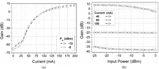
between the output power and the input power (Pout - Pin), in dB scale. Fig. 2(a) shows the gain vs.
current and Fig. 2(b) the gain vs. optical input power for the commercial SOA.
Fig. 1. Block diagram for the experimental setup.
(a) (b)
Fig. 2. SOA experimental results: (a) gain vs. bias current for input powers (Pin) equal to -5 and -12 dBm; (b) gain vs. Pin for
bias currents equal to 40, 60, and 150 mA.
The SOA active cavity’s length was obtained from the distance between residual Fabry-Perot modes [17], which can be seen in the ASE spectrum for high bias current (~200 mA). The finite facet
reflectivity produces spurious longitudinal modes, and from their spacing the longitudinal length can
Brazilian Microwave and Optoelectronics Society-SBMO received 10 Jan 2018; for review 23 Jan 2018; accepted 06 Jun 2018 m n L g
2 2 (1)where λ = 1550 nmis the central wavelength, ng = 3.86 is the effective refractive index for the active
cavity, and Δλ = 0.48 nm is the ripples’ wavelength spacing. B. Simulations
The TLM approach is widely used to model the light amplification inside the SOA [19]-[21]. In
such approach the behavior of each TLM section must be considered as an interplay between the
optical and the electronic populations [16]. Such modelling can be useful for numerical prediction on
optical networks, but it requires proper calibration – otherwise non-realistic predictions appear easily. So, the device characterization must be properly designed and performed, and be equally validated for
different models of commercial, black-box SOAs.
Before starting the model calibration, the SOA length must be determined, as shown above (Eq.1).
After, the parameters listed in Table I are changed individually to observe and analyze their impact
over the aforementioned optical gain curves. In order to do this, parameter sweep is performed for a
range of values below and above a default start, preconfigured in the numerical model. These
parameters are used in the rate equations and applied to the wave equations which are used to model
the propagation of the optical signal within the SOA active region. The solutions of these equations
are obtained numerically using the TLM method [16].
TABLE I. PARAMETERS FOR SOA MODEL – DEFAULT AND CALIBRATED
Parameter Default Calibrated
Active Region Type MQW MQW
Width of Active Region 2.5 µm 2.5 µm
Cavity Length 650 µm 650 µm
Thickness of Active Region 40 nm 100 nm
Thickness of the SCH Region 210 nm 210 nm
Injection Efficiency Coefficient (Icoeff) 1 0.85
Internal Losses Cefficient (ILC) 3000 m-1 4000 m-1
Internal Loss Carrier Dependence (ILCD) 1∙10-23 m2 1.1∙10-21 m2
MQW Confinement Factor 0.07 0.165
SCH Confinement Factor 0.56 0.56
Optical Coupling Efficiency (OCE) 1 0.4
Linear Gain Coefficient (Gcoeff) 3∙10
-20
m2 8.7∙10-20 m2
Carrier Density Reference Gain Shape (Nref) 2∙10
24
m-3 2∙1024 m-3
Carrier Density in the Transparency (CDT) 1.5∙1024 m-3 1.7∙1024 m-3
Initial Carrier Density (ICD) 1∙1024 m-3 0.3∙1023 m-3
Nonlinear Gain Coefficient (ε) 1∙10-23 m3 1∙10-23 m3
Linear Recombination (Arecomb) 1∙10
7
s-1 5∙108 s-1
Bimolecular Recombination (Brecomb) 1∙10
-16
m3∙s-1 1∙10-17 m3∙s-1
Auger recombination (Crecomb) 1.3∙10
-41
m6∙s-1 10∙10-41 m6∙s-1
Carrier Capture Time Constant (Capture Time) 7∙10-11 s 1∙10-11 s
Carrier Escape Time Constant (Escape Time) 14∙10-11 s 14∙10-11 s
First, the optical confinement factor and the cavity’s transversal sizes are parameters of greatest interest. Therefore, those parameters should are the first to be tested. The confinement factor is related
Brazilian Microwave and Optoelectronics Society-SBMO received 10 Jan 2018; for review 23 Jan 2018; accepted 06 Jun 2018 relationship of the three size dimensions, ie. total volume, to the confinement also determines the
SOA output saturation power [22].
To analyze the mutual relationship between those, a parallel sweep was performed combining the
confinement factor and the width and thickness of the active cavity and, thus, find the best match to
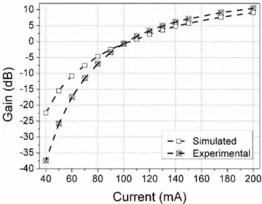
the experimental data for the profiles of gain vs current and of gain vs Pin. Figure 3 shows a case
where good approximation is reached – optimized at 2.5 µm, 100 nm, and 0.17, respectively. But a better adjust is still needed for the 40-80 mA range, where simulated and experimental curves differs
substantially. Some preconfigured parameters may have their default value out of the actual value,
and this may depend on factors such as the SOA dimensions (length, width, and thickness), the
semiconductor material (InGaAsP, InGaAs, etc.), SOA structure (bulk, MQW, QD, guided index, and
guided gain), etc. For that, the other parameters of Table I must be considered, such as CDT, ICD,
Nref, Gcoeff, ε, Arecomb, Brecomb, Crecomb, Icoeff, OCE, ILC, ILCD, capture time and escape time, that can be
varied to achieve better matchings.
Fig. 3. Gain vs. bias current for the SOA model - length = 0.65 mm, width = 2.5 μm, thickness = 100 nm, confinement factor = 0.17, input power = -5 dBm.
The CDT refers to the density of carriers to reach transparency, i.e. when the optical gain surpasses
all losses (gain = 0 dB). The ICD refers to the device’s intrinsic carrier’s density. The amplifier optical gain is linearly dependent on the electronic carrier’s density, with parabolic shaped spectra, and with effective bandwidth as function of the electronic density; the parameter Nref models the
reference carrier density for that. The amplifier gain is also afunction of the differential gain (dg/dN)
[23], adjusted by Gcoeff. The parameter ε contributes to the amplifier gain compression since the gain
saturation occurs at very high photon density. The physical origin of this nonlinear gain coefficient is
mainly the spectral hole burning [16].
The parameter Arecomb represents the nonradiative recombination process of carriers by crystal
defects (traps), that may occur in the active region during SOA fabrication and also when the device
Brazilian Microwave and Optoelectronics Society-SBMO received 10 Jan 2018; for review 23 Jan 2018; accepted 06 Jun 2018 linear effect is known as linear recombination coefficient, being significant for low current injection
[23].
The parameter Brecomb models the interaction of two carriers, an electron in the conduction band and
a hole in the valence band, meeting and recombining to produce light by spontaneous emission, whose
small portion is coupled to the active waveguide [23]. The Crecomb models the most important
non-radiative recombination, the so called Auger, involving three particles that exchange energy without
irradiation.
The parameter Icoeff designates the portion of the SOA injected current reaching the active region.
This current may partially deviates around the SOA electric contact, reducing so its contribution to the excited carriers’ population in the conduction band. The parameter OCE, by its very name, represents the portion of optical power that is coupled to the amplifier coming from an optical fiber.
The parameter ILC also plays an important role in the effective optical gain, so that internal losses
are due to Rayleigh scattering of light, absorption of photons by material resonances, and non-uniform distribution of the optical field in the waveguide [24]. The parameter ILCD changes by carriers lateral
spreading and non-radiative electron-hole recombination (phonons) [19].
The capture time refers to the capture of carriers by the quantum well, after these carriers cross the
SCH region. The escape time of carriers on the active region occurs through the thermionic emission
of these carriers.
III. RESULTS AND DISCUSSIONS
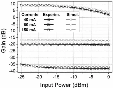
The adjustments for the gain vs. current and gain vs. Pin profiles were done based on the model
behavior, as presented in the previous section. The Fig. 4 and Fig. 5 show the experimental and
numerical results after our calibration procedure.
The calibrated parameters (Table I) differ from default ones as explained: the active region was
found thicker (100 nm) than the standard value (40 nm), correction based on the transparency current
(see Fig. 2(a)), greater than the default set. The confinement factor differs from the standard value
(0.07 to 0.165) because it is proportional to the cross-sectional area of the active region. Thus, for an
increase in thickness, an increase in the confinement factor is expected. The injection efficiency coefficients (Icoeff) models the fact that only part of the injected carriers reaches the active region,
while some diffuse around the metal contact and the semiconductor, and so the calibrated value is
lower than the ideal. The internal loss coefficient (ILC) of the calibrated model (4000 m-1) is also
bigger than default (3000 m-1), since the internal loss is higher in thicker active regions. The
fiber-to-waveguide coupling is not perfect, and so the optical coupling efficiency (OCE) is lower than 100%,
ranging from 20% to 70% [16].
The linear gain coefficient (Gcoeff) varied from 3x10
-20
m2 to 8.7x10⁻²⁰ m2 due to the strong
dependence on the number of quantum wells, generally equal to or greater than 12 [25]. As mentioned
Brazilian Microwave and Optoelectronics Society-SBMO received 10 Jan 2018; for review 23 Jan 2018; accepted 06 Jun 2018 of carriers in the transparency (CDT) increased from 1.5x1024 m-3 to 1.7x1024 m-3. The initial carrier
density (ICD) can be used to converge the gain/current curve. Thus, the ICD value for the calibrated
SOA was lower than default for convergence at low currents.
The Linear Recombination (Arecomb) is proportional to defects during fabrication or to the SOA
operation time (aging), and is significant at low currents. Thus, it was set at 5x10⁸ s-1 to reduce the
calibrated gain for low currents. Parameters such as capture time, Brecomb and Crecomb were used to
adjust the saturation curves and the convergence of the gain/current curve. Several authors have found
different values for the Crecomb as 7.5x10 -41
m6s-1 (1.55 µm - GaInAsP) [26], 9.8x10-41 m6s-1 (1.65 µm -
GaInAsP) [26], and 2.6x10-41 m6s-1 (1.3 µm - InGaAsP) [27].
The difference between the
experimental and simulated results seen in Fig. 4 (from 40 up to 80 mA) and Fig. 5 (from -25
up to 8 dBm and 60 mA current) shows the difficulties to adjust multi values for all model
parameters.
(a) (b)
Fig. 4. Gain curve vs. bias current for the calibrated model and the experimental results: Pin (a) -5 dBm (b) -12 dBm.
Brazilian Microwave and Optoelectronics Society-SBMO received 10 Jan 2018; for review 23 Jan 2018; accepted 06 Jun 2018
IV. CONCLUSION
A simple technique for calibration of numerical parameters for modelling of black-box, commercial
SOAs was presented. The adjustment of the gain/current and gain/Pin curves is based on experimental
data and parameters’ optimization. Through this technique, it was possible to calibrate three main parameters such as thickness, width and confinement factor of the active region of a commercial
SOA, among other important parameters. Thus, the calibrated model can be used in simulations to
predict several types of optical sub-systems, mainly with respect to amplification and distortions
caused by such devices.
ACKNOWLEDGMENT
The authors thank to the Brazilian agencies CAPES (scholarship), CNPq (contracts: 159388/2017-1, 400129/2017-5, 402923/2016-2, 301409/2017-0), and FAPESP (contracts: 2017/20121-8, 2014/18791-7, 2015/50063-4, 2007/56024-4).
REFERENCES
[1] T. Durhuus, B. Mikkelsen, C. Joergensen, S.L. Danielsen, K.E. Stubkjaer, All optical wavelength conversion by semiconductor optical amplifiers, J Lightwave Technol 14 (1992), 942–945.
[2] C. M. Gallep, A. L. R. Cavalcanti, N. S. Ribeiro, and E. Conforti, Nonhomogeneous current injection for the enhancement of semiconductor optical amplifier-based wavelength converters, Microwave Opt Technol Lett 48 (2006), 1141-1144.
[3] D. Brunina, D. Liu, and K. Bergman, An energy-efficient optically connected memory module for hybrid packet- and circuit-switched optical networks, IEEE J Sel Topics Quantum Electron 19 (2013).
[4] T. Tanemura, I. M. Soganci, T. Oyama, T. Ohyama, S. Mino, K. V. Williams, N. Calabretta, H. J. S. Dorren, and Y. Nakano, Large-Capacity Compact Optical Buffer Based on InP Integrated Phased-Array Switch and Coiled Fiber Delay Lines, J Lightwave Technol 29 (2011), 396–402.
[5] A. Ehrhardt, M. Eiselt, G. Grossopf, L. Kuller, R. Ludwig, W. Pieper, R. Schnabel, and H. G. Weber, Semiconductor laser amplifier as optical switching gate, J Lightwave Technol 11 (1993), 1287–1295.
[6] M. Renaud, M. Bachmann, and M. Erman, Semiconductor Optical Space Switches, IEEE J Sel Topics Quantum Electron, vol. 2, no. 2, Jun 1996.
[7] R. C. Figueiredo, T. Sutili, N. S. Ribeiro, C. M. Gallep, and E. Conforti, Semiconductor Optical Amplifier Space Switch With Symmetrical Thin-Film Resistive Current Injection, J Lightwave Technol 35 (2017), 280-287.
[8] R. C. Figueiredo, N. S. Ribeiro, A. M. Oliveira, C. M.Gallep, and E. Conforti, Hundred-Picoseconds Electro-Optical Switching With Semiconductor Optical Amplifiers Using Multi-Impulse Step Injection Current, J Lightwave Technol 33 (2015), 69-77.
[9] A. Chiuchiarelli, C. M. Gallep, and E. Conforti, Fabry-Perot laser-based optical switch for multicast transmission in bidirectional optical access networks, Microwave and Opt Technol Lett 58 (2016), 1466-1469.
[10]N. S. Ribeiro, C. M. Gallep, and E. Conforti, Semiconductor optical amplifier cavity length impact over data erasing/rewriting, Microwave Opt Technol Lett 55 (2013), 998-1001.
[11]L. Xi, Y. Ma, and L. Sun, Regeneration of DQPSK signals using semiconductor optical amplifier-based phase regenerator, in Int. Conf. on Advanced Infocom Technology, 2011: pp. 1.
[12]G. Gavioli and P. Bayvel, Novel 3R regenerator based on polarization switching in a semiconductor optical amplifier-assisted fiber Sagnac interferometer, IEEE Photonics Technol Lett 15 (2003), 1261.
[13]P. Vorreu, A. Marculescu, J. Wang, G. Bottger, B. Sartorius, C. Bornholdt, J. Slovak, M. Schlak, C. Schmidt, S. Tsadka, W. Freude, and J. Leuthold, Cascadability and regeneration properties of SOA all-optical DPSK wavelength
converters”, IEEE Photonics Technol Lett 18 (2006), pp.1970-1972.
[14]Y. Zhan, Min Zhang, Mintao Liu, Lei Liu, and Xue Chen, All-Optical Signal Regeneration Based on XPM in Semiconductor Optical Amplifiers, Asia Communications and Photonics Conference, 2012.
[15]P. Rocha, C. M. Gallep, and E. Conforti, All-optical mitigation of amplitude and phase-shift drift noise in semiconductor optical amplifiers, Optical Engineering 54(10), 2015.
[16]VPItransmissionMaker, “Photonics circuits user’s manual”.
[17]C. M. Gallep, Redução do tempo de chaveamento eletro-óptico em amplificadores ópticos a semicondutor, PhD thesis in Portugueese, FEEC-UNICAMP, 2003.
[18]S. M. Sze, and K. K. Ng, Physics of Semiconductor Devices, 3a ed., John Wiley & Sons, New Jersey, EUA, 2007. [19]A.J. Lowery, A new dynamic semiconductor laser model based on the transmission line modelling method, IEEE Proc J
Brazilian Microwave and Optoelectronics Society-SBMO received 10 Jan 2018; for review 23 Jan 2018; accepted 06 Jun 2018 [20]A.J. Lowery, Transmission-line modelling of semiconductor lasers: the transmission-line laser model, Int. J. Numerical
Modelling 2 (1989), 249–265.
[21]A. J. Lowery, Transmission-line laser modelling of semiconductor laser amplified communications systems, IEEE Proc J Optoelectron 139 (1992), 180–188.
[22]A. Das Barman, M. Scaffardi, S. Debnath, L Potì, and A. Bogoni, “Design tool and its experimental validation for SOA-based photonic signal processing”, Optical Fiber Techonol 15 (2009), 39-49.
[23]M. Conelly, Semiconductor Optical Amplifiers, Springer, New York, EUA, 2004.
[24]L. Gua-Dong, W. Chong-Qing, W. Fu, and M. Ya-Ya, Measurement of the internal loss coefficient of semiconductor optical amplificers, Chinese Phys Lett 30 (2013), 058501.
[25]M. C. Tatham, I. F. Lealman, C. P. Seltzer, L. D. Westbrook, and D. M. Cooper, Resonance frequency, damping, and differential gain in 1.5 µm multiple quantum-well lasers, IEEE J Quantum Electron 28 (1992), 408-414.
[26]E. Wintner, and E. P. Ippen, Nonlinear carrier dynamics in GaxIn1-xAsyP1-y compounds, Appl Phys Lett 44 n° 2, 1984.