Departamento de Engenharia Electrotécnica e de Computadores
Projecto de um circuito conversor DC-DC para aplicações de
“energy harvest”
José David Lopes Lameiro
Dissertação apresentada na
Faculdade de Ciências e Tecnologia da Universidade Nova de Lisboa para a obtenção do grau de Mestre em Engenharia Electrotécnica e de Computadores
Orientador: Doutor Nuno Filipe Silva Veríssimo Paulino
Composição do Júri:
Presidente: Doutor Adolfo Sanchez Steiger Garção – FCT/UNL
Vogais: Doutor Jorge Manuel dos Santos Ribeiro Fernandes – IST/UTL Doutor Luís Augusto Bica Gomes de Oliveira – FCT/UNL Doutor Nuno Filipe Silva Veríssimo Paulino
I
Copyright
Projecto de um circuito conversor DC-DC para aplicações de “energy harvest”© José David Lopes Lameiro
A Faculdade de Ciências e Tecnologia e a Universidade Nova de Lisboa têm o direito, perpétuo e sem limites geográficos, de arquivar e publicar esta dissertação através de exemplares impressos reproduzidos em papel ou de forma digital, ou por qualquer outro meio conhecido ou que venha a ser inventado, e de a divulgar através de repositórios científicos e de admitir a sua cópia e distribuição com objectivos educacionais ou de investigação, não comerciais, desde que seja dado crédito ao autor e editor.
III
Acknowledgments
Firstly, I would like to thank my girlfriend (Catarina), parents and sister for all the love and support they have given me over the course of my life.
I’m extremely grateful to my advisor, Prof. Nuno Paulino, for being more than a mentor, giving all the support and encouraging me when I needed.
Special thanks to Carlos Carvalho, for have given a marvellous start up work and for having spent a lot of time helping me.
V
UNIVERSIDADE NOVA DE LISBOA
Resumo
Faculdade de Ciências e Tecnologia
Departamento de Engenharia Electrotécnica e de Computadores
Mestre em Engenharia Electrotécnica e de Computadores
por José David Lopes Lameiro
Esta tese apresenta um circuito conversor DC-DC (“step-up”) para aplicações de “energy harvest”. Este circuito utiliza uma arquitectura “Switched capacitor voltage tripler”, controlada por um circuito MPPT baseado nos métodos “Load Voltage Maximization” e “Hill Climbing”. Este circuito foi desenhado usando a tecnologia “0.13 μm CMOS” de forma a funcionar com uma célula fotoeléctrica de “a-silicon”. Este circuito tem uma fonte de alimentação local também controlada pelo mesmo circuito MPPT, que é uma réplica do conversor “SC voltage tripler”, redimensionado a 3% da área deste último. Este circuito utiliza a combinação de transístores PMOS e NMOS de forma a reduzir a área ocupada. Um esquema de reutilização de cargas é utilizado para compensar as grandes resistências parasitas associadas aos transístores MOS. Os resultados das simulações mostram que o circuito pode fornecer uma potência de 9636 μW à carga, utilizando uma potência de 1274 μW na célula fotoeléctrica, correspondendo a uma eficiência na ordem dos 75,66%. As simulações mostram também que o circuito é capaz de se iniciar com apenas 19% do nível de iluminação máximo da célula fotoeléctrica.
Palavras-Chave: Energy harvesting, conversor DC/DC, baixa potência, CMOS, Load Voltage Maximization, Hill Climbing.
VII
UNIVERSIDADE NOVA DE LISBOA
Abstract
Faculdade de Ciências e Tecnologia
Departamento de Engenharia Electrotécnica e de Computadores
Mestre em Engenharia Electrotécnica e de Computadores
by José David Lopes Lameiro
This thesis presents a step-up micro-power converter for solar energy harvesting applications. The circuit uses a SC voltage tripler architecture, controlled by a MPPT circuit based on the Load Voltage Maximization and the Hill Climbing methods. This circuit was designed in a 0.13 μm CMOS technology in order to work with an a-silicon PV cell. The circuit has a local power supply voltage, created using a scaled down SC voltage tripler, controlled by the same MPPT circuit, to make the circuit robust to load and illumination variations. The SC circuits use a combination of PMOS and NMOS transistors to reduce the occupied area. A charge re-use scheme is used to compensate the large parasitic resistors associated to the MOS transistors. The simulation results show that the circuit can deliver a power of 9636 μW to the load using 1274 μW of power from the PV cell, corresponding to an efficiency as high as 75.66%. The simulations also show that the circuit is capable of starting up with only 19% of the maximum illumination level.
Keywords: Energy harvesting, DC/DC converter, low power, CMOS, Load Voltage Maximization, Hill Climbing.
IX
Contents
ACKNOWLEDGMENTS ... III RESUMO ... V ABSTRACT ... VII LIST OF FIGURES ... XI LIST OF TABLES ... XIIIABBREVIATIONS ... XV
CHAPTER 1 ... 1
INTRODUCTION ... 1
1.1 Background and Motivation ... 1
1.2 Thesis Organization ... 2
1.3 Contributions ... 3
CHAPTER 2 ... 5
STATE OF THE ART ... 5
2.1 Amorphous Silicon Solar Cell ... 5
2.1.1 Introduction ... 5
2.1.2 Results and discussion ... 6
2.2 Switched capacitor step-up voltage tripler circuit with charge reusing ... 7
2.2.1 Introduction ... 7
2.2.2 Overview of the circuit ... 10
2.2.3 The principle of operation of the step-up converter ... 11
2.2.4 Local power supply ... 11
CHAPTER 3 ... 13
MAXIMUM POWER POINT TRACKING ... 13
3.4 Photovoltaic Cell Maximum Power Point Tracking Techniques ... 14
3.1.1 Hill-climbing/Perturb and Observe (P&O) ... 15
3.1.2 Fractional VOC ... 17
3.1.3 RCC ... 17
3.1.4 Load I or V Maximization ... 19
3.1.5 Analysis and discussion of the different MPPT techniques ... 20
CHAPTER 4 ... 23
PHASE GENERATION AND CONTROL ... 23
4.4 Overview ... 23
4.4 Delay circuit ... 25
4.2.1 Introduction ... 25
4.2.2 Fixed Delay circuit ... 27
4.2.3 Variable Delay circuit ... 29
4.4 Maximum Power Point Control Module ... 31
4.3.1 Comparator ... 32
The value of Vbiasn is 0.178V and Ibiasn is 182.8nA. ... 33
X
4.4 Start-up circuit ... 35
CHAPTER 5 ... 37
SIMULATION RESULTS ... 37
CHAPTER 6 ... 47
CONCLUSIONS AND FUTURE WORK ... 47
6.1 Conclusions ... 47
6.2 Future Work ... 48
BIBLIOGRAPHY ... 49
APPENDIX A ... 51
LOGICAL GATES – ADDITIONAL SCHEMATICS ... 51
A.1 NAND ... 51
A.2 NOR ... 52
A.3 NOT ... 52
A.5 Flip-Flop Type RS ... 53
A.6 Flip-Flop Type D ... 54
A.7 Switch ... 54
APPENDIX B ... 55
PUBLICATION SUBMITTED IN THE IEEE INTERNATIONAL SYMPOSIUM ON CIRCUITS AND SYSTEMS 2011 ... 55
I. INTRODUCTION ... 57
II. AMORPHOUS SILICON SOLAR CELL ... 57
III. SWITCHED CAPACITOR STEP-UP VOLTAGE TRIPLER CIRCUIT WITH CHARGE RE-USE ... 58
IV. HILL CLIMBING MAXIMUM POWER POINT TRACKING ... 58
V. PHASE GENERATION AND CONTROL ... 59
VI. SIMULATION RESULTS ... 59
XI
List of Figures
1-1: Block Diagram of Pv Cell Power Management System ... 2
2-1: Equivalent Electrical Circuit of the Amorphous Silicon Pv Cell ... 6
2-2: Power And Current Curves of the Solar Cell Equivalent Circuit Model ... 6
2-3: Simplified Schematic of the Step-Up Voltage Converter ... 7
2-4: Equivalent Model of Integrated Capacitor with its Parasitic Elements. ... 9
2-5: Step-Up Sc Voltage Tripler Circuit ... 10
3-1: Current Vs. Voltage For A Pv Cell ... 14
3-2: Characteristic Pv Cell Power Curve ... 15
3-3: Divergence Of Hill Climbing/P&O From Mpp ... 16
3-4: Schematic Diagram of Proposed Mppt using the Rcc Method [16] ... 18
3-5: Different Load Types ... 19
3-6: Step-Up Sc Voltage Tripler Circuit ... 21
5-2: Phases generated by the Synchronous State Machine (ASM) ... 24
4-1: Schematic of the Phase Controller ... 24
4-3: Shunt Capacitor Delay Element ... 26
4-4: Current Starved Delay Element ... 27
4-5: Fixed Delay Circuit ... 28
4-6: Variable Delay Circuit ... 29
4-7: Maximum Power Point Control Module Circuit ... 31
4-8: Signals of the Maximum Power Point Control Module Unit ... 32
4-9: Three-Stage Comparator (Bias Circuit not shown) ... 34
4-10: Switch In Drain Single-Ended Charge Pumps ... 35
4-11: Start-Up Circuit Schematic ... 35
5-1: Evolution of Vin, Vdd, Vout and Vvco, During Start-Up and Transient Operation (Illumination of 100% And 17.5%, Changing At 150μs) ... 38
5-2: Evolution of Vin, Vdd, Vout and Vvco, During Start-Up and Transient Operation (Illumination of 19% And 100%, Changing at 600μs) ... 39
5-3: Evolution of Vin, Vdd, Vout and Vvco, during Start-Up and Transient Operation (Illumination Of 100% And Load Resistance Changing At 250μs From 1 kΩ To 100Ω) ... ... 40
5-4: Evolution of the Efficiency of PV Power at 100% Light Intensity Under Different Output Resistor Values ... 41
XII
5-5: Evolution of the Efficiency of PV Power Under four Different Light Intensities and
Different Output Resistor Values ... 44
5-6: Evolution of The Efficiency of PV Power under four Different Light Intensities and Different Operating Frequencies ... 45
5-7: Evolution of the Efficiency of PV Power under four Different Light Intensities and Different Input Power (Pin) ... 46
A.1: A) Schematic of NAND ... 51
A.2: A) Schematic of NOR. ... 52
A.3: A) Schematic of NOT. ... 52
A.4: A) Schematic of XNOR. ... 53
A.5: A) Schematic of Flip-Flop Type RS. ... 53
A.6: A) Schematic of Flip-Flop Type D. ... 54
XIII
List of Tables
3-I Summary of Hill Climbing algorithm ... 16 4-I Summary of Hill Climbing algorithm ... 32 4-II Comparator mosfet sizes ... 33 5-I Relevant Parameters of the Circuitfor the Different Output Resistor Values
... 41 5-II Relevant Parameters of the Circuitfor the Different Output Resistor Values And 19% Light Intensity ... 42 5-III Relevant Parameters of the Circuitfor the Different Output Resistor Values And 50% Light Intensity ... 43 5-IV Relevant Parameters of the Circuitfor the Different Output Resistor Values And 75% Light Intensity ... 43 A.1 Truth table of Flip-Flop type RS. ... 54
XV
Abbreviations
AM1 Air Mass 1
ASM Asynchronous State Machine
CMOS Complementary Metal-Oxide Semiconductor
COX Gate-oxide capacitance per unit area
DC Direct Current
DSP Digital Signal Processor
ITO Indium Tin Oxide
MOSFET Metal Oxide Semiconductor Field Effect Transistor
MPP Maximum Power Point
MPPT Maximum Power Point Tracking
NMOS N-Channel Metal Oxide Semiconductor Field Effect Transistor PMOS P-Channel Metal Oxide Semiconductor Field Effect Transistor
PECVD Plasma Enhanced Chemical Vapor Deposition
P&O Perturb and Observe
PV Photovoltaic
Rf-PERTE radio-frequency Plasma Enhanced Reactive Thermal Evaporation
SC Switched capacitor
VMPPT Voltage-based Maximum Power Point Tracking
Chapter 1 - Introduction
1
Chapter 1
Introduction
1.1 Background and Motivation
Energy harvesting or energy scavenging is the process by which energy is derived from external sources (e.g. solar power, thermal energy, wind energy, salinity gradients, and kinetic energy), captured and stored. Energy harvesting has an advantage over energy derived from fossil fuels or provided by batteries because it is a renewable type of energy, and more environmentally friendly. So, Energy harvesting devices convert ambient energy into electrical energy.
Looking around, there are plenty devices that could be more autonomous, i.e. it may not be practical to plug a device to a power grid, nor to use batteries, as they need to be replaced when their charge is depleted. And all of these devices have the same problem, so the question is how can they be powered without these restraints? The answer is: these applications can be powered by collecting the energy that exists in the surrounding environment (energy harvesting). By employing energy harvesting, circuits can virtually operate permanently. Although there are different ambient energy sources available, ambient light has the highest energy density when compared to other possible ambient energy sources [1] and it can easily be harvested by using photovoltaic (PV) cells.
A photovoltaic cell (which is essentially a diode) converts light energy directly into electrical energy. The output voltage of a single photovoltaic cell (PV) is at the most 0.7 V (under open circuit conditions) and can be as low as 0.4 V under maximum power condition. This means that it is necessary to have a voltage step-up (Figure 1-1) circuit that can increase
Chapter 1 - Introduction
2
the PV voltage to acceptable values, in order to power a Complementary Metal-Oxide Semiconductor (CMOS) circuit (typically larger than 1.0 V).
A small size system will necessarily have a small PV cell which will limit the power available to the step-up converter.
Under low power conditions, it is feasible to use a capacitor based instead of an inductor based voltage step-up converter, allowing the reduction of the system size. Since the power and the voltage produced by a PV cell varies with the connected load and with the amount of incident light, it is necessary for the step-up to compensate for this variation in order to supply the maximum power available to the load. This means that the step-up converter should adjust its behaviour in order to track the maximum power point (MPP) of the PV cell. There are several methods available for determining the MPP of a PV cell (Figure 1-1). Most of these methods are not suitable for low power applications because they require complex implementations that dissipate a lot of power [2].
Figure 1-1: Block diagram of PV cell power management system
1.2 Thesis Organization
This thesis has been organized in seven chapters including this introductory one.
A section with the introduction, results and discussion of the Amorphous Silicon Solar Cell will be explained in Chapter 2. Also in Chapter 2, the Switched Capacitor DC-DC Converter will be introduced. A section with the circuit’s overview of this study is also included. Chapter 3 gives an in depth analysis about the Maximum Power Point Tracking used in this study. Starting with a theoretical analysis, where some different MPPT techniques will be explained and discussed. Finally, the techniques chosen for this work and the reasons behind it will be explained.
Chapter 1 - Introduction
3
Chapter 4 will focus on the Phase generation and control, where all the relevant sub-modules of Phase Control circuit will be explained. A section with the explanation of Start-Up module is also included.
In Chapter 5, the results of some simulations in 130 nm CMOS technology will be presented.
Chapter 6 is reserved for overall conclusions and further research suggestions.
1.3 Contributions
Most of the existent Solar Harvest Systems are made to deliver medium or large amounts of Power (more than 1W). There is a lack of circuits that are able to work with Power levels smaller than around 1mW. The main contribution of this thesis is that it gives a solution for Solar Harvest Systems with an operating power below 1mW.
The present work has originated a paper (Appendix B) that was accepted for publication at the International Symposium on Circuits and Systems 2011 (ISCAS 2011).
Chapter 1 - Introduction
Chapter 2 – State of the art
5
Chapter 2
State of the art
This chapter will introduce an explanation of how the system globally works. The behavior of the amorphous Silicon solar cell will be described. A section with the results and discussion of this study is also included below. Some theory about Switched Capacitor DC-DC Converter will be also introduced.
2.1 Amorphous Silicon Solar Cell
2.1.1 Introduction
In order to reduce the size of the energy harvesting system, an a-Silicon PV cell was chosen, this cell was built by depositing amorphous silicon with a structure p/i/n on a glass previously covered with ITO (Indium Tin Oxide). The ITO was deposited using rf-PERTE (radio-frequency Plasma Enhanced Reactive Thermal Evaporation) and had a sheet resistance of 35 Ω/ . The active p-type, intrinsic and n-type layers were deposited using PECVD (Plasma Enhanced Chemical Vapor Deposition) and had a thickness of 150Å, 4500Å and 500Å respectively. The frontal aluminum electrode was deposited using thermal evaporation [3]. The die containing the step-up converter (and other circuitry) can be glued to the cell and connected to the PV cell terminals. The PV cell was experimentally characterized and an equivalent electrical model, shown in Figure 2-1 , was obtained.
Chapter 2 – State of the art
6
Figure 2-1: Equivalent electrical circuit of the amorphous silicon PV cell
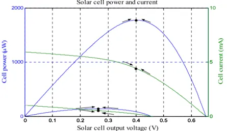
2.1.2 Results and discussion
By simulation on Cadence, the cell has a short circuit current of about 5.9 mA, a maximum power of 1775 μW that occurs for a voltage of 403 mV (maximum power point) and an open circuit voltage of 652 mV. These data refer to a cell having an active area of about 1 cm2, when irradiated according to AM1 (Air Mass 1) conditions (irradiance by the solar
spectrum at the earth surface, having the Sun vertically located). The resulting power and current curves of the cell for AM1 and 20% of AM1 conditions are depicted in Figure 2-2.
0 0.1 0.2 0.3 0.4 0.5 0.6 0 1000 2000 C ell p ow er ( μ W)
Solar cell output voltage (V) Solar cell power and current
0 0.1 0.2 0.3 0.4 0.5 0.6 0 5 10 C ell c urre nt (m A ) 0 0.1 0.2 0.3 0.4 0.5 0.6 0 5
Chapter 2 – State of the art
7
2.2 Switched capacitor step-up voltage tripler circuit with
charge reusing
2.2.1 Introduction
2.2.1.1 Switched Capacitor DC-DC Converter s
Switched capacitor (SC) DC-DC converters (charge pumps) [4] are widely used in applications where a voltage higher than, or of the opposite polarity to, the input voltage is needed. A switched capacitor converter uses only capacitors and switches to perform the voltage conversion and hence does not need the magnetic storage elements used by inductor-based buck converters.
The Figure 2-3 shows a simplified schematic of the step-up (SC) voltage tripler [5].
Figure 2-3: Simplified schematic of the step-up voltage converter
During the phase φ1, the capacitors C1 and C2 are charged with the input voltage value
(vin). Then, during the phase φ2, the capacitors C1 and C2 are connect in series with the input
voltage source (vin), resulting in an output voltage (vdd) that is three times larger than the input
voltage value (that’s the reason of the name voltage tripler).
Assuming that the output of this circuit is connected to a load resistance (RL) in parallel
with a large external capacitance Co, the resulting equivalent circuit consists of a voltage source
(with a voltage value equal to 3vin) in series with two resistances. The first one is the equivalent
Chapter 2 – State of the art
8
output voltage of this circuit is the voltage division of 3vin by the resistive divider formed by
these two resistors. The output voltage will have a ripple that is inversely proportional to the value of Co. The value of this capacitance will regulate the upper limit of the output voltage,
being inversely proportional to it.
In this type of circuit, the frequency of the clock signal that controls the switches (phases φ1 andφ2) changes dynamically the equivalent resistance of the switched capacitors. So the
output voltage value (vdd) can be regulated by varying the frequency of the clock. For this reason,
the implementation of this type of circuit usually has a Phase Generator or controller module. Switched capacitor DC-DC converters are a viable option for such systems. One of the main drawbacks of traditional on-chip switched capacitor DC-DC converters is their low efficiency compared to regular switching converters.
2.2.1.2 Loss Mechanisms in a Switched Capacitor
DC-DC Converter Efficiency of a power converter is a key metric for battery operated electronics and energy starved systems. The main contributors to efficiency loss in a switched capacitor DC-DC converter are listed below.
2.2.1.2.1 Conduction loss in transferring charge from the PV cell to the load (battery)
This is the main loss mechanism which arises from charging a capacitor through a switch. When charge flows from the PV Cell to the load, some part of it is dissipated within the switches of the DC-DC converter.
2.2.1.2.2 Loss due to bottom-plate parasitic capacitors
The power lost due to the parasitic bottom-plate capacitors has a significant impact to the total power loss. The next figure illustrates an equivalent model of integrated capacitor with his parasitic elements, where Cpar1 and Cpar2 correspond to the bottom-plate and top-plate parasitic
Chapter 2 – State of the art
9
Figure 2-4: Equivalent model of integrated capacitor with its parasitic elements.
In this structure, the top-plate parasitic capacitances is clearly smaller than the bottom-plate parasitic capacitances, for this reason the power lost due to the parasitic elements is almost totally provided by the bottom-plate capacitors.
Therefore, each capacitor of the Figure 2-3 has bottom-plate parasitic capacitance, where CparB1 and CparB2 correspond to the bottom-plate parasitic capacitances of the capacitances C1
and C2. During the phase φ1, the capacitances C1 and C2 are connected in series and the
parasitic capacitances CparB1 and CparB2 are charged up with vin. During the phase φ2, the
capacitances C1 and C2 are charged up with vin, and the bottom-plate parasitic capacitances
CparB1, CparB2 are discharged. So in phase φ2, the system dissipates the power stored in the phase
φ1 by the parasitic bottom-plate capacitors.
2.2.1.2.3 Gate-drive loss
The power lost due to switching the gate capacitances of the charge-transfer switches is another significant contributor to the total power loss. The energy expended in switching the gate capacitances of the charge-transfer switches every cycle is directly related with Cox (the gate-oxide capacitance per unit area), WEFF (the cumulative width of switches that are turned
ON / OFF per cycle), Lmin (the minimum channel length of the technology node in which the
switched capacitor converter is implemented) and the output voltage value of the PV cell (vin).
2.2.1.2.4 Power loss in the control circuitry
The power lost in the control circuitry is given by the total power dissipated by all the control circuit of the system. This power is a function of the clock frequency and of the parasitic capacitances in the control circuit. Therefore it is necessary to use minimum size transistors wherever possible in order to reduce the power losses due to the control circuit.
Chapter 2 – State of the art
10
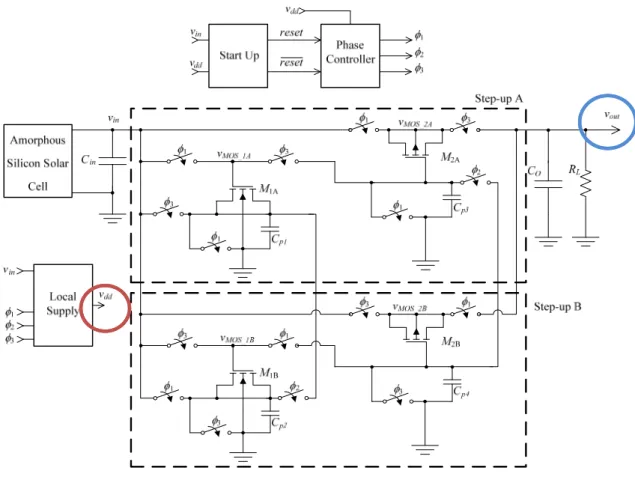
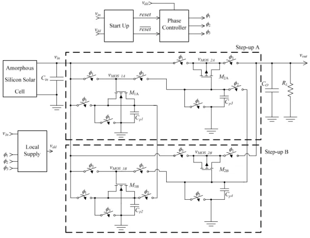
2.2.2 Overview of the circuit
The Figure 2-5 illustrates the schematic of Switched Capacitor Step-up voltage tripler circuit (circuit inside of the square). This circuit is connected in series with the input voltage source vin (provided by the Amorphous Silicon Solar Cell, already explained in chapter 2). If
there were no losses, the Step-up SC voltage circuit would provide an output voltage (vout), three
times larger than the input voltage value (vin). The output voltage (vout) is typically connected to
a large capacitor (CO), in order to reduce the output ripple and store energy.
The clock phases of the step up converter are generated by a phase controller circuit, and a Start Up circuit guarantees that, during start up, the phase generator is correctly initialized. These two circuits will be described in more detail in chapter 4.
There is a Local Power Supply used to guarantee the voltage supply for the Phase controller module (that will be explained in more detail further ahead in this chapter).
Chapter 2 – State of the art
11
2.2.3 The principle of operation of the step-up converter
The circuit of the SC step-up converter is shown in Figure 2-5. The principle of operation of this circuit is the same as the SC voltage tripler [5, 6]. In order to reduce the area of the circuit, MOS capacitors are used instead of MiM capacitors. During phase φ1, the MOS
capacitors of the upper half circuit (step-up A), M1A and M2A, are charged with the input voltage
value (vin) and then, during phase φ3, they are connect in series with the input voltage source. If
there were no losses, this would result in an output voltage (vout) three times larger than the input
voltage value.
The clock frequency and the capacitances values are dependent on the amount of power that must be transferred to the load. According to a theoretical analysis [6], the MOS capacitances that would yield the best efficiency were determined to be 4.2 nF. As such, the dimensions of the MOS transistors were set to achieve this capacitance value. For this value, the corresponding operating frequency of the system was determined to be about 1.5 MHz. The efficiency of this circuit (assuming that there are no parasitic losses) depends only on the values of the input and output voltages [5]. Since, during phase φ3, the drain/source voltage increases,
the threshold voltage of a NMOS transistor also increases (due to the body effect), resulting in a decrease of the capacitance of the transistor. This reduction can be significant for transistor M2A,
therefore this device is a PMOS instead of an NMOS transistor.
The other issue of using MOS capacitors is the large parasitic capacitance associated to the bottom plate nodes (drain/source nodes). In order to reduce the amount of charge lost in these parasitic capacitances, the circuit is split into two halves. The top half (A) is composed by M1A and M2A and the bottom half (B) is composed by M1B and M2B. The bottom half works in the
same way as the top half, with phase φ1 changed with phase φ3. During an intermediate phase
(φ2), the bottom nodes of both MOS capacitors of the upper and lower half-circuits are
connected together, thus transferring half of the charge in one parasitic capacitance to the other, before the bottom nodes are shorted to ground. This reduces by half the amount of charge that is lost in the parasitic capacitance nodes.
2.2.4 Local power supply
The output voltage of the circuit depends on the value of the load resistance RL (Figure
Chapter 2 – State of the art
12
circuit from working correctly. This means that the output voltage cannot be used to power the phase generator; therefore a smaller SC voltage step-up circuit, controlled by the same clock, is used to create a local power supply voltage (vdd). This circuit is a replica of the step-up circuits
(A + B), scaled to 3% of their area, as this ratio yielded the best results. This local power is decoupled internally with MOS capacitors.
Chapter 3 – Maximum power point tracking
13
Chapter 3
Maximum power point tracking
Tracking the maximum power point (MPP) of a photovoltaic (PV) cell is usually an essential part of a PV system, because as the name explains, that optimizes the amount of power transferred from the PV cell under a given temperature and irradiance.
PV systems have a single operating point where the values of the current (I) and Voltage (V) result in a maximum power output. These values correspond to a particular load resistance which is equal to:
Zin = (3.1)
A PV cell has an exponential relationship between current and voltage, and the MPP occurs at the knee of the curve (Fig 3.1), where the resistance is equal to the negative of the differential resistance:
Chapter 3 – Maximum power point tracking
14
Figure 3-1: Current vs. Voltage for a PV cell
Maximum power point trackers utilize some type of control circuit to search for this point and thus to allow the converter circuit to extract the maximum power available from a cell. This will be explained in more detail in next.
3.4 Photovoltaic Cell Maximum Power Point Tracking
Techniques
Many MPP tracking (MPPT) methods have been developed and implemented. The methods vary in complexity, sensors required, convergence speed, cost, range of effectiveness, implementation hardware, popularity, and in other respects. One of the main goals of this work is optimize the efficiency of the circuit composed by the PV cell and the step-up converter, so an implementation with a low consumption of power is an important factor in deciding witch MPPT technique to use. Therefore, an easy implementation, one that would not require the use of software and programming, would be a good option. Following the last criteria, some different MPPT techniques [7] were selected, that will be explained and discussed ahead. Finally, the techniques chosen for this work and the reasons behind it will be explained.
Chapter 3 – Maximum power point tracking
15
3.1.1 Hill-climbing/Perturb and Observe (P&O)
Hill climbing is a mathematical optimization technique which belongs to the family of local search. It is an iterative algorithm that starts with an arbitrary solution to a problem, then attempts to find a better solution by incrementally changing a single element of the solution.
Talking now about MPPT technique, the hill climbing method [8-15] involves a perturbation in the duty ratio of the step-up converter. The duty ratio of the step-up converter is the control variable of such kind of system. In the case of a PV cell connected to a step-up converter, perturbing the duty ratio of step-up converter perturbs the PV cell current and consequently perturbs the PV cell voltage. A variation of this method is to directly use the duty cycling of switching mode converter or inverter as a MPPT parameter and force dP/dD to zero, where P is the PV cell output power and D is the switching duty cycling of the step-up converter.
Figure 3-2: Characteristic PV cell power curve
In Fig. 3-2, it can be seen the characteristic of a PV cell power curve: an increase of voltage will lead to an increase of the power when operating on the left of the MPP, and when on the right of the MPP, an increase of the voltage will lead to a decrease of the power. This algorithm is summarized in Table 3-I.
Chapter 3 – Maximum power point tracking
16
Table 3-ISUMMARY OF HILL CLIMBING ALGORITHM [8]
Perturbation Change in Power
Next
Perturbation
Positive Positive Positive
Positive Negative Negative
Negative Positive Negative
Negative Negative Positive
The P&O method is a method of the Hill Climbing class. By definition, it involves a perturbation in the operating voltage of the PV cell. Therefore, Hill climbing and P&O methods are different ways to envision the same fundamental Method.
Figure 3-3: Divergence of hill climbing/P&O from MPP
Under rapidly changing atmospheric conditions, it is possible to have multiple local maxima with this method (as illustrated in Fig. 3-3). Starting from an operating point A, if atmospheric conditions stay approximately constant, a perturbation ΔV in the PV voltage V will bring the operating point to B and the perturbation will be reversed due to a decrease in power. On the other hand, if the irradiance increases and shifts the power curve from P1 to P2 within
one sampling period, the operating point will move from A to C. This represents an increase in power and the perturbation is kept the same. Consequently, the operating point diverges from the MPP and will keep diverging if the irradiance steadily increases. In the present case, this is not a problem because of the high sampling frequency (larger than 100kHz) which will make very unlikely for a significant illumination variation to occur within a sampling period.
Chapter 3 – Maximum power point tracking
17
3.1.2 Fractional V
OCThe fractional VOC method [15] or Voltage-based MPPT (VMPPT) algorithm is based on
the near linear relationship between VMPP (output voltage when it operates at MPP) and VOC
(open circuit voltage) of the PV cell, under varying irradiance and temperature levels. This relationship can be expressed by:
VMPP ≈ k1VOC (3.3)
where k1 is a constant of proportionality. Since k1 is dependent on the characteristics of the PV
cell being used, it usually has to be computed beforehand by empirically determining VMPP and
VOC for the specific PV cell at different irradiance and temperature levels. For the PV cell, K1 is
normally around 70% (between 0.71 and 0.78), depending on the materials, the surface condition of the cell and also the range of the incident light intensity.
For the circuit implementation of the fractional VOC method, the open circuit voltage (VOC)
of the PV cell is firstly measured. It can be done by momentarily shutting down the step-up converter. The MPP voltage can then be calculated according to the equation 4.3. The MPP voltage is used as a reference voltage to adjust the input impedance of the PV cell; consequently the voltage from the PV cell approaches the MPP voltage VMPP and the output power from the
PV cell is maximized accordingly.
This method is very easy and cheap to implement as it does not require a DSP or a microcontroller control. However, under changing atmospheric conditions, this method causes multiple local maxima (multiple erroneous maximum power points). In addition to this, the constantly shutting down of the step-up converter incurs some disadvantages, including temporary loss of power.
3.1.3 RCC
Ripple correlation control (RCC) makes use of converter ripple as an alternate source of perturbation. The MPP is usually located by correlating the derivative of the PV cell power (P) with the PV cell voltage (V) or current (I) ripple waveform (Equations 3.4 and 3.5).
Chapter 3 – Maximum power point tracking
18
(3.4)
or
(3.5)
Using the Fig. 3-2 to illustrate, if V or I is increasing (PV cell voltage or current derivative is positive) and P is increasing (PV cell power derivative is positive), then the operating point is below the MPP (V <VMPP or I < IMPP). However, if V or I is increasing (PV
cell voltage or current derivative is positive) and P is decreasing (PV cell power derivative is negative), then the operating point is above the MPP (V >VMPP or I > IMPP). Combining these
observations, the product of PV cell power and voltage derivatives with respect to time is zero at the MPP, but yields a positive and negative sign when the operating point is to the left or right (respectively) of the MPP.
Simple and inexpensive analog circuits can be used to implement RCC. An example is given in [16], with comparators, amp-ops, a multiplier, a D-type latch, a XOR gate and resistors (Fig 3-4).
In this schematic, the voltage and current are sensed for the PV cell to create two waveforms: the PV cell voltage and the PV cell power (by multiplication of the PV cell voltage and current). After that, the measured power and voltage waveforms are approximately differentiated using high pass filters and then compared with respect to a ground reference. Since each comparator has only binary states, there are four steady-state modes of operation. These modes are evaluated by an exclusive-OR gate and then sampled by a D-type flip-flop clocked at a constant frequency. The flip-flop output provides a suitable signal to drive a DC-DC converter switch.
Chapter 3 – Maximum power point tracking
19
As Midya et al. (1996:1710) note, a major benefit of RCC is that it ‘keeps [DC–DC] converter operation at the optimum point’ while avoiding the ‘inconvenient, slow, and fundamentally sub-optimal’ perturbation process described in previous sections. But this method can fail due to the phase shift brought about by the intrinsic capacitance of the PV cell at high switching frequencies.
The main disadvantage of this method is that it requires a multiplier block. An analog version of this block is difficult to implement and it can use more power than it is available for the installed application.
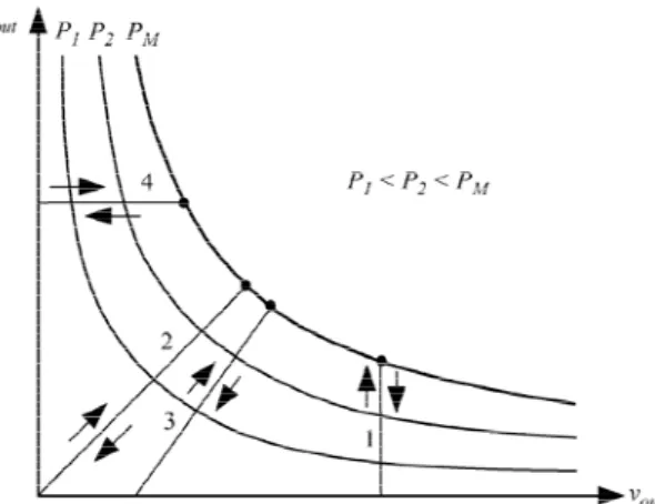
3.1.4 Load I or V Maximization
When the PV cell is connected to a step-up converter, maximizing the PV cell power also maximizes the output power at the load of the converter. Assuming a lossless converter, the inverse is also true, i.e., maximizing the output power of the converter should maximize the PV array power.
There are different load types: it can be of voltage-source type, current-source type, resistive type, or a combination of these [7]. As the Fig. 3-5 shows, if you have a voltage-source type load, to obtain the MPP, the load current iout should be maximized. For a current-source
type load, the load voltage vout should be maximized. For the other load types, either iout or vout
can be used. So, only one sensor is needed (iout or vout).
Figure 3-5: Different load types. 1: voltage source, 2: resistive, 3: resistive and voltage source, 4: current source.
Chapter 3 – Maximum power point tracking
20
In most PV systems, a large capacitor (battery) is used as the main load. In this case, it is very difficult to sense the variation of the load voltage and the load current can be used as the control variable (voltage-source type load) using a current sensor circuit [17].
3.1.5 Analysis and discussion of the different MPPT techniques
The amount of power transferred from the PV cell to the circuit depends on the impedance presented by the step-up converter to the PV cell (Zin). An increase in Zin leads to an
increase in the PV cell output voltage and a decrease in the output PV cell output current. The impedance should be adjusted in order to maximize the power of the PV cell. This means that if the PV voltage is lower than the MPP voltage the PV voltage should increase, if it is larger it should decrease (Figure 3-2). Since there is only a small amount of power available for the system, it is difficult to compute the power by performing a multiplication between the voltage and the current (RCC method); therefore a different approach should be followed. On the other hand, the fractional VOC method isn’t a good alternative, because: under changing atmospheric
conditions this method causes multiple local maxima (PV cell technically can operate at multiple MPP); it doesn’t control the impedance Zin; and the measurement of VOC includes
relevant loss of power. Now, only the Hill Climbing and Load I or V Maximization methods will be analysed and discussed.
In the circuit, the power delivered to the load depends on the output voltage and on the load resistance value. Assuming that the load resistance value is constant (or varies slowly), the variation of the power can be determined by measuring the variation of the output voltage. This means that the MPP can be found by maximizing the output voltage (Load voltage maximization method). In reality, this method maximizes the power delivered to the load and not the power from the PV cell [18]. This is preferable because the final objective should always be to maximize the efficiency of the system composed by the PV cell and the step-up converter and not simply to extract the maximum power from the cell at the expense of delivering less power to the load. However, since the output voltage is typically connected to a large capacitor, the amount of voltage variation would be extremely small and very difficult to detect. In order to solve this problem, the local power supply voltage (vdd) is monitored instead (Fig.3-6),
because it is a replica of the step-up converter (SC voltage tripler), but without a large capacitor connected on the output voltage (as explained in chapter 3 that power supply provides the vdd
voltage to all the local components). Note that if the load resistor decreases, this results in a decrease of the output voltage that in turn leads to a decrease in the voltage of the PV cell, finally resulting in a decrease in vdd that the MPPT circuit can detect.
Chapter 3 – Maximum power point tracking
21
With this solution, the load current as the control variable of the MPPT method is not necessary and the current sensor circuit is not needed either. So, this solution avoids the complexity of the circuit and the loss of power.
The easy way to adjust the impedance Zin in order to maximize the power of the PV cell
is varying the duty cycling of step-up converter. And to do that, the hill climbing method will be added. So, the circuit uses a SC voltage tripler architecture, controlled by a MPPT circuit based on the Load Voltage Maximization and the Hill Climbing methods. In this situation, the hill climbing MPPT circuit (based on the one used in [18]) works by comparing the variation of the output voltage (vdd) between two clock cycles and making an Exclusive-OR with the last
variation of the output voltage. The signal resulting of the logical gate XOR (Table 3-I) changes the duty cycling of the step-up converter, and consequently changes the impedance Zin.
The hill climbing MPPT circuit will be better explained in the next chapter, to allow a clearer understanding, before the introduction of some circuits and schematics.
In Summary, a new MPPT circuit will be added to the schematic of the Figure 3-6, which will control the duty cycling of the step-up converter. This circuit will be installed in the module “Phase controller” and it will be sensing the variation of the load voltage of local power supply voltage (vdd).
Chapter 3 – Maximum power point tracking
Chapter 4 – Phase generation and control
23
Chapter 4
Phase generation and control
This chapter will focus on the Phase Control and Start-Up modules (Figure 3-6). These two modules are responsible for: the phase generation of the SC step-up circuit; the control of the frequency of these phases, in order to optimize the output power to the load; and the correct reset of the sequence of these phases in some situations.
4.4 Overview
The three clock phases necessary for the operation of the SC step-up circuit are generated by an Asynchronous State Machine (ASM). This circuit is depicted in Figure 4-1.
The operation of this circuit is Similar to the one described in [6]. This circuit has four states that are determined by the output of four latches. These states correspond to the clock phase’s φ1, φ2, φ3, and again φ2 (Figure 4-2). In order to change from one state to the next, the
Set signal of the latch is activated by changing the output of the latch from 0 to 1. This, in turn, activates the Reset signal of the previous latch, causing its output to change from 1 to 0 completing the change.
Chapter 4 – Phase generation and control
24
φ1φ2
φ3
Figure 4-1: Phases generated by the synchronous State Machine (ASM)
The frequency of operation is defined by the delay circuits inserted between the output of each latch and the Set input of the next latch (because it defines the duty cycle of the signal). So, controlling these delays, it controls the frequency of operation of the circuit.
1 φ 3 φ 2 φ φ2 2 φ 1 φ φ1 2 φ 3 φ φ3
Figure 4-2: Schematic of the Phase Controller
However, as it was mentioned in chapter 3, the phase φ2 was created to reduce the loss
due to bottom-plate parasitic capacitors of the step-up SC circuit, and that’s done transferring half of the charge in one parasitic capacitance to the other. This transferring of charge needs a fixed amount of time. So, it is better to define a fixed delay circuit to produce the duty cycle of the phase φ2, because it will simplify the circuit and it will have less consumption of energy. For
Chapter 4 – Phase generation and control
25
this reason, only the phases φ1 and φ3 have variable delay circuit to produce their duty cycle (as
shown in Figure 4-2).
The amount of delay of the variable delay circuits is controlled by the voltage vVCO
created in the MPP control module (MPPT Control Module in Figure 4-2). The MPPT Control Module will be explained with more detail further.
A start-up circuit (Start Up module in Figure 3-6) generates a reset signal that guarantees that the first state is always the state1.
All the logical gates circuits used are described in Appendix A.
4.4 Delay circuit
4.2.1 Introduction
There are two classifications of Variable delay elements [19]: - Digital Controlled Delay elements
- Voltage Controlled Delay elements
4.2.1.1 Digitally controlled delay elements
In this type of delay, a binary code controls the amount of time delay, and then they provide a fixed and quantized time delay. They are realized as a series of delay elements of variable length, being the different lengths related with the multiplicity of the controller bits. These kinds of delay line elements are suitable for coarse-grain delay variation in a wide range of regulation.
4.2.1.2 Voltage controlled delay element
Voltage controlled delay element, or analog voltage controlled delay element are suitable for fine-grain delay variation. The delay is controlled by a voltage signal. They are efficient in
Chapter 4 – Phase generation and control
26
applications where small, accurate, and precise amounts of delay are necessary to be achieved. Usually, there are two types of Voltage controlled delay elements:
a) Shunt capacitor delay elements b) Current starved delay elements
a) Shunt capacitor delay elements
Shunt capacitor delay element (see Figure 4-3) is a capacitive loaded inverter. In this case, M2 acts as a capacitor. Transistor M1 controls the charging and discharging current to the load
capacitor (M2) from the NOT gate. Indirectly it changes the delay of output pulses. This type of
delay element has some disadvantages like: the output capacitor occupies large silicon area; and the amount of a delay and the active range of voltage regulation are small [20].
Figure 4-3: Shunt capacitor delay element
b) Current starved delay elements
The Current starved delay element consists of a series of inverters (Fig, 4-4), where the amount of delay is controlled by the time constant formed by a capacitor (C) and a RDS
resistance (transistors M4 and M3), i.e. RDS are Voltage-controlled resistors that define the
Chapter 4 – Phase generation and control
27
Figure 4-4: Current starved delay element
The time delay is defined by the following Equation (4.1):
(4.1)
where: C is load output capacitance; Icp corresponds to the charging/discharging current of C,
and Vsw is a clock buffer (inverter) swing voltage.
4.2.2 Fixed Delay circuit
This delay circuit’s purpose is to guarantee a fixed amount of time of waiting between the states 4 to 1 and 2 to 3. But like was explained in the beginning of this chapter, in order to change from one state to the next, the system only looks up to the rising edge of Set signal of the latches. So, a fixed delay circuit (Figure 4-5) was implemented with this characteristic in order to limit the power dissipation of the delay circuit (based in [6]). This circuit is a Current starved delay element, so the amount of delay is controlled by the time constant formed by Cdelay and the
resistance of transistor M5 (which operates in the linear region). When this input clock is low,
transistor M3 charges Cdelay instantly to vdd, turning off M6 and turning on M7. This will result in
a low level to appear at the output of the circuit, after the two inverters. When the clock changes to high, transistor M4 is turned on, allowing the drain current from M5 to slowly discharge Cdelay.
I
CC
V
BNChapter 4 – Phase generation and control
28
After a certain time, the voltage in Cdelay will be low enough to turn M7 on, and this will result in
a high level to appear at the output of the circuit. During this time, transistor M7 is turned off to
guarantee that there is no current from vdd, through transistors M6 and M7. This is necessary to
limit the power dissipation of the delay circuit, and it leads the circuit to only delay the rising edge of the input clock. Most of the transistors in this circuit are designed to the minimum size allowed by the technology, in order to reduce the power dissipation of the phase controller circuit and thus improve the efficiency.
Figure 4-5: Fixed Delay circuit
4.2.2.1 Biasing Process
Like it was mentioned before, the Fixed Delay elements were introduced to guaranty the transfer of half of the charge from one parasitic capacitance to the other. Using some simulation measurements, it is possible to extrapolate that the time needed for the pulse duration of the phase φ2 is approximately 45ns. Considering that all the MOSFET transistors are biased in the
active region, the drain current is calculated with the expression (4.1) and Cdelay=160fF. The
Chapter 4 – Phase generation and control
29
4.2.3 Variable Delay circuit
The Figure 4-6 shows the variable delay circuit implemented.
Figure 4-6: Variable Delay circuit
This circuit was based on a Digitally Controller Delay Element proposed in [20] and a Current starved delay element proposed in [6]. The principle of operation of this circuit is the same as the Fixed Delay circuit, i.e. when this input clock is low, transistor M5 charges Cdelay
instantly to vdd, turning off M8 and turning on M9. This will result in a low level to appear at the
output of the circuit, after the four inverters. When the clock changes to high, transistor M6 is
turned on, allowing the drain current from M7 to slowly discharge Cdelay. After a certain time, the
voltage in Cdelay will be low enough to turn M9 on, and this will result in a high level to appear at
the output of the circuit. During this time, transistor M9 is turned off to guarantee that there is no
current from vdd through transistors M8 and M9. This is necessary to limit the power dissipation
of the delay circuit. The voltage vVCO controls the drain current of the PMOS transistor M1. This
current is added to the drain current of M2 and mirrored through M4 and M7 (based in [20]).
Thus, an increase in vVCO voltage results in a decrease in the mirrored current and, ultimately, in
Chapter 4 – Phase generation and control
30
4.2.3.1 Biasing Process
The variation of the frequency of operation is defined by the variable delay circuit presented above. This delay controls the minimum and maximum frequency of operation. Considering 2.6 MHz the maximum and 225 kHz the minimum of frequency of operation, inverting to time’s domain (Period) is given by:
4.45μs > T > 390 ns
Looking at the figure 4-2, the Period is obtained by the addition of the pulse duration of the three phases (φ1, φ2 and φ3):.
T = τφ1+ τφ2+ τφ3 (4.2)
Considering the pulse duration of phase φ1 (τφ1) as equal to the pulse duration of phase φ3
(τφ3), because they are controlled by the same signal (VVCO), a new expression is obtained:
T = 2τφ1+ τφ2 Ù (4.3)
Ù τφ1 = T φ
Replacing the values of the T and τφ2 in expression 4.3, the following expression is
obtained:
170ns < τφ1 < 2.2μs (4.4)
Considering that all the MOSFET transistors are biased in the active region, the drain current is calculated with the expression (4.1) and Cdelay=2.65pF. The sizes of the transistors are
Chapter 4 – Phase generation and control
31
4.4 Maximum Power Point Control Module
Until now, the generation of 3 phases (φ1, φ2 and φ3) with 4 states produced by an
Asynchronous State Machine (ASM) was explained. Two fixed delay circuits were added, to produce the time’s duration of the phase φ2. Other two variable delay elements were added to
produce the time’s duration of the phase φ1 and φ3. It was also explained that the variables delay
elements are controlled by a voltage signal (VVCO). So, this signal (VVCO) is produced by a
module called Maximum Power Point Control Module (Figure 4-2). This module is responsible for controlling the work’s frequency of the Step-up SC voltage in order to maximize the Load Voltage, only changing the voltage signal VVCO.
The Maximum Power Point control module circuit implemented is based on the one used in [18] and it is depicted in Figure 4-7. This circuit compares the value of vdd at the end of phase
φ1 (vdd_new) with the value of vdd at the end of phase φ3 (vdd_old). This way, it is possible to have a
comparison between two stable sample voltages in two times (previous and current) that allow a better comparison accuracy. To allow the implementation of the hill climbing algorithm, a gate XNOR and a flip-flop were introduced in the circuit.
Figure 4-7: Maximum Power Point control module circuit
As a result of this algorithm, if vdd_new > vdd_old, the charge pump remains in the same state,
increasing (or decreasing) the VVCO voltage. This will increase (or decrease) the clock frequency,
which in turn will decrease (or increase) Zin. If vdd_new < vdd_old, the circuit will toggle the way it
was, changing Zin (if it was decreasing it should increase it and vice-versa). This algorithm is
Chapter 4 – Phase generation and control
32
Table 4-ISUMMARY OF HILL CLIMBING ALGORITHM [8]
Perturbation Change in Power Next Perturbation
vdd_new > vdd_old Positive Positive Positive
vdd_new > vdd_old Positive Negative Negative
vdd_new < vdd_old Negative Positive Negative
vdd_new < vdd_old Negative Negative Positive
A charge pump was also introduced to control the rising speed of the Flip-Flop output voltage, by slowing it down. This voltage is then used as an input to the voltage control delay element (VVCO) of the phase generator.
The Figure 4-8 shows all the output signals of the Maximum Power Point control module circuit. φ1 state 2 φ3 2
Figure 4-8: Signals of the Maximum Power Point control module unit
4.3.1 Comparator
During the design of the circuit, different types of comparators were tried: two stages, Dynamic Latched, with series of invertersand different combination of three stages. However, the best results were obtained (in terms of efficiency, power dissipation and accuracy) with a three-stage comparator (Figure 4-9). In this section some theory about comparators is presented, specifically about the three-stage comparator, to introduce the comparator used in this work.
A comparator is a circuit that compares an analog signal with another analog signal or reference and outputs a binary signal based on this comparison. A simple comparator is an op-amp without compensation. Comparators are generally used in open-loop mode and so it is not
Chapter 4 – Phase generation and control
33
necessary to compensate the comparator. Since no compensation is needed, it has the largest bandwidth possible which results in a faster response.
The three-stage comparator consists of three stages. The first stage is a Preamplification stage, the second is a decision circuit, and the third and final stage is an output buffer.
Preamplification stage: The preamp stage amplifies the input signal to improve the comparator sensitivity, i.e. it increases the minimum input signal with which the comparator can make a decision, and it isolates the input of the comparator from switching noise coming from the positive feedback stage. Usually, it consists of the differential amplifier with active loads.
Decision stage: The decision stage is the heart of a three-stage comparator and it is used to determine which of the input signals is larger. Hysteresis can be part of the design in the decision circuit.
Output buffer stage: This stage is also called postamplifier stage. The main purpose of the output buffer is to convert the output of the decision circuit into a logic signal.
In Figure 4-9 the voltage comparator used in this work is shown [21]. Like explained above, it consists of a Preamplification stage, a decision circuit, and an output buffer. The Preamplification stage (M1– M7) is a differential amplifier (diff-amp) with active loads, suitable
for high speed since there aren’t any high-impedance nodes other than the input and output nodes. The decision circuit (M8–M12) uses positive feedback from the cross-gate connection
between M9 and M10 to increase the gain of the decision element, and it includes a transistor,
M12, which acts to shift the output level of the decision circuit upwards and thereby moves it
into the common-mode range of the output buffer. Finally, the output buffer or postamplification stage (M13–M17) is used to convert the output of the decision circuit into a logic signal, and it consists of a simple self-biased diff-amp that is used to regenerate the signal. The sizes of the transistors are shown in Table 4-II.
Table 4-II
COMPARATORMOSFETSIZES
M1-M2 M3 M4-M5 M6-M7 M8-M11 M12 M13 -M14 M15 -M16 M17 W(nm) 2400 2400 600 600 240 240 1200 600 4200 L(nm) 120 240 240 480 240 120 240 240 240
Chapter 4 – Phase generation and control
34
Figure 4-9: Three-stage comparator (bias circuit not shown)
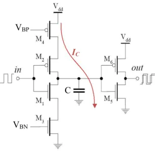
4.3.2 Charge Pump
For the MPPT circuit a Switch in drain Single-Ended Charge Pumps based in [22] was considered. This circuit (Figure 4-10) is the charge pump with the switch at the drain of the current mirror MOS. When the switch is turned off, the current pulls the drain of M1 to ground.
After the switch is turned on, the voltage at the drain of M1 increases from 0V to vdd. In the
mean time, M1 has to be in the linear region till the voltage at the drain of M1 is higher than the
minimum saturation voltage. During this time, high peak current is generated, even though the charge coupling is not considered. It is caused by the voltage difference of two series turn-on resistors from the current mirror, M1, and the switch. On the PMOS side, the same situation will
occur and the matching of this peak current is difficult since the amount of the peak current varies with the output voltage.
In Figure 4-7 the charge pump used in this work is shown and some modifications were made to the circuit above (Figure 4-10): a capacitor was added (C3) for biasing the rising/falling
time of the charge pump. A reset system was introduced, in order to always start the charge pump at 0V in this situation, discharging at this moment the capacitor C3. Additionally, some
connection was added to balance the IUP and IDW (Figure 4-10), i.e. to allow the system to have
the same speed time rising and falling.
Chapter 4 – Phase generation and control
35
Figure 4-10: Switch in drain single-ended charge pumps
4.4 Start-up circuit
The schematic of the start-up circuit is depicted in Figure 4-11. This circuit is based in [6], it shunts the input and the output nodes during the start-up of the circuit, guaranteeing that the phase controller circuit has a high enough power supply voltage to start working. This circuit also provides the reset signal, and its complement, for the ASM, the Charge Pump and some logical gates (XNOR and Flip-Flop type D).
1fF 45kΩ reset reset reset vdd vin vout 50 0.1x5 vdd vss 50 0.1x5 8 1 1 10
Chapter 4 – Phase generation and control
Chapter 5 – Simulation Results
37
Chapter 5
Simulation Results
All schematic capture and simulation of the circuits were performed using Cadence’s software (Spectre-Virtuoso®). To demonstrate the system operation, we designed the step-up converter using a standard 0.13 μm CMOS technology. All N-channel transistors used in this design have the bulk node connected to the ground (vss), and all P-channel transistors used in
this design have the bulk node connected to the positive potential (vdd).
The step-up converter was designed to work with a single amorphous solar cell, with an area of about 1 cm2, supplying a maximum power of 1775 μW and a MPP voltage of 403 mV,
in a standard 0.13 μm CMOS technology with VTN = 0.38 V and VTP = -0.33 V. The electrical model of the solar cell is described in chapter 2.
a) The MPPT behavior of the circuit under different light intensities
The first and second simulations of the system were carried out to verify the MPPT behavior of the circuit under different light intensities.
Chapter 5 – Simulation Results
38
Figure 5-1: Evolution of vin, vdd, vout and vVCO, during start-up and transient operation (Illumination of 100% and 17.5%, changing at 150μs)
In the first simulation, the value of the current IS in the solar cell model (Figure 2-1) was
changed from its maximum value (100%) to a lower value (17.5%) to simulate the change in illumination conditions. The value of the output capacitor of the circuit (Co) was limited to 10 nF due to simulation time restriction, this results in a large ripple in the output voltage. The behavior of the circuit, when the illumination changes from 100% to 17.5%, is shown in Figure 5-1.
This simulation shows that under a rapid reduction of the illumination level, the MPPT circuit is still capable of operating: even when the PV voltage is as low as 0.18V, the circuit is resulting in a local power supply voltage of only 0.57 V. This corresponds to the lowest illumination for which the circuit was capable of operating.
The second simulation was carried out for the system operating under different light intensities too, but in this case, the value of the current IS in the solar cell model (Figure 2-1)
was changed from a low value (19% of total illumination) to its maximum value (100%). The behavior of the circuit, when the illumination changes from 19% to 100%, is shown in Figure 5-2.
Chapter 5 – Simulation Results
39
Figure 5-2: Evolution of vin, vdd, vout and vVCO, during start-up and transient operation (Illumination of 19% and 100%, changing at 600μs)
The circuit is capable of starting-up with an illumination condition of 19% of maximum illumination and a load resistance of 1 kΩ, as show in Figure 5-2.
In Fig. 5-1 and 5-2 the relationship between the auto-tracked voltage (VVCO) and the
change in light intensity is shown. Under the same light intensity, the auto-tracked voltage (VVCO ) oscillates around the optimal value. When the light intensity changes, the MPPT circuit
adjusts the VVCO voltage level to the new optimal point.
b) The MPPT behavior of the circuit under different output resistor values
The third simulation was carried out to verify the MPPT behavior of the circuit under different output resistor values.
0 100 200 300 400 500 600 700 0 0.2 0.4 0.6 0.8 1 1.2 time (μs) In put , L oc al S up pl y, O ut put an d V C O co nt ro l vol ta ge s (V )
Output voltage(vout) Local supply voltage(vdd) Input voltage(vin)
Chapter 5 – Simulation Results
40
Figure 5-3: Evolution of vin, vdd, vout and vVCO, during start-up and transient operation (Illumination of 100% and load resistance changing at 250μs from 1 kΩ to 100Ω)
Like the Figure 5-3 shows, the circuit is capable of withstanding a change in the output resistor from 1 kΩ to 100 Ω.
To complete the study of the MPPT behavior of the circuit under the different output resistor values, the relevant parameters of the circuit for the different output resistor values were calculated for 100% of the illumination’s condition, using the time interval where the system behaviour was stable. These results are presented in Table 5-I.
In Table 5-I it is visible that: vout, vin, vdd and the frequency of the phases of the step-up
converter (at MPPT) increase with the increase of the output resistor; the ripple decreases with the increase of the output resistor; and the efficiency, Pout and Pin have the same curve’s shape
and they have the maximum points with an output resistor’s values between 750Ω and 1kΩ.
0 50 100 150 200 250 300 350 0 0.2 0.4 0.6 0.8 1 1.2 time (μs) Inpu t, L oc al S upp ly , O ut put a nd V C O c ont ro l vo lt ag es ( V ) vout vdd vin vVCO


![Figure 3-4: Schematic diagram of proposed MPPT using the RCC method [16]](https://thumb-eu.123doks.com/thumbv2/123dok_br/15595878.1051301/36.892.231.680.855.1090/figure-schematic-diagram-proposed-mppt-using-rcc-method.webp)