A FAMILY OF IMPROVED ZVT PWM CONVERTERS USING AN
AUXILIARY RESONANT SOURCE
M. L. Martins
∗H. Pinheiro
∗J. R. Pinheiro
∗H. A. Gr¨
undling
∗H. L. Hey
∗∗Power Electronics and Control Research Group - GEPOC, CT - Federal University of Santa Maria - UFSM
97105-900 - Santa Maria - RS - Brazil
ABSTRACT
This paper presents a novel family of Zero Voltage Tran-sition (ZVT) DC-DC PWM Converters that uses a reso-nant circuit as auxiliary commutation source to control the current through the auxiliary switch without addi-tional current stresses on main devices. The improved ZVT commutation cell enables the main switch to be turned on and off at Zero Voltage Switching (ZVS) and the auxiliary switch to be turned on and off at Zero Current Switching (ZCS) from zero to full-load.
KEYWORDS: DC-DC Converters, Zero-Voltage Transi-tion, Auxiliary Resonant Source.
RESUMO
Este trabalho apresenta uma nova fam´ılia de converso-res CC-CC PWM ZVT os quais utilizam um circuito ressonante como fonte auxiliar para controlar a corrente atrav´es da chave auxiliar sem agregar esfor¸cos adicio-nais de corrente nos dispositivos principais. A c´elula de comuta¸c˜ao aperfei¸coada possibilita a comuta¸c˜ao da chave principal sob tens˜ao nula e a comuta¸c˜ao da chave
Artigo submetido em 23/5/2002 1a. Revis˜ao em 7/2/2003
Aceito sob recomenda¸c˜ao do Ed. Assoc. Prof. Antonio M. N. Lima
auxiliar sob corrente nula desde carga nula at´e carga nominal.
PALAVRAS-CHAVE: Conversores CC-CC, Transi¸c˜ao Sob Tens˜ao Nula, Fonte Auxiliar Ressonante.
1
INTRODUCTION
Due to the current trend towards producing elec-tronic equipments with higher efficiency, power den-sity and EMI performance, the search for more efficient soft switching techniques becomes ever more intensive. Among these techniques, commutation at zero voltage -termed Zero Voltage Transition: ZVT - has often been used in low and medium power applications. This is be-cause of the low additional stresses added to the con-verter by the auxiliary commutation network located in parallel with the main power path, yielding low ad-ditional conduction losses when compared with other zero voltage switching techniques, Lee (1988) and Wang (1995).
Although ZVT is a well-accepted technique, several ZVT commutation cells proposed in the literature suffer draw-backs such as:
Hua (1992), Streit (1991);
• higher main switch current stresses, Yang (1993),
Moschopoulos (1995) and (1996), Smith (1997) and Tseng (1998);
• higher auxiliary switch voltage stresses, Yang
(1993) and Xu (2000);
• operation under limited voltage converter ratio,
Filho (1994);
• additional components count, Meneg´az (1999).
Among the ZVT commutation cell presented to date, the most attractive solution is presented by Martins (1993). However, it needs an autotransformer in the commuta-tion cell to perform the auxiliary commutacommuta-tion source, which may increase the size and complexity of the con-verter. In addition, the auxiliary switch is turned off with the magnetizing current.
This paper proposes an improved ZVT commutation cell that uses a resonant tank as auxiliary commuta-tion source, thereby eliminating some of the drawbacks mentioned above.
The paper is organized as follows: Section 2 introduces a family of Improved ZVT PWM DC-DC converters, and describes the operation principles of the improved ZVT boost converter. Section 3 sets out the soft com-mutation conditions. Section 4 gives a design guideline and presents an illustrative example. In Section 5 the feasibility of the proposed ZVT commutation cell is ver-ified by means of experimental results obtained from a prototype rated at 1 kW operating at 100 kHz. Finally, Section 6 sets out conclusions from the analysis and the results drawn.
2
PRINCIPLES OF OPERATION
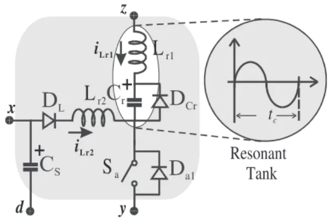
A new class of soft-switching converter was proposed by Hua (1992), namely ZVT PWM converters. These con-verters use a few additional elements placed in a parallel path with the main power circuit providing zero volt-age commutation for the main switch without additional voltage and current stresses. Thus, this approach over-came the main drawbacks presented by ZVS-QRC con-verters, Lee (1988), and ZVS-PWM concon-verters, Henze (1988). However, in Hua (1992) the auxiliary switch commutates with turn-on capacitive losses, reducing the overall efficiency gain and the EMI performance of these converters. To overcome these drawbacks this paper proposes an improved ZVT commutation cell shown in Fig. 1. It maintains the merits present in Hua (1992)
x
z
i
Lr2L
r1L
r2Resonant
Tank
t
c+
S
a+
y
d
i
Lr1Figure 1: Improved ZVT Auxiliary Commutation Cell.
and furthermore, achieves soft switching at zero current (ZCS) for auxiliary switch. To obtain these characteris-tics a resonant tank, which plays the role of the auxiliary source, is used to control the current through the auxil-iary switch. The resonant tank of Fig. 1 is represented by the inductor Lr1 and the capacitor Cr.
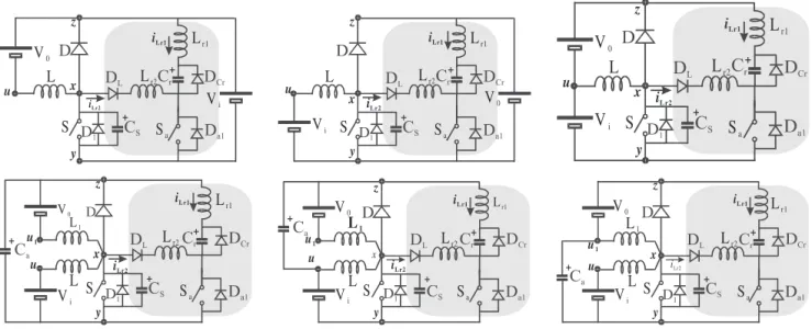
Fig. 2 shows a family of improved ZVT PWM DC-DC non-isolated converters obtained by incorporating the auxiliary resonant commutation cell to the common equivalent circuit of DC-DC converters presented by Irie (1990). It can be seen that the auxiliary commutation cell is placed in parallel with the main power path of each converter.
2.1
Operation Principles of Improved ZVT
Boost Converter.
To analyze the operation of the proposed improved ZVT DC- DC PWM converters, the improved ZVT PWM boost converter was chosen. Fig. 3 shows the simplified diagram for this converter. It differs from the boost converter presented in Fig. 2(b) in terms of the following assumptions used in the analysis:
• the input inductor is large enough to be considered
as a constant current sourceIduring one switching period;
• the output capacitor is large enough to be
consid-ered as a constant voltage sourceV0 ;
• all the semiconductors are considered ideal.
x z
u
iLr1
L Lr2
y S S a iLr2 + + V0 Vi Lr1 x z u
iLr1 Lr1
Lr2 y S S a iLr2 + + V0 Vi L x z u
iLr1
L
r1L
r2 yS
S
a iLr2 + +V
0V
iL
x z uiLr1 Lr1
Lr2
y
S Sa
iLr2 + + V0 Vi u1 + L L1 x z
iLr1 Lr1
Lr2 y Sa iLr2 + + + u S V0 Vi u1 L L1 x z
iLr1 L r1 Lr2 y Sa i Lr2 + + + u S V0 Vi u1 L L1
Figure 2: The Improved ZVT Family Converters.
Before the instant t0 the diode D is conducting the
in-put current I. The voltages across both switches are equal to the output converter voltage V0 and voltage
across auxiliary capacitor Cr is zero. The main
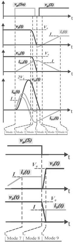
the-oretical waveforms during the main switch turn-on are presented in Fig. 4(a), whilst the turn-off and the PWM operation are presented in Fig. 4(b). The diagram of each circuit mode is presented in Fig. 5.
2.1.1 Mode 1. (t0, t1):
At t0, the auxiliary switch Sa is turned on and starts a
resonance process between iLr1(t) and vCr(t). At the
same time iLr2(t) begins to increase linearly until it
reaches the input current value. The voltage and current expressions to this mode are given by:
vCr(t) =V0−V0cos(ω1t), (1)
iLr1(t) =
V0
Z1
sin(ω1t) (2)
vCs(t) =V0 (3)
iLr2(t) = V0
Lr2
t (4)
The time interval of this mode is given by:
∆t1=t1−t0=
ILr2
V0
(5)
Where the impedance Z1is given by
Z1=
Lr1
Cr
(6)
and the resonant frequencyω1 by:
ω1=
1
√
Lr1Cr
(7)
2.1.2 Mode 2. (t1, t2):
When the current through Lr2 is equal to I, boost
diode D turns off and a resonant process begins between iLr2(t) current and vCs(t) voltage. This process will
completely discharge the energy stored into Cs. This
mode lasts until the current through the auxiliary switch reaches zero. The voltage and current behavior are given by the expressions:
vCr(t) =V0+ (VCr(t1)−V0) cos(ω1t)+
Z1ILr1(t1) sin(ω1t) (8)
iLr1(t) =
(V0−VCr(t1))
Z1
sin(ω1t) +ILr1(t1) cos(ω1t)
(9) vCs(t) =V0cos(ω2t) (10)
iLr2(t) =I+
V0
Z2
sin(ω2t) (11)
The time of this mode is given by:
∆t2=t2−t1=
π+ sin−1Z1
Z2
1 + 1 k1
ω1 −
IZ2
V0ω2
I
x
z
u
L
r1V
0L
r2
y
S
S
a
i
Lr1i
Lr2+
+
Figure 3: Improved ZVT Boost Converter.
where the impedanceZ2 is given by:
Z2=
Lr2
Cs
(13)
The resonant frequency is given by:
ω2=
1
√
Lr2Cs
(14)
The factork1 defines the ratio between the overcurrent
through inductor Lr2 defined as ∆I and the input
cur-rentI:
k1= ∆I/I (15)
2.1.3 Mode 3. (t2, t3):
During this mode, the auxiliary switch body diode Da1
turns on. This ensures the soft commutation conditions for the auxiliary switch turn-off. This circuit mode ends when the voltage vCs(t) reaches zero. The voltage and
current expressions to this mode are given by:
vCr(t) =V0+ (VCr(t2)−V0) cos(ω1.t)+
Z1ILr1(t2) sin(ω1t) (16)
iLr1(t) =(V0−VCr(t2))
Z1
sin(ω1t) +ILr1(t2) cos(ω1t)
(17) vCs(t) =V0cos(ω2t) +Z2(I−ILr2(t2))sin(ω2t) (18)
iLr2(t) =I+
V0
Z2
sin(ω2t) + (ILr2(t2)−I) cos(ω2t)
(19)
The time of this mode is given by:
∆t3=t3−t2=
π−2sin−1
Z1
Z2
1 + k11
ω1
(20)
Figure 4: Main theoretical waveforms: (a) Turn-on modes; (b) PWM and turn-off modes.
2.1.4 Mode 4. (t3, t4):
At t3, voltage vCs(t) reaches zero and the main switch
conditions for its turn-on with ZVS. At the same instant Da1turns off and the currentiLr2(t) decreases in a
res-onant fashion through Lr1, Lr2and Cr. This mode ends
whenvCr(t) reaches zero and the voltage boosting diode
DCr turns on. The voltage and current expressions to
this mode are given by:
vCr(t) =V0+ (VCr(t3)−V0) cos(ω3t)+
ILr1(t3) sin(ω3t) (21)
iLr1(t) = (VCr(t3)−V0)
Z3
sin(ω3t) +ILr1(t3) cos(ω3t)
(22)
vCs(t) = 0 (23)
iLr2(t) =−iLr1(t) (24)
The time of this mode is given by:
∆t4=t4−t3
=
sin−1Z1
Z2
1 + 1 k1
−tan−1
Z1ILr1(t4)
V0
+α
ω3
(25)
where the angle α is given in the Appendix.The impedanceZ3 is given by:
Z3=
Lr1+Lr2
Cr
(26)
and the resonant frequencyω3by:
ω3=
1
(Lr1+Lr2)Cr
(27)
2.1.5 Mode 5. (t4, t5):
At t4, the currents throughiLr2(t) andiLr1(t) decrease
linearly until it reachesI, when D1 is turned off. The
voltage and current expressions to this mode are given by:
vCr(t) = 0 (28)
iLr1(t) =
V0
Lr1+Lr2
t+ILr1(t4) (29)
vCs(t) = 0 (30)
iLr2(t) =−iLr1(t) (31)
The time of this mode is given by:
∆t5=t5−t4=
(I−ILr1(t4)) (Lr1+Lr2)
V0 (32) I x z u S y Lr1 V0 Lr2 Sa iLr1 iLr2 + + I x z y u S Lr1 V0 Lr2 Sa iLr1
iL r2
+ + I x z y u S Lr1 V0 Lr2 Sa iLr1 iLr2 + + I x z y u S Lr1 V0 Lr2 Sa iLr1 iLr2 + + I x z y u S Lr1 V0 Lr2 Sa iLr1 iLr2 + + I x z y u S Lr1 V0 Lr2 Sa iLr1
iL r 2
+ + I x z y u S Lr1 V0 Lr2 Sa iLr1
iL r2
+ + I x z y u S Lr1 V 0 Lr2 Sa iLr1 iLr2 + + I x z y u S Lr1 V 0 Lr2 Sa iLr1 iLr2 + +
Figure 5: The Improved ZVT Family Converters.
2.1.6 Mode 6. (t5, t6):
The current iLr2(t) continues to ramp down until it
reaches zero and the current through main switch S reaches I. In this mode, the expressions to the volt-ages and currents are the same as in Mode 5. The time of this mode is given by:
∆t6=t6−t5=
ILr1(t5) (Lr1+Lr2)
V0 (33)
2.1.7 Mode 7. (t6, t7):
2.1.8 Mode 8. (t7, t8):
At t7, the main switch S is turned off and the currentI
is diverted to the snubber capacitor Csand its voltage is
linearly charged up to output converter voltageV0. The
voltage and current expressions to this mode are given by:
vCr(t) = 0 (34)
iLr1(t) = 0 (35)
vCs(t) =
I Cs
t (36)
iLr2(t) = 0 (37)
The time of this mode is given by:
∆t8=t8−t7=
CsV0
I (38)
2.1.9 Mode 9. (t8, t9):
WhenvCs(t) voltage reachesV0, the boost diode D turns
on, and another switching cycle begins.
3
SOFT COMMUTATION CONDITIONS
3.1
Main switch turn-off (ZVS)
As described in Mode 8 of Section 2, after main switch S is turned off, the input current is diverted from switch to a snubber capacitor Cs. As a result, voltage across the
main switch increases with controlled dv/dt achieving zero voltage turn-off. The capacitance value is given by expression (39) as follows:
Cs=
I tf
2ksV0
(39)
where tf is the fall time of the semiconductor device
used and factorksis chosen to reduce the commutation
energy dissipated by the semiconductor. The range of ksis defined below:
0< ks<1 (40)
3.2
Main switch turn-on (ZVS/ZCS)
To achieve main switch turn-on without losses, it is ini-tially necessary to divert the input current from boost diode D to inductance Lr2 and after, to discharge
com-pletely the snubber capacitor Cs. This way the
reso-nant process betweeniLr2(t) andvCs(t) must lasts until
vCs(t) achieves zero. This condition is assured by the
following expression:
ω1=
2k1ω2
2π−sin−1
Z1
Z2
1 +k11
(2 +k1π)
(41)
3.3
Auxiliary switch turn-on (ZCS)
As described in Modes 1 and 2 of Section II, by the pres-ence of inductors Lr1and Lr2current through auxiliary
switch Sa increases with controlleddi/dt achieving zero
current turn-on. Furthermore, by an appropriate choice of Lr2, the reverse-recovery losses of boost diode D can
be minimized. The expression (42) can be used to choose the inductanceLr2:
Lr2>
V0
d dtiD
(42)
where d
dtiDis the turn-off di/dt rate of the boost diode.
3.4
Auxiliary switch turn-off (ZCS/ZVS)
To assure the conduction of diode Da1, ensuring the
aux-iliary switch turn-off without losses, the following re-lation between the characteristics impedances must be satisfied:
Z1
Z2
= k1
k2(1 +k1)
(43)
where the constant k2 must be greater than one and
is defined as the ratio between the maximum values of current through each one of the resonant inductors Lr1
and Lr2 as shown below:
k2=
ILr1(max)
ILr2(max)
>1 (44)
4
DESIGN GUIDELINES
This section describes a design procedure and gives an example of how to determine the component values of the proposed improved ZVT PWM boost converter.
The input data are defined as follows:
• Output Power: P0= 1000W
• Output Voltage: V0= 400V
• Operation Frequency: fs = 100 kHz
• Minimum estimate efficiency: η >95 %
The design guidelines consist of the following eleven steps:
1. The value of the capacitance Cscan be determined
by a turn-off capacitive snubber procedure as pre-sented by Mohan (1995). However, to minimize the number of auxiliary components, in this example, Cs is adopted as the intrinsic output capacitance
of the semiconductor device (MOSFET – IRP450). Thus, Cs is defined as: Cs=Coss= 0.4nF
2. From the output power and the minimum estimate efficiency, the input power is defined: Pi = Pη0 =
1050W
3. From the input power and the input voltage, the input current is defined by: I= Pi
Vi = 7.0A
4. The inductance Lr2is obtained from the expression
(48) where the factor k1 is chosen as equal to k1
=0.25. Lr2=Ck2s 1
V0
I
2
= 22.15µH
5. The impedance Z2 is calculated by: Z2=
Lr2
Cs =
235.3 Ω
6. The resonant frequencyω2 is calculated by: ω2 = 1
√
Lr2Cs = 10.62M rad/s
7. To ensure ZCS commutation to switch Sa, k2 is
defined by (44) and was chosen equal tok2 = 1.1:
8. Substitutingk2andk1values in expression (43), the
impedance Z1 is given by: Z1= 42.79 Ω
9. From the expression (41),ω1is: ω1= 9.8M rad/s
10. The inductance of the resonant tank is given by: Lr1=Zω11 = 4.36µH
11. The capacitance of the resonant tank is given by: Cr= Z11ω1 = 2.38nF
5
EXPERIMENTAL RESULTS
Following the design example shown in Section 4, a 100 kHz, 1 kW improved ZVT PWM boost converter proto-type has been implemented to verify the operation and the performance of the proposed improved ZVT com-mutation cell. The power circuit operates from a 150 V DC voltage source and supplies a 400V resistive load as shown in Fig. 6. Its main parameters are summarized in
S
D
Sa L
DL
DCr Lr1
Cr Vi
C R Lr2
MUR1560
RHRP8120
HGTP7N60C3D IRFP450
MUR1560
UF5406 1N5352 Ls
Figure 6: Improved ZVT Auxiliary Commutation Cell.
Table 1: Experimental Parameters
Component Parameter
Vi (input voltage) 150 V
V0 (output voltage) 400 V
P0 (output power) 1.0 kW
fs (switching frequency) 100 kHz
L (input filter) 0.91 mH
C (output filter) 150 uF
S (main switch) IRFP450
Sa (auxiliary switch) HGTP7N60C3D
D (boost diode) MUR1560
DL (blocking diode) MUR1560
Db (auxiliary diode) RHRP8120
Lr1 (resonant inductor) 3.5µH
Lr2 (resonant inductor) 21.7µH
Cs (resonant capacitor) 400 pF (Cs= Coss)
Cr (resonant capacitor) 3.0 nF (= 2 x 1.5 nF)
Table I. The main switch used was IRFP450 (MOSFET) and the auxiliary switch used was HGTP7N60C3D (600 V, 7 A) UFS (Ultra Fast Switches) series IGBT from Intersil Semiconductors, which present a built-in, anti-parallel hyperfast diode. To reduce the auxiliary semi-conductors parasitic capacitance effects in the auxiliary circuit, a saturable reactor implemented with 8 turns on a Toshiba “spike killer” core (SA14x8x4.5) was used, as well as a clamped circuit represented by the dashed lines in the power stage circuit diagram, Fig. 6.
As can be seen in Fig. 7(a), the gate-source signal of switch S, is applied only after the voltagevDS reaches
zero, characterizing the zero voltage turn-on.
con-ditions achieved to auxiliary switch permit the use of minority carrier devices which are more appropriate for these conditions. As a result, the turn-on capacitive losses presented by the ZVT converters proposed in Hua (1992), Streit (1991) and Meneg´az (1999) are consider-ably reduced.
Fig. 7(c) shows the voltage across the resonant capacitor Crand the current through resonant inductors Lr1and
Lr2.
Figure 8 shows the measured efficiency of the boost converter with the improved ZVT commutation cell as function of the output power, whose value was approx-imately equal to 96.5% at full load (1 kW). For com-parison purposes, Fig. 11 also includes the efficiency curves of the conventional ZVT boost converter, Hua (1992), and its hard-switching counterpart. The mea-sured efficiencies at full load were, respectively, 96.1% and 94.3%. Using the resonant tank, the ZCS condi-tions are achieved to the auxiliary switch, so that the turn-on capacitive losses presented in Hua (1992) are avoided, ensuring an efficiency gain by the proposed con-verter for high load conditions. As the tank energy is proportional to the converter voltage output V0, the
cir-culating reactive energy is maintained almost constant for whole load range, which mitigates the efficiency gain obtained with the auxiliary switch ZCS operation at low load conditions.
6
CONCLUSIONS
A family of Improved ZVT PWM converters is pre-sented. These converters retain the merits of ZVT pro-posed by Hua (1992): namely, neither voltage nor cur-rent stress on main devices, and low additional conduc-tion losses when compared to its PWM counterpart. Furthermore, soft switching at zero current (ZCS) for the auxiliary switch is achieved, which is more suitable for minority carrier devices, allowing the reduction of converter switching losses.
To obtain these characteristics without the presence of a DC voltage source in the auxiliary circuit, a resonant tank is used as auxiliary commutation source. It con-trols the current flux between main power and auxiliar circuits. In addition, it also controls the current through the auxiliary switch without additional current stresses on main switch as presented in Yang (1993), Moschopou-los (1995, 1996), Smith (1997) and Tseng (1998).
Operating principles and commutation process are de-scribed and verified by experimental results, which were obtained from a prototype of 1 kW operating at 100 kHz,
(a) Main Switch: Ch1 - vDS(t), Ch2 -vGS(t).
(b) Auxiliary Switch: Ch1 - vCE(t), Ch2 - vGE(t),Ch3 - iC(t).
(c) Resonant Elements: Ch1 vCr(t), Ch3 - iLr1(t), Ch4 - iLr2(t), Time=250 ns/div.
Figure 7: Experimental results.
P
0(W)V=150V V=400V
i 0
Improved ZVT Conventional ZVT Hard-switching
Figure 8: Converters efficiencies.
ACKNOWLEDGMENT
The authors would like to express their special thanks to
Thornton Inpec Eletrˆonica Ltda and Icotron – an
EP-COS Company and Toshiba do Brasil S.A. for material
support.
A
APPENDIX
The angleαis defined by the expression below:
α=α1−α2+α3 (45)
where:
α1=sin−1
Z
1
Z2
1 + 1 k1
(46)
α2=tg−1
Z
1ILr1(t4)
V0
(47)
α3=sin−1
(Z3−Z1) (1 +k1)I cos
π
2 −α1
cos (α2) tan
π
2 −α1
(48)
REFERENCES
Filho, N. P., Farias, V. J. and Freitas, L. C. (1994). A Novel Family of DC-DC PWM Converters Us-ing the Self-resonant Principle. Proc. of the 25th
Power Electronics Specialists Conference PESC’94,
pp. 1385-1391.
Henze, C. P., Martin H. C. and Parsley, D. W. (1988). Zero-Voltage-switching in High Frequency Power Converters Using Pulse Width Modulation. Proc. of the 3rd Conference on Applied Power
Electron-ics and Exposition APEC’88, pp. 33-44.
Hua, G.; Leu, C. and Lee, F. C (1992). Novel Zero-Voltage Transition PWM Converters. Proc. of the 23th Power Electronics Specialists Conference
PESC’92, pp. 55-60.
Irie, H. (1990) Resonant Switches in Common Equiv-alent Circuit of DC/DC Converters. Proc. of the 2nd International Power Electronics Conference
IPEC’90,pp. 362-368.
Lee, F. C. (1988). High-frequency Quasi-resonant Con-verter Topologies. Proc. of the IEEE, Vol.76, No. 4, pp. 377-390.
Martins, D. C.; Seixas, F. J.; Barbi, I. and Brilhante, J. A. (1993). A Family of DC-to-DC PWM Convert-ers Using a New ZVS Commutation Cell. Proc. of the 24th Power Electronics Specialists Conference
PESC’93, pp. 524-530.
Meneg´az, P. J. M.; C´o, M. A.; Simonetti, F. C and Vieira, J. L. F. (1999). Improving the Operation of ZVT DC-DC Converters.Proc. of the 30th Power
Electronics Specialists Conference PESC’99, pp.
293-297.
Mohan, N.; Undeland, T. M. and Robbins, W. P. (1995). Power Electronics - Converters, Applications and Design. 2˚Ed., John Wiley & Sons, NY.
Moschopoulos, G.; Jain, P. and Joos, G. (1995). A Novel Zero-Voltage Switched PWM Boost Con-verter.Proc. of the 26th Power Electronics
Special-ists Conference PESC’95, pp. 694-700.
Moschopoulos, G.; Jain, P.; Joos, G. and Liu, Y. (1996). A Zero-Voltage Switched PWM Boost Converter With na Energy Feedforward Auxiliary Circuit.
Proc. of the 27th Power Electronics Specialists
Con-ference PESC’96, pp. 76-82.
Streit, R. and Tollik, (1991), A High Efficiency Telecom Rectifier Using A Novel Soft-switched Boost-based Input Current Shaper. Proc. of the 13th
Telecom-munication Energy Conference INTELEC’91, pp.
720-726.
Smith, K. M. and Smedley, K. M. (1997). A Comparison of Voltage-Mode Soft-switching Methods for PWM Converters. Trans. on Power Electronics, Vol. 12, no. 2, pp. 376
−386.
Tseng, C. and Chen, C. (1998). Novel ZVT-PWM Con-verters With Active Snubbers. Trans. on Power
Wang, K., Hua, G. and Chen, C. (1995). Analysis, De-sign and Experimental Results of ZCS-PWM Boost Converters. Proc. of the 3rd International Power
Electronics Conference IPEC’95, pp. 1197-1202.
Xu, D. M.; Zhang, J. M.; Ren, Y. C. and Qian, Z. (2000). A Novel Single-phase Active-clamped ZVT-PWM Converter. Proc. of the 15th Conference on
Ap-plied Power Electronics and Exposition APEC’00,
pp. 456-459.
Yang, L. and Lee, C. Q. (1993). Analysis and Design of Zero-Voltage Transition PWM Converter.Proc. of the 8th Conference on Applied Power Electronics