Universidade de Aveiro 2014
Departamento de Eletrónica, Telecomunicações e Informática
João Paulo Sá
da Silva
PROCESSAMENTO DE DADOS EM ZYNQ APSoC
Universidade de Aveiro 2014
Departamento de Eletrónica, Telecomunicações e Informática
João Paulo Sá
da Silva
PROCESSAMENTO DE DADOS EM ZYNQ APSoC
DATA PROCESSING IN ZYNQ APSoC
Dissertação apresentada à Universidade de Aveiro para cumprimento dos requisitos necessários à obtenção do grau de Mestre em Engenharia de Computadores e Telemática, realizada sob a orientação científica do Prof. Dr. Valeri Skliarov, Professor Catedrático do Departamento de Eletrónica, Telecomunicações e Informática da Universidade de Aveiro e da Prof.ª Dr.ª Iouliia Skliarova, Professora Auxiliar do Departamento de Eletrónica, Telecomunicações e Informática da Universidade de Aveiro.
o júri
presidente Prof. Doutor Joaquim João Estrela Ribeiro Silvestre Madeira Professor Auxiliar da Universidade de Aveiro
Prof. Doutor Hélio Sousa Mendonça
Professor Auxiliar da Universidade do Porto (arguente)
Prof. Doutor Valeri Skliarov
agradecimentos Começo por agradecer aos meus orientadores Prof. Doutor Valeri Skliarov e Prof. Doutora Iouliia Skliarova pelo acompanhamento, encorajamento, rigor exigido e pela liberdade que me permitiram.
Também quero agradecer a todos os que fizeram parte desta jornada que agora termina e de alguma forma contribuíram para o seu sucesso.
palavras-chave FPGA,Sistemas Digitais Reconfiguraveis, Processadores,
Co-processadores, Sistemas Embutidos, Co-desenvolvimento Hardware e Software,Peso de Hamming, Ordenação de Dados, Acelerador de Software, Custo de Comunicações, Interfaces de Alto Desempenho.
resumo Field-Programmable Gate Arrays (FPGAs) foram inventadas pela Xilinx em 1985, ou seja, há menos de 30 anos. A influência das FPGAs está a crescer continua e rapidamente em muitos ramos de engenharia. Há varias razões para esta evolução, as mais importantes são a sua capacidade de reconfiguração inerente e os baixos custos de desenvolvimento.
Os micro-chips mais recentes baseados em FPGAs combinam capacidades de software e hardware através da incorporação de processadores multi-core e lógica reconfigurável permitindo o desenvolvimento de sistemas computacionais altamente otimizados para uma grande variedade de aplicações práticas, incluindo computação de alto desempenho, processamento de dados, de sinal e imagem, sistemas embutidos, e muitos outros.
Neste contexto, este trabalho tem como o objetivo principal estudar estes novos micro-chips, nomeadamente a família Zynq-7000, para encontrar as melhores formas de potenciar as vantagens deste sistema usando casos de estudo como ordenação de dados e cálculo do peso de Hamming para vetores longos.
keywords FPGA, Reconfigurable Digital Systems, Processors, Co-processors, Embedded Systems, Hardware and Software Co-design, Hamming Weight, Data Sorting, Software Accelerator, Communication
Overheads, High-Performance Ports.
abstract Field-Programmable Gate Arrays (FPGAs) were invented by Xilinx in 1985, i.e. less than 30 years ago. The influence of FPGAs on many directions in engineering is growing continuously and rapidly. There are many reasons for such progress and the most important are the inherent reconfigurability of FPGAs and relatively cheap development cost.
Recent field-configurable micro-chips combine the capabilities of software and hardware by incorporating multi-core processors and reconfigurable logic enabling the development of highly optimized computational systems for a vast variety of practical applications, including high-performance computing, data, signal and image processing, embedded systems, and many others.
In this context, the main goals of the thesis are to study the new micro-chips, namely the Zynq-7000 family and to apply them to two selected case studies: data sort and Hamming weight calculation for long vectors.
i
Contents
1. Introduction ... 1 1.1. Motivation ... 1 1.2. Related Work... 2 1.3. Outline ... 4 1.4. Prototyping Systems ... 5 1.5. Development Tools ... 10 1.5.1 Vivado ... 101.5.2 Software Development Kit ... 12
2. Methods and Tools for On-chip Interactions between Hardware and Software Modules 13 2.1. Introduction ... 13
2.2. Programmable Logic ... 14
2.2.1 GP-PS Master ... 14
2.2.2 AXI_HP & AXI_ACP ... 16
2.2.3 LogiCORE IP AXI Master Lite... 16
2.2.4 LogiCORE IP AXI Master Burst ... 18
2.2.5 Final Remarks ... 20
2.3. Processing System ... 20
2.3.1 Standalone ... 21
2.3.2 Linux ... 21
2.3.3 Other Modes ... 22
3. Hardware/Software Co-design for Data Sort ... 23
3.1. Introduction ... 23
3.2. Methods, Motivations, and Related Work ... 24
3.3. Hardware Software Architectures ... 27
3.3.1 A Single Core Implementation ... 29
3.3.2 A Single Core Implementation with Parallel Operations ... 30
3.3.3 A Multi-Core (a Dual-Core) Implementation ... 31
3.3.4 A Multi-Core (a Dual-Core) Implementation with Parallel Operations ... 31
3.4. Experiments and Comparisons ... 33
3.4.1 Experimental Setup ... 33
3.4.2 Experimental Comparison of Software only and Hardware Software Sorters ... 35
3.4.3 Discussion of the Results ... 39
3.5. Conclusion ... 40
ii
4.1. Introduction ... 41
4.2. Related Work... 42
4.3. Highly Parallel Circuits for Popcount Computations ... 42
4.4. System Architecture ... 43
4.5. Design and Evaluation of FPGA-based Accelerators ... 47
4.6. Design and Evaluation of APSoC-based Accelerators ... 50
4.7. Discussion of the Results ... 55
4.8. Conclusion ... 56
5. Conclusions and Future Work ... 57
5.1. Conclusions ... 57
5.2. Future Work ... 57
5.2.1 Hardware / Software Co-design outside of Zynq ... 57
5.2.2 Three Tier Hardware / Software Co-design ... 58
5.3. Publications ... 58
iii
List of Figures
Figure 1.1 Interactions between the basic functional components of the Zynq-7000 APSoC .... 5
Figure 1.2 The simplified layout of ZedBoard ... 8
Figure 1.3 Settings for configuring the ZedBoard: from flash memory (a), from JTAG (b), from SD card (c) ... 8
Figure 1.4 The simplified layout of ZyBo ... 9
Figure 1.5 Windows on the screen in Vivado design suite ... 11
Figure 2.1 Interfaces for PS – PL Communication from [16] ... 13
Figure 2.2 General interface between the PS and the PL ... 15
Figure 2.3 General links between the VHDL modules ... 15
Figure 2.4 Top-level diagram ... 16
Figure 2.5 Component diagram for Data Processing top module and FSM in Data Processor module ... 17
Figure 2.6 Component diagram for a sort project using AXI Master Lite ... 18
Figure 2.7 Component diagram and FSM for Data Processing Top Module ... 19
Figure 2.8 Component diagram for a sorting project using the AXI Master Burst ... 20
Figure 3.1 The basic architecture of hardware/software data sorter ... 26
Figure 3.2 Potential parallel operations in APSoC ... 27
Figure 3.3 Hardware/software architecture for a single core implementation ... 29
Figure 3.4 Hardware/software architecture for a dual core implementation ... 30
Figure 3.5 Functions of different threads in a multi-core implementation ... 32
Figure 3.6 Hardware/software architecture for a dual core implementation ... 33
Figure 3.7 Experimental setup ... 34
Figure 3.8 The results of projects for architectures proposed in sections 3.3.1-3.3.4 ... 39
Figure 4.1 FPGA-based accelerator for general-purpose computer. ... 44
Figure 4.2 APSoC-based accelerator for general-purpose computer. ... 45
Figure 4.3 Interactions between the basic functional components in the Zynq-7000 APSoC. .. 46
Figure 4.4 The proposed architecture for popcount computations in an FPGA-based accelerator. ... 48
Figure 4.5 An example of popcount computations for N=256 and =32. ... 48
Figure 4.6 General structure of the project. ... 51
Figure 4.7 Popcount computations in the PL reading data through 4 high-performance ports in burst mode. ... 52
Figure 4.8 Post implementation resources for Table 6 from the Vivado 2014.1 report (FF – flip-flops, LUT – look-up tables, Memory LUT – LUTs used as memories, BUFG – Xilinx buffers). . 54
iv
Figure 4.9 Popcount computations for using 5 AXI ports in burst mode. ... 55
List of Tables
Table 3.1 The results of experiments with one block of size N data items in software only,
hardware/software and hardware only ... 36
Table 3.2 The results of experiments for N=256 (ZedBoard) and different values of L (from 29=512 to 226=33,554,432 data items) ... 37 Table 3.3 The results of experiments similar to the Table 2 but architecture from section 3.3.2 is used for the projects ... 38 Table 3.4 The results of experiments similar to the Table 2 but architecture from section 3.3.3 is used for the projects ... 38 Table 3.5 The results of experiments similar to the Table 2 but architecture from section 3.3.4 is used for the projects ... 38 Table 4.1 The Results of Experiments (=32) ... 49 Table 4.2 The Results of Experiments (data are transferred through one 32-bit ACP high-performance port and =32) ... 53
Table 4.3 The Results of Experiments (data are transferred through one 64-bit ACP high-performance port and =64) ... 53
Table 4.4 The Results of Experiments (data are transmitted through four 32-bit high-performance ports and =32) ... 53
Table 4.5 The Results of Experiments (data are transmitted through four 64-bit high-performance ports and =64) ... 53
Table 4.6 The Results of Experiments (data are transmitted through four 32-bit high-performance ports and one 64-bit ACP) ... 53 Table 4.7 The Results of Experiments (data are transmitted through four 64-bit high-performance ports and one 64-bit ACP) ... 53
v
Abbreviations:
ACP – Accelerator Coherency Port
APSoC – All Programmable System-on-Chip APU – Application Processor Unit
ARM – Advanced RISC Machine
ASCII – American Standard Code for Information Interchange ASIC – Application Specific Integrated Circuit
ASSP – Application Specific Standard Product AXI – Advanced eXtensible Interface
BSP – Board Support Package CE – Chip Enable
CHWC – Combinational Hamming Weight Counter CLB – Configurable Logic Block
CPU – Central Processing Unit CS – Chip Select
DDR – Double Data Rate DMA – Direct Memory Access DSP – Digital Signal Processing DTC – Device Tree Compiler
ELF – Executable and Linkable Format EMIO – extended MIO
FA – Full Adder
FIFO – First In, First Out
FPGA – Field-Programmable Gate Array FSBL – First Stage Boot Loader
FSM – Finite State Machine GCD – Greatest Common Divisor GP – General Purpose
GPIO – General Purpose Input Output GPU – Graphics Processing Unit GUI – Graphical User Interface
HDL – Hardware Description Language HDMI – High-Definition Multimedia Interface HLS – High-Level Synthesis HP – High-Performance HS – Horizontal Synchronization HW – Hamming Weight I/O – Input/Output II – Initiation Interval
ILA – Integrated Logic Analyzer IP – Intellectual Property
IPIC – Intellectual Property Interconnect IPIF – Intellectual Property Interface ISE – Integrated Software Environment JTAG – Joint Test Action Group LED – Light-Emitting Diode LSB – Least Significant Bit LUT – Look-Up Table
LVCMOS – Low Voltage Complementary Metal Oxide Semiconductor MIO – Multiplexed Input/Output
vi OLED – Organic Light-Emitting Diode
OS – Operating System OTG – On The Go PC – Personal Computer
PHFSM – Parallel Hierarchical FSM PL – Programmable Logic
POPCNT – Population Count PS – Processing System Pmod – Peripheral Module QSPI – Quad-SPI
RAM – Random-Access Memory RF – Radio Frequency
RTL – Register Transfer Level SD – Secure Digital
SDK – Software Development Kit SPI - Serial Peripheral Interface SoC – System-on-Chip
TCL – Tool Command Language TSM – Trigger State Machine
UART – Universal Asynchronous Receiver/Transmitter UCF – User Constraints File
USB – Universal Serial Bus UUT – Unit Under Test VCNT – Vector Count Set Bits VGA – Video Graphics Array
VHDL – VHSIC Hardware Description Language VHSIC – Very High Speed Integrated Circuits VS – Vertical Synchronization
XADC – Xilinx Analog to Digital Converter XDC – Xilinx Design Constraints
XMD – Xilinx Microprocessor Debugger XPS – Xilinx Platform Studio
1
1.
Introduction
Field-Programmable Gate Arrays (FPGAs) were invented by Xilinx in 1985, i.e. less than 30 years ago. The influence of FPGAs on many directions in engineering is growing continuously and rapidly. There are many reasons for such progress and the most important are the inherent configurability of FPGAs and relatively cheap development cost. Forecasts suggest that the impact of FPGAs will continue to grow and the range of applications will increase considerably in future. Recent field-configurable micro-chips combine the capabilities of software and hardware by incorporating multi-core processors and reconfigurable logic appended with a number of frequently used devices such as digital signal processing slices and block memories. Such integration leads to the creation of complex programmable systems-on-chip allowing fixed plus variable structure multi-core computational systems to be built. Xilinx Zynq-7000 all programmable system-on-chip (APSoC) can be seen as a new and efficient way to integrate on a chip the most advanced reconfigurable devices and a widely used processing system based on the dual-core ARM CortexTM MPCoreTM. There are now very efficient computer-aided design systems available (e.g. Xilinx Vivado). There are also high-performance interfaces between the processing system and the reconfigurable logic that are supported by ready-to-use intellectual property cores. These, combined with numerous architectural and technological advances, have enabled APSoCs to open a new era in the development of highly optimized computational systems for a vast variety of practical applications, including high-performance computing, data, signal and image processing, embedded systems, and many others.
1.1. Motivation
A system-on-chip (SoC) contains the necessary components (such as processing units, peripheral interfaces, memory, clocking circuits and input/output) for a complete system. The Xilinx Zynq-7000 family features the first All Programmable System-on-Chip - APSoC architecture that combines the dual-core ARM CortexTM MPCoreTM-based processing system (PS) and Xilinx programmable logic (PL) on the same microchip. APSoC permits functionality of the components and communications between them to be changed using the software tools provided by Xilinx [1] therefore orienting it to each user unique needs.
The Zynq APSoC enables implementation of custom logic in the PL and custom software in the PS. This means offering the flexibility and scalability of an FPGA while featuring performance, power, and ease of use typically associated with Application Specific Integrated Circuits (ASIC) and Application Specific Standard Products (ASSP). Each Zynq-7000 device contains the same
2
Processing System, however the Programmable Logic and IO resources vary ensuring that the diverse target designs constrains are met with the most adequate hardware. It allows for the realization of unique problem-oriented systems in such areas as [2]:
• Automotive driver assistance, driver information, and infotainment • Broadcast camera
• Industrial motor control, industrial networking, and machine vision • IP and Smart camera
• LTE radio and baseband
• Medical diagnostics and imaging • Multifunction printers
• Video and night vision equipment
The integration of the PS with the PL allows levels of performance that two-chip solutions (e.g., an ASSP with an FPGA) cannot match due to their limited I/O bandwidth, latency, and power budgets [2].Given these advantages, it is important to find the best ways to use the platform enabling the maximum potential to be achieved. This is the main target of this thesis.
1.2. Related Work
The Zynq family attracts many researchers. Two books [1], [3], one of them being co-authored by the author of this thesis, and several papers within this area have been published in English. The books focus mainly on teaching how to use the platform while the papers provide interesting results on specific topics.
The current state-of-the-art Next Generation Sequencing (NGS) computing machines are lowering the cost and increasing the throughput of DNA sequencing. The paper [4] proposes a practical study that uses a Zynq board to summarize acceleration engines using FPGA accelerators and ARM processors for the state-of-the-art short read mapping approaches. The experimental results show speed up of more than 112 times and the potential to use accelerators in other generic large scale big data applications.
LINQits [5] is a flexible hardware template that can be mapped onto programmable logic for a mobile device or server. LINQits accelerates a domain-specific query language called LINQ. LINQits is prototyped in ZYNQ with improved energy efficiency in a factor from 8.9 to 30.6 and performance in a factor from 10.7 to 38.1 compared to optimized, multithreaded C programs running on conventional ARM A9 processors.
3
Multi-rotor Unmanned Aerial Vehicles (UAVs) are attractive for both commercial and private use. Simple tasks like aerial photography are widely known and used, but new applications are gaining importance like on-board video processing or complex sensor data utilization. These scenarios require high-performance on-board processing which is not available in most of today's avionics architectures for civilian multi-rotor systems. Fundamental requirements on the architecture and flight control algorithms of existing autonomously flying commercial multi-rotor UAVs are presented in [6] where a new avionics architecture using the Xilinx Zynq platform is proposed.
Computer networks also benefit from Zynq as show in [7] with implementation of an OpenFlow switch on a Zynq board. The results show that the design targeted can achieve a total 88 Gbps throughput for a 1K flow table which supports dynamic updates. Correct operation has been demonstrated using a ZC706 board [8]. The architecture is divided on a high-performance, yet highly-programmable, data plane processing residing in the programmable logic, while complex control software runs in ARM processing system.
The best way to communicate between the PS and PL has also been object of study in [9]. In this paper several Zynq interfaces are tested in several scenarios and a detailed practical comparison of the speed and energy efficiency of various PS-PL memory sharing techniques is done.
Microsoft’s project Catapult [10] for accelerating the Bing Search Engine data centre combines the server rack computers and FPGAs achieving, under high load, a significant improvement on the ranking throughput of each server. This example does not use the Zynq technology, but it is a case where such technology could be used very successfully especially because it is optimised for interactions between software and hardware.
Besides the academic research several projects using Zynq have appeared:
GNU Radio [11], many of the needed signal processing blocks are implemented in the PL taking advantage of the FPGA capacity to support broad parallelism
FreeRTOS [12], the free real time operating system is now available for the Zynq platform
Bit coin mining [13] provides an efficient Bitcoin miner implemented through high-level synthesis
4
1.3. Outline
Chapter one is the introduction providing information on the motivation and background on the platform used. At the beginning a brief overview of APSoC is presented and advantages of this platform are discussed. Then applications of Zynq both in academic and educational research are considered. Finally both the prototyping systems and the coding tools are described with some detail with references to further study.
Chapter two describes platform-specific features regarding communication and operating system capabilities. The first part focuses on the PL and interface types explaining how each port can be used and how relevant IP cores can be chosen. The second part focuses on the PS considering two modes of operation: under Linux operating system or Standalone (Bare-Metal) and describes how each interface can be used.
Chapter three is dedicated to the sorting problem and studies the applicability of the Zynq platform taking advantages of hardware/software co-design. Central points of chapter three are:
1. Hardware/software partitioning for processing large sets of data that is based on sorting networks in hardware and merging in software.
2. Merging techniques in software based on single-core and multi-core (dual-core) implementations for Zynq APSoCs.
3. The use of high-performance and general-purpose ports in Zynq APSoCs.
4. The results of thorough experiments and comparisons for sorting large data sets in two Zynq APSoC-based prototyping systems: ZyBo from Digilent [14]and ZedBoard [15] from Avnet.
Chapter four explores the Popcount problem solving it in the Zynq platform and includes the following topics:
1. New highly parallel methods for popcount computations in FPGA-based systems which are faster than existing alternatives.
2. A hardware/software co-design technique implemented and tested in APSoC from the Xilinx Zynq-7000 family.
3. Data exchange between software and hardware modules through high-performance interfaces in such a way that the implemented burst mode enables run-time popcounts computations to be combined with data transactions.
4. The result of experiments and comparisons demonstrating increase of throughput comparing to the best known hardware and software implementations.
5
The last chapter, five, presents an overall conclusion about the developed projects and future work.
1.4. Prototyping Systems
Figure 1.1 illustrates interactions between the basic functional components of the Zynq-7000 APSoC [16] that contains two major top-level blocks: the processing system and the programmable logic. Communications with external devices are provided through multiplexed input/outputs (MIO) with potential extension from the PL through extended MIO (EMIO).
Application Processor Unit (dual-core
ARM)
PL to memory interconnect
High-performance ports
Central
Interconnect
General-purpose ports
Clocks ResetI/O
Me
mo
ry
in
te
rf
ac
es
M u lt ip le xe d Inp u t/ Ou tp u t (M IO)Ex
te
n
d
ed
MIO
(
EMIO
)
In
te
rr
u
p
ts
DMA
Interrupts
PS
PL
Acce le ra to r co h er en cy p o rt ( A CP )Arrow lines show port
control from master
to slave
Configurable logic cells
Block RAM
DSP slices
12-bit analog to digital
converters (XADC)
Data can flow in both
directions through
the ports
DMA OCM CacheMemory
interfaces
O C MB
A
C
Figure 1.1 Interactions between the basic functional components of the Zynq-7000 APSoC
The application processor unit (APU) contains two ARM Neon engines with dedicated and shared cache memories, static dual-port RAM, registers, and controllers. A snoop controller enables access to the cache memories and on-chip memories (OCM) from the PL through an accelerator coherency port (ACP). There are two levels of cache: 32 KB (level L1) independent for each engine (central processing unit - CPU) and 512 KB (level L2) shared by both engines (CPUs). Two 32 KB caches of the level L1 are available for each CPU: one for instructions (I-cache) and
6
one for data (D-cache). The DMA controller has four channels for the PS, four channels for the PL and enables access to/from any memory to be provided in the system. An interrupt controller handles different types of events including interrupts from the PL.
The Zynq has multi-stage boot process that includes the factory-programmed (inaccessible by users) boot ROM and the first stage boot loader (FSBL) initializing automatically the APSoC after a system reset from the selected external boot device, such as JTAG, flash memory or SD card. The boot ROM checks the relevant mode registers and executes subsequent configuration steps specified in the FSBL [16] reading the images from the indicated boot device (SD card, flash memory or JTAG).
Features and capabilities of the PS are comprehensively described in [16]. The PL provides features available for Artix-7/Kintex-7 FPGA and contains:
Digital signal processing (DSP) slices DSP48E1 providing arithmetical and bitwise operations on up to 48-bit operands and some additional functionality;
36 Kb dual-port block RAM up to 72 bits wide;
Clock managers;
Dual 12-bit Xilinx Analog to Digital Converter (XADC);
Configurable inputs and outputs;
Additional components for Kintex devices.
There are a number of functional interfaces between the PS and PL that include Advanced eXtensible Interface (AXI) interconnect, EMIO, interrupts, DMA and debug. The AXI interconnect contains:
o One 64-bit master port (AXI_ACP port) in the PL (see A in Figure 1.1) allowing coherent access from the PL to the cache (level L2), and on-chip memories – OCM in APU of the PS.
o Four high-performance master ports (AXI_HP ports) in the PL (see B in Figure 1.1) providing 32-bit or 64-bit independently programmed data transfers. They are optimized for high bandwidth access from the PL to external DDR and OCM memories [17].
o Four general-purpose ports (AXI_GP ports) two of which are 32-bit master interfaces and the other two – 32-bit slave interfaces (see C in Figure 1.1). They are optimized for access from the PL to the PS peripherals and from the PS to the PL registers/memories [17].
7
There are many details about Zynq microchips that are not covered here and can be found in the comprehensive Xilinx technical reference manual [16].
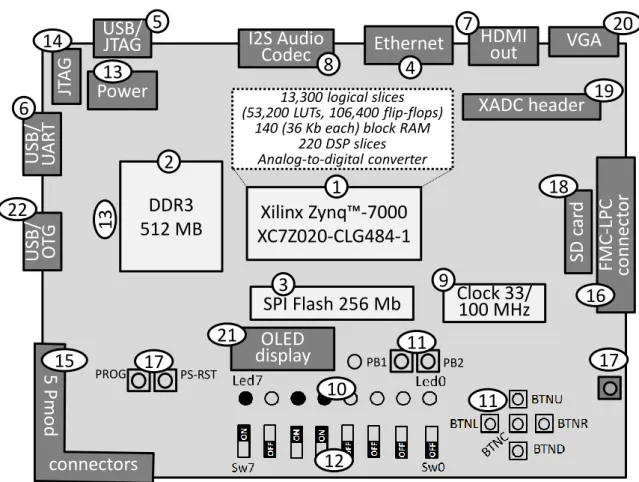
Prototyping in Zynq-based boards (such as [14], [15], [18]) is considered to be the base for verifying the described projects. Mainly the designed circuits and systems will be implemented in Zynq microchips available on ZedBoard [15] and ZyBo [14] including one xc7z020clg484 (Zed) or xc7z010clg400 (ZyBo) APSoC of Zynq 7000 family with embedded dual-core Cortex-A9 PS and PL based on Artix-7 FPGA. The ZedBoard has the following main components and connectors (see Figure 1.2):
1. Xilinx Zynq™-7000 APSoC xc7z020-1clg484c (some details about the PL section are given in Figure 1.2 in a dashed rectangle).
2. 512 MB DDR3 memory with 32-bit wide data.
3. 256 Mb 4-bit SPI (Quad-SPI) Flash for initialization of the PS (16 Mb), configuration of the PL and data storage.
4. 10/100/1000 Ethernet.
5. Onboard USB-JTAG programming.
6. USB-UART (Universal Asynchronous Receiver/Transmitter) port. 7. HDMI (High-Definition Multimedia Interface) output.
8. I2S Audio Codec (audio line-in, line-out, headphone, microphone). 9. 33.3 MHz clock source for the PS and 100 MHz oscillator for the PL. 10. 9 user LEDs (1 LED on the PS side and 8 LEDs on the PL side).
11. 7 user buttons for GPIO - General-Purpose Input/Output (2 buttons on the PS side and 5 buttons on the PL side).
12. 8 slide switches.
13. Power connector and power-on LED indicator. 14. 2×7 programming JTAG connector.
15. 5 Pmod expansion connectors (26).
16. FMC-LPC (FPGA Mezzanine Card -Low Pin Count) connector (68 single-ended or 34 differential I/Os).
17. Two reset buttons.
18. SD (Secure Digital) card slot. 19. XADC header.
20. VGA (Video Graphics Array) connector.
21. 128x32 OLED (Organic Light-Emitting Diode) display. 22. USB 2.0 OTG (On The Go) plug.
8
Xilinx Zynq™-7000
XC7Z020-CLG484-1
1
I2S Audio
Codec
8
HDMI
out
7
Ethernet
4
SPI Flash 256 Mb
3
DDR3
512 MB
2
Clock 33/
100 MHz
9
Power
13
JT
A
G
14
FMC
-L
PC
co
n
n
ec
to
r
16
17
11
12
10
US
B/
U
A
R
T
6
PB1 PB211
13
7
5
Pmo
d
connectors
15
PROG17
PS-RSTSD
car
d
18
XADC header
19
VGA
20
OLED
display
21
USB/
JTAG
5
US
B/
O
TG
22
13,300 logical slices (53,200 LUTs, 106,400 flip-flops)140 (36 Kb each) block RAM 220 DSP slices Analog-to-digital converter
Figure 1.2 The simplified layout of ZedBoard
The Zynq microchip on the ZedBoard can be configured using: Quad-SPI, SD Card or JTAG. The onboard jumpers (not shown in Figure 1.2) permit the required configuration mode to be selected (see Figure 1.3). Five mode pins are used to indicate the boot source [16]. Figure 1.3 shows settings in the ZedBoard for the mode pins used in this book for selecting configuration from Quad SPI flash (Figure 1.3a), JTAG (Figure 1.3b), and SD card (Figure 1.3c).
a)
b)
c)
Figure 1.3 Settings for configuring the ZedBoard: from flash memory (a), from JTAG (b), from SD card
(c)
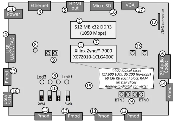
The ZyBo board (based on the smallest member of the Xilinx 7000 family) has the following main components and connectors (see Figure 1.4):
9
1. Xilinx Zynq™-7000 APSoC xc7z010-1clg400C (some details about the PL section are given in Figure 1.4 in a dashed rectangle).
2. 512 MB (x32) DDR3 memory (with 1050 Mb per second bandwidth). 3. 10/100/1000 Ethernet.
4. Shared UART/JTAG USB port. 5. HDMI port.
6. Audio codec connectors.
7. 50 MHz clock to the PS (allowing the processor to be operated at a maximum frequency 650 MHz) and external 125 MHz clock to the PL (the details are given in [5]).
8. 5 user LEDs (1 LED on the PS side and 4 LEDs on the PL side).
9. 6 user buttons for GPIO (2 buttons on the PS side and 4 buttons on the PL side). 10. 4 slide switches.
11. Power connector. 12. JTAG connector.
13. 5 Pmod expansion connectors (26), including 3 high-speed Pmods. 14. XADC (analog) Pmod.
15. Two reset buttons. 16. Micro SD card slot. 17. VGA connector. 18. USB OTG connector.
19. 128 Mb serial flash with QSPI interface.
Xilinx Zynq™-7000 XC7Z010-1CLG400C 1 512 MB x32 DDR3 (1050 Mbps) 2 7 9 9 12 15 19 Sw3 8 10 Led3 BTN0 BTN3 Ethernet 3 US B U A R T/ JT A G 4 HDMI out 5 I2S A u d io Co d ec 6 8 Power11 Pm o d 13 Pmod 13
Pmod Pmod Pmod
13 13 13 Pm o d 14 Micro SD 16 VGA 17 US B/ O TG 18 JT A G c o n n e ct o r 4,400 logical slices (17,600 LUTs, 35,200 flip-flops)
60 (36 Kb each) block RAM 80 DSP slices Analog-to-digital converter
10
The Zynq microchip on the ZyBo can be configured using: Quad-SPI, micro SD card or JTAG. The onboard jumpers JP5 (not shown in Figure 1.4) permit the required configuration mode to be selected [14] much like it is done for the ZedBoard.
1.5. Development Tools
The Xilinx Vivado Design Suite can be used to develop software and hardware. Two main components of the Vivado are IP Integrator and Software Development Kit (SDK). The IP Integrator is an IP and system-centric design environment targeted to the Xilinx 7th series FPGAs and APSoCs. It is used to describe the hardware in VHDL (or Verilog), synthesize, implement and configure FPGA or APSoC. It also offers the possibility of design simulation and run-time verification (with ILA – Integrated Logic Analyser). The Software Development Kit (SDK), based on Eclipse, is used to write C/C++ code for the PS section of APSoC.
1.5.1 Vivado
Vivado is an IP and system-centric design environment targeted to the Xilinx 7th series FPGAs and APSoCs. The detailed information, design guides, and tutorials are available at the Xilinx website. Here just the minimal details are presented that are needed to introduce the tool and the proposed methods. The Vivado design suite integrates tools available separately in the previous Xilinx software.
When Vivado is launched many different options may be chosen. A new project will be of RTL (Register Transfer Level) type and may include existing hardware description language files, IP cores, simulation sources, and constraints. If a new project is created then several windows appear on the screen (see Figure 1.5). Described below are just a few options and introductory design steps.
Options available in the flow navigator (shown on the left-hand side of Figure 1.5) are synthesis, implementation and generating bitstream, analysis, and simulation as well as in-circuit verification and debug. The menus (File … Help) in the upper part integrate numerous options that may be chosen in different design scenarios: to work with files and projects; to execute different steps for the design flow (that are also shown on the left hand side of Figure 1.5); to change project settings; to open existing IP cores and templates; and some others comprehensively explained in the relevant documentation available from Xilinx.
11
Note that options in different menus depend on the currently chosen design scenario. For example, the described above options in the File menu are valid when a project is open in the Vivado and they are different when working on an elaborated design (from the menu on the left-hand side of Figure 1.5). Thus, the menus are context-dependent and the given above examples are chosen just because they are used more often. Let us now briefly characterize the remaining windows in Figure 1.5 that permit:
to observe project structure (hierarchy), check libraries and work with the templates providing assistance in using hardware description language constructions and frequently needed circuits;
to analyze opened designs;
to verify waveforms with the aid of the integrated simulator;
to debug run-time designs using the integrated logic analyzer (ILA);
to check messages about warnings and errors;
to execute numerous additional scenarios that are outside of the scope of the thesis and can be found in manuals and tutorials from Xilinx.
Menu
Flow
Navigator
Project Manager Project Settings Add Sources IP Catalog IP IntegratorCreate Block Design Open Block Design Generate Block Design Simulation
Simulation Settings Run Simulation RTL Analisys
Open Elaborated Design Synthesis
Synthesis Settings Run Synthesis
Open Synthesized Design Implementation
Implementation Settings Run Implementation Open Implemented Design Program and Debug
Bitstream Settings Generate Bitstream Open Hardware Manager Launch iMPACT
File Edit Flow Tools Window Layout View Help
Project Manager
Sources (hierarchy, libraries, compile order) and templatesPreview
Properties
Project
TCL console,
Messages, Log,
Reports, Design Runs
Figure 1.5 Windows on the screen in Vivado design suite
12
1.5.2 Software Development Kit
The Xilinx SDK provides a full environment for building software applications for Xilinx embedded processors (soft and hard). It comes with the GNU-based compiler toolchain (GCC compiler, GDB debugger, utilities, and libraries), JTAG debugger, flash programmer, drivers for Xilinx IPs and bare-metal board support packages, middleware libraries for application-specific functions, and an IDE for C/C++ bare-metal and Linux application development and debugging. SDK is based upon the open source Eclipse platform and incorporates the C/C++ Development Toolkit (CDT). Features include [20]:
• C/C++ code editor and compilation environment • Project management
• Application-build configuration and automatic makefile generation • Error navigation
• Integrated environment for debugging and profiling embedded targets
• Additional functionality available using third-party plug-ins, including source code version control
The SDK also includes a template for creating a First Stage Bootloader (FSBL) and a graphical interface for building a boot image. The SDK can be launched from Vivado when exporting a new hardware definition.
The Xilinx Microprocessor Debugger (XMD), also included in SDK, is a JTAG debugger that can be invoked on the command line to download, debug, and verify programs. It includes a Tool Command Language (Tcl) interface that supports scripting for repetitive or complex tasks. XMD is not a source-level debugger, but serves as the GDB server for GDB and SDK when debugging bare-metal applications. When debugging Linux applications, SDK interacts with a GDB server running on the target. Debuggers can connect to XMD running on the same host computer or on a remote host on the network.
13
2.
Methods and Tools for On-chip Interactions between
Hardware and Software Modules
2.1. Introduction
The major advantage and novelty of the Zynq is the hardcore CPU tightly coupled with an FPGA on the same chip, the APSoC. To take advantage of such setup it is necessary to understand how the two entities (PS & PL) that compose the platform may communicate in order to work in a collaborative manner. Otherwise we would just be wasting recourses and the Zynq would not be the ideal choice for the job. The APSoC has 9 interfaces that permit communication between the PS and PL; these interfaces have already been mentioned in the previous chapter and are now going to be detailed. Figure 2.1 from [16] shows such interfaces along some other information.
Figure 2.1 Interfaces for PS – PL Communication from [16]
In first row of the table, GP – PS Slave allows the PL to interact as Master directly with several components available in the PS. This interface does not have much interest in the software hardware co-design area and was not explored. Additional details about it are available in [16].
GP – PS Master, is the interface in the second row, it permits direct data exchange between the PS and the PL. In these transactions the PS is always the master, which means it always initiates transactions either by sending data to the PL or by requesting data from the PL. This interface can be used in one of two ways: 1) IO controlled by CPU, or 2) through DMA available in the PS side. The CPU programmed IO is the method that offers the worst throughput but consumes the smallest recourses (DMA controllers are limited) and also it is the simplest to use. It is suggested in [16] that programmed IO is used for control functions and DMAs for other data transfers. Programmed IO is extensively used as suggested and its importance will be shown later on.
The last two rows represent the interfaces for indirect data transfer. PS and PL exchange data through an external passive agent, a memory (the On-Chip Memory or the DDR), here both the PS
14
and the PL act as Masters of the shared memory, being both capable of initiating data transfers. These interfaces offer the best throughput. The main difference between the AXI_HP and AXI_ACP interfaces is where they are connected, see Figure 1.1, AXI_HP ports are connected to the “PL to Memory Interconnect” while the AXI_ACP port is connected directly to the APU. This configuration ensures that accessing data in the shared memories through the AXI_ACP interface has the same Quality of Service (QoS) as the Processing Cores in the APU achieving the lowest possible latency and having optional cache coherency. The advantages of this interface must be used with caution as it shares the processing cores bandwidth, possibly lowering their performance and also large bursts of data may cause thrashing of the cache. This interface is meant for small data transfers (conditioned to the cache size) and to off-load the processing cores work to a specialized co-processor implemented in the PL. On the other hand, the AXI_HP interface is meant to be used in larger data transfers.
Using indirect communication offers a much higher throughput but also introduces a new problem: the need for signalling mechanisms, to avoid the waste of resources in polling operations. For signalling from the PS to the PL the aforementioned GP – PS Master Interface fits perfectly, allowing not only for signalling but also sending specific control information such as data start address in memory, data size and even operation to realize. For the reverse signalling it is not possible to use the GP – PL master interface, but the traditional signalling mechanism for peripherals to the CPU, interruptions, is available. In this case, when the PL needs to signal the PS, for example to request more data or to indicate that an operation has completed, it asserts the interrupt line. The PS in the Interrupt Service Routine reads a specific register in the PL, through the GP – PS master Interface, and acts accordingly. All topics in this chapter can be further studied with explanations and examples provided in [21].
2.2. Programmable Logic
2.2.1 GP-PS Master
In this thesis the GP port is mainly used for control functions, therefore its utilization example will be based in such interactions. Xilinx provides a very useful IP Core to handle this interface abstracting the AXI protocol details and supporting point-to-point bidirectional data transfers, the relevant IP Core is LogiCORE IP AXI4-Lite IPIF [22]. At the moment of this writing the latest version is v2.0.
15
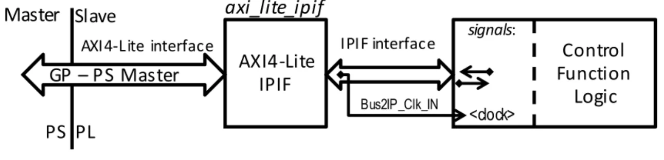
AXI4-Lite interface IPIF interface
PS PL
GP – PS Master
Master
Slave
AXI4-Lite
IPIF
Control
Function
Logic
signals: Bus2IP_Clk_IN <clock>axi_lite_ipif
Figure 2.2 General interface between the PS and the PL
There are three groups of signals in the interface: 1) system signals establishing interaction with the PS through general-purpose input/output (GPIO) ports (through the AXI4-Lite IPIF); 2) system clock/reset signals; 3) user signals for interactions with the control functions. Signals from the first group are processed by the Xilinx IP core axi_lite_ipif. Signals from the third group are handled in control logic module that is shown in Figure 2.3 in a simplified form including structural connections and fragments of VHDL code.
-- Definition of the top-level component
entity GPIO_Control is port( -- signals of AXI Slave Interface
--signals to control other modules in the PL );
end GPIO_Control;
architecture RTL of GPIO_Control is
-- Constants for generic map supplying generic parameters to the Xilinx axi_lite_ipif component
begin
-- instantiation of the developed control module -- instantiation of the Xilinx axi_lite_ipif module
end RTL;
entity GPIO_LOGIC is port ( );
end GPIO_LOGIC;
architecture Behavioral of GPIO_LOGIC is
-- declaration of constants and signals
begin
-- Control Functions
end Behavioral;
entity axi_lite_ipif is -- this is the Xilinx axi_lite_ipif entity generic (….);
port ( );
end axi_lite_ipif;
architecture imp of axi_lite_ipif is
-- this is Xilinx architecture that enables communications -- through the chosen general-purpose port to be -- established
end imp;
16
The Xilinx LogiCORE IP AXI4-Lite IP Interface (IPIF) [22] is optimized for slave operations and does not provide support for direct memory access (DMA) and master services. The IPIF creates a set of signals allowing interactions with AXI4-lite bus to be easily understood. If the name of a signal begins with Bus then the signal comes from the bus and goes to the user module. Otherwise, the signal goes from the user module to the bus.
Finally, it is worth noting that the Xilinx IP Core axi_lite_ipif provides an addressing mechanism based on address spaces that relieves the developers of address filtering by using a more convenient approach based on Chip Enable/Select and Write/Read Enable signals, examples of this as well the rest of this interface usage are available at http://sweet.ua.pt/skl/TUT2014.html.
2.2.2 AXI_HP & AXI_ACP
Although the interfaces are different they share the same protocol. Xilinx provides IP Cores to abstract these interfaces, they are the LogiCORE IP AXI Master Lite [23] and the LogiCORE IP AXI Master Burst [24]. The main difference between these two IP Core is that the Lite version implements just a subset of the AXI protocol (AXI-Lite) thus being simpler to use, less resource consuming but does not allow burst transfers.
When using indirect communication, the GP – PS Master Interface is used for control functions, retrieving the status of the Data Processing Module and providing the signal to the interrupt line. This separates the control from data transfers enabling an easier understanding of the design. Figure 2.4 shows a general top level diagram for this type of communication.
Data Processing Module
AXI_HP or AXI_ACP GP – PS Master
Control Module Control
Status Interrupt Line
Figure 2.4 Top-level diagram
2.2.3 LogiCORE IP AXI Master Lite
At the moment of this writing the latest version of this core is v3.0. The Data Processing Module using the lite protocol is shown in figure 2.5.
17
init
read
proc
write
done
Reading data R ea di ng is comp le te d P roc essi n g is com p le te d Sorting data Writing results Jobis completed Initializing
The Data Processor entity
Xilinx
axi_master_lite
component
Data Processing Top Module
Figure 2.5 Component diagram for Data Processing top module and FSM in Data Processor module
The Data processor component includes an FSM with state transition diagram shown in Figure 2.5. The FSM provides support for read/write memory operations through AXI ports and controls data processing. There are four states in the FSM and they are responsible for the following operations:
The state init is the first FSM state which initializes internal signals with data received from the control module.
In the state read data items are sequentially received from the selected memory area. Depending on the chosen address mapping, we can use either DDR or OCM. As soon as all items have been received, transition to the state proc is executed.
The state proc activates the Data Processor component. This may be a sorting processor using, for example, iterative even-odd-transition network that tests when sorting is completed (see the enable signal in [25], [26]). As soon as sorting is completed, transition to the state write is carried out.
In the state write data items are sequentially written to the selected memory area. Dependently on the chosen address mapping, we can use either DDR or OCM. As soon as all items have been written, the transition to the state done is performed.
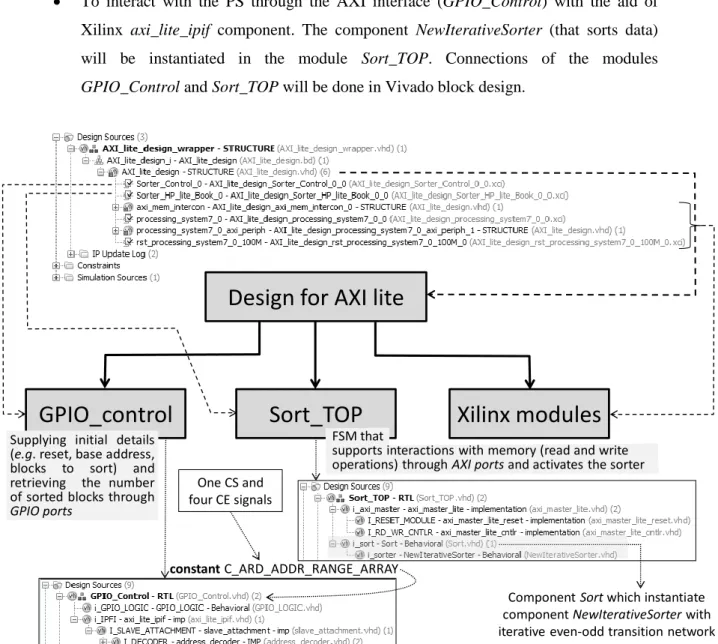
The state done indicates that the job has been completed.
A component diagram for a sorting project using AXI Master Lite is presented figure 2.6 as an example. The top module instantiates several components, two of which are GPIO_Control and Sort_TOP. The remaining components are Xilinx IP cores supporting AXI-lite interactions. The
18
main functions of the components GPIO_Control and Sort_TOP are (more details on sorting are presented in chapter 3):
To sort data in hardware (Sort_TOP) with an iterative even-odd transition network
To interact with the PS through the AXI interface (GPIO_Control) with the aid of Xilinx axi_lite_ipif component. The component NewIterativeSorter (that sorts data) will be instantiated in the module Sort_TOP. Connections of the modules GPIO_Control and Sort_TOP will be done in Vivado block design.
Sort_TOP
Design for AXI lite
GPIO_control
Xilinx modules
Component Sort which instantiate component NewIterativeSorter with iterative even-odd transition network
constant C_ARD_ADDR_RANGE_ARRAY
One CS and four CE signals Supplying initial details
(e.g. reset, base address, blocks to sort) and retrieving the number of sorted blocks through GPIO ports
FSM that
supports interactions with memory (read and write operations) through AXI ports and activates the sorter
Figure 2.6 Component diagram for a sort project using AXI Master Lite
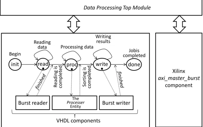
2.2.4 LogiCORE IP AXI Master Burst
At the moment of this writing the latest version of this core is v2.0. Much like the previously presented IP Core, the AXI Master Burst allows the same strategy to be implemented but this mode is more complex. The suggested approach is to divide the read and write states presented in figure 2.6 in modules with their own state machine to specifically handle the burst read/write and generate signals finished as soon as reading/writing is completed and thus transition to the next state can be done. Figure 2.7 presents necessary illustrations.
19
init
read
proc
write
done
Reading data R ea ding is com ple te d So rting is comple te d Processing data Writing results Jobis completed Begin The Processer Entity
Burst reader
Burst writer
VHDL components
Xilinx
axi_master_burst
component
Data Processing Top Module
The NewIterativeSorter entity
Figure 2.7 Component diagram and FSM for Data Processing Top Module
The component diagram for a sorting project using the AXI Master Burst is depicted in Figure 2.8. The top module instantiates several components, two of which are GPIO_Control and Sort_TOP. The remaining components are Xilinx IP cores. The main difference with the previous section is in two new components in the module Sort that are BurstRead and BurstWrite that execute burst read/write and generate signals finished as soon as reading/writing is completed and thus transition to the next state can be done. Besides, the Xilinx component axi_master_lite in Figure 2.6 has been replaced with the Xilinx component axi_master_burst.
20
Sort_TOP
Design for AXI lite
GPIO_Control
Xilinx modules
Component Sort which instantiates components
NewIterativeSorter, BurstRead and BurstWrite
with the iterative even-odd transition network
FSM with 6 states: init, requestRead, waitAck, burstRead, waitCmdCmpt, done FSM with 6 states: init, requestWrite, waitAck, burstWrite, waitCmdCmpt, done
FSM and components (NewIterativeSorter, BurstRead,
BurstWrite) can also be described in form of a
hierarchical finite state machine (see [20] for details)
Design Libraries
Design Libraries
FSMs that
support interaction with memory and activate the sorter
Figure 2.8 Component diagram for a sorting project using the AXI Master Burst
2.2.5 Final Remarks
All interfaces can be used directly without the Xilinx IP Core, which may reduce the design resource overhead and increase the maximum attainable frequency but forces the developer to handle manually the AXI interface increasing development time. Note, that the Xilinx IP Cores will be maintained by Xilinx avoiding potential problems in the future. These arguments should be taken into consideration when deciding how to handle communication in a new system.
Complete projects for all the examples are available online at
http://sweet.ua.pt/skl/TUT2014.html .
2.3. Processing System
Communication from the PS Perspective works in two ways either send/receive data directly to/from the PL using the GP – PS Master Interface or store data in the memory to be later accessed by the PL. Implementation varies depending on the mode in use. Both Linux and Standalone have advantages and disadvantages.
21
2.3.1 Standalone
Standalone is the simplest mode enabling C compiled code to be run directly in the ARM processor, i.e., without any software layer between them. This mode is used when only a main loop and a few other tasks, which can be encapsulated in interrupts, are required. It is also very useful for testing.
Sending and receiving data using the GP – PS Master is easily achieved by accessing a pre-assigned memory address range, defined in [16]. For indirect communications, a fixed address range defined at design time can be used. Another option is dynamically defined memory ranges, using the memory allocation primitives available and then sending the assigned start address and size of intended memory areas through the GP-PS Master Interface. This latter option relieves the programmer of some of the responsibility of memory management. Finally keep in mind that when using AXI_HP or AXI_ACP with coherency disable it is mandatory to guaranty that the data to be retrieved by the PL is not in CPU Cache to ensure correct results. When using ACP with coherency enable this problem does not exist. Regarding the usage of interrupts, several interrupt handlers can be defined one for each interrupt line available.
2.3.2 Linux
Linux mode offers the standard OS abstractions such as Virtual Memory, Multiprogramming, File system, Inter Process Communication, Hardware abstraction, etc. These advantages came at the price of increased overhead and development time. This mode is used when there are needs for several independent tasks to run at the same time, possibly sharing resources.
For interaction with the PL, contrasting with the Standalone mode, a more complex methodology is required. In the traditional way the developer has to hack the kernel to include a driver for the PL device. Considering that most of the time all that is needed is to provide access to the PL memory space and handle an interrupt line this may seem too much effort. To address this situation, the userspace I/O system (UIO) was designed by the Linux kernel developers. In this document all interactions using Linux will be based in the UIO.
To use UIO a set of steps are required, starting with adding an entry to the device tree file representing the PL and containing the required address spaces and interrupt lines used. Note that now fixed address spaces must be used for both the direct and indirect communications. This step allows for the creation of a special device file “/dev/uioX” that can be mapped in a process address space to access the PL.
22
As a final note, it is possible to access the memory directly through the special file “/dev/mem” in the same way it is done in the Standalone mode. This possibility requires super user permissions, is very unsafe and can cause system instability.
2.3.3 Other Modes
The two modes presented above are the most commonly used, but a few other modes are also available and can be consulted in [27].
23
3.
Hardware/Software Co-design for Data Sort
3.1. Introduction
Sorting is a procedure that is needed in numerous computing systems [28]. For many practical applications, sorting throughput is very important. To keep up with increasing performance requirements, fast accelerators based on FPGAs (e.g.[29]–[37]), GPUs (e.g. [33], [38]–[42]) and multi-core CPUs (e.g.[43], [44]), have been investigated in depth with multiplied intensity during the last few years. The former can be explained by the recent major advances in high-density and high performance microelectronic devices that have originated serious challengers to general-purpose and application-specific processing systems for solving computationally intensive problems. The results are especially promising if multiple operations can be executed simultaneously. Two of the most frequently investigated parallel sorters are based on sorting [29] and linear [30] networks. A sorting network is a set of vertical lines composed of comparators that can swap data to change their positions in the input multi-item vector. The data propagates through the lines from left to right to produce the sorted multi-item vector on the outputs of the rightmost vertical line.
It is shown in [26] that the fastest known even-odd merge and bitonic merge circuits are very resource consuming and can only be used effectively in existing FPGAs for sorting very small data sets. An alternative solution is based on an iterative even-odd transition network that is very regular and can be implemented very efficiently in FPGAs for larger data sets. Besides, for many practical applications the effective throughput is higher than in other known networks (e.g. [29], [30]), which is demonstrated in [26] on results of numerous experiments in FPGA. The size of blocks (sub-sets of data) sorted in FPGA is increased but it is still small and constrained by the available FPGA resources. The best scenario would be to sort tens of millions of data items while using significantly cheap microchips. Thus, the problem has been split into two parts [26], [35], one executed in reconfigurable logic and the other in software running on embedded high-performance processors. Zynq APSoCs are very appropriate for such decomposition. The following steps [26] have been applied:
1. A large set of data is divided into such subsets that can be sorted in APSoC PL with the aid of iterative networks [26].
2. The subsets are stored in memory accessible from both APSoC PS and the PL.
3. The PL reads each data subset from the memory, sorts it using the iterative network, and copies the sorted subset back to the memory, in a sequential fashion.
24
4. The PS reads the sorted subsets from the memory and merges them producing the final result of sorting.
Processing data in the PL is very similar to [26] and this is not the target of this chapter. The central points of interest are:
How efficiently the methods [26] can be used for sorting large data sets based on subsequent merging in software of sorted in hardware sub-sets.
Study and evaluation of different types of parallelism for data sort.
Study and evaluation of communication overheads and effectiveness of available high-performance interface AXI Accelerator Coherency Port for Zynq microchips [16].
How the size of the blocks [26] influences on effective throughput of data sorters.
Exact comparison of software only and hardware/software sorters for large data sets.
The remainder of the chapter is organized in 4 main sections. Section 3.2 presents the main ideas of the proposed method and motivations. Section 3.3 discusses software/hardware architectures and suggests methods to parallelize computations and to increase throughput. Section 3.4 presents the experimental setup, discusses experiments in APSoCs, and comparisons. Conclusion is given in section 3.5.
3.2. Methods, Motivations, and Related Work
Performance is critical for the majority of computational systems in which sorting plays an important role. From the analysis presented in [26] the following can be taken:
1. The known even-odd merge and bitonic merge circuits are the fastest and they enable the best throughput to be achieved. However, they are very resource consuming and can only be used effectively in existing FPGAs for sorting very small data sets.
2. Pipelined solutions permit even faster circuits than in point 1 to be designed. Usually pipelining can be based on flip-flops in FPGA slices used for the network and resource consumption is more or less the same as in point 1. Once again, in practice, only very small data sets can be sorted in FPGAs.
3. To use even-odd merge and bitonic merge circuits for large data sets, the following two methods are the most commonly applied: a) large data sets are sorted in host computers/processors based on sorted subsets of the large sets produced by an FPGA (see, for example, [29], [35]); b) the sorting networks for large sets are segmented in such a way that any segment can be processed easily and the results from the processing are handled sequentially to form the sorted set (see, for example, [31], [39]). Both methods involve intensive communications, either between an FPGA
25
and a host computing system/external memory (the size of memory embedded to FPGA is limited), or between a processing system (such as [39]) and memory.
4. The existing even-odd merge and bitonic merge circuits are not very regular (compared to the even-odd transition network for example) and, thus the routing overhead may be considerable in FPGAs.
5. It is shown that very regular even-odd transition networks with two sequentially reusable vertical lines of comparators are more practical because they operate with a higher clock frequency, provide sufficient throughput, and enable a significantly larger number of items to be sorted in the same PL. Further, a pipeline can be constructed [26] if required allowing a compromise between the performance and resources to be found.
6. Experiments done in [21], [25] give additional motivation to the methods [26] which finally have been chosen for implementation of sorting networks in reconfigurable logic (in the PL) of APSoC.
Note that although some non-essential modifications have been done in the method [26] all the ideas and circuits are very similar. The most related work to the described here methods can be found in [26], [28]–[44] and it was profoundly discussed in [25], [26].
Fig. 3.1 outlines the basic architecture of hardware/software data sorters that will be considered in this chapter.
The following four designs will be analysed:
1. A single core implementation where software in the PS and hardware in the PL operate sequentially. Analysis of such implementation permits communication overheads to be easily found.
2. A single core implementation where software in the PS and hardware in the PL operate in parallel. It permits further comparisons with multi-core solutions to be done. Different cores frequently share the same memory which leads to performance degradation and the latter needs to be evaluated.
3. A dual-core implementation where software in the PS and hardware in the PL operate sequentially. This permits to compare dual-core and single-core solutions taking into account communication overheads between software and hardware.
4. A dual-core implementation where software in the PS and hardware in the PL operate in parallel which allows the highest level of parallelism to be examined.
26
R
eg
is
te
r
(R
)
0
7
1
2
3
4
5
6
1
2
3
4
5
6
clock clock enableenable = 1 if there is at least
one data swap in the second vertical line of comparators,
else enable = 0 Data item
Data item Comparator /swapper Data item Comparator /swapper
Even
Odd
Signals from all odd and even
comparators participate in forming the enable signal
PL
Merge
Merge
Merge
Merge
Merge
PS
Sorted set
Zynq APSoC
Me
m
o
ry
:
ext
ern
al
DDR,
o
n
-ch
ip
-m
em
o
ry
(OC
M)
o
r
cach
e
Sorted
sub-sets (blocks)
Figure 3.1 The basic architecture of hardware/software data sorter
Access to memories can be done in lite and burst modes. The latter is faster [21] especially for transferring large data sets and it will be used in all the proposed designs. Fig. 3.2 demonstrates the highest level of parallelism. Note that some advanced microchips available in more expensive prototyping boards (e.g. [8]) allow communications with higher level systems (such as a host PC) through PCI-express. Thus, additional level of parallelism may be involved: the first level is software of the host PC; the second level is software of the PS and the third level is hardware of the PL. This topic is planned for future work.
Note that higher parallelism requires more sophisticated interactions between processing units that execute parallel operations. Besides, the used memories often have to be shared between the processing units. Potentialities for APSoC standalone applications are limited and applications running under operating systems (such as Linux) involve additional delays caused by the relevant programs of operating systems. Furthermore, the programs allocate memory spaces and the size of available memory for data sorters is reduced. Consequently more constraints are introduced. So, the
![Figure 1.1 illustrates interactions between the basic functional components of the Zynq-7000 APSoC [16] that contains two major top-level blocks: the processing system and the programmable logic](https://thumb-eu.123doks.com/thumbv2/123dok_br/16049413.1105485/18.892.161.804.369.902/figure-illustrates-interactions-functional-components-contains-processing-programmable.webp)

![Figure 2.1 Interfaces for PS – PL Communication from [16]](https://thumb-eu.123doks.com/thumbv2/123dok_br/16049413.1105485/26.892.135.795.489.675/figure-interfaces-ps-pl-communication.webp)