João Pedro Leal Abalada De Matos Carvalho
Licenciado em Ciências da Engenharia Electrotécnica e deComputadores
Design of a Transimpedance Amplifier for an
Optical Receiver
Dissertação para obtenção do Grau de Mestre em
Engenharia Electrotécnica e de Computadores
Orientador: Prof. Dr. Nuno Filipe Silva Veríssimo Paulino,
Prof. Auxiliar, Universidade Nova de Lisboa
Júri
Presidente: Prof. Dr. Rodolfo Alexandre Duarte Oliveira, FCT-UNL Arguente: Prof. Dr. Luís Augusto Bica Gomes de Oliveira, FCT-UNL
Design of a Transimpedance Amplifier for an Optical Receiver
Copyright © João Pedro Leal Abalada De Matos Carvalho, Faculdade de Ciências e Tecno-logia, Universidade NOVA de Lisboa.
A c k n o w l e d g e m e n t s
I would like to thank Professor Nuno Paulino for his support, commitment, advice and supervision, motivation and encouragement throughout the development of this thesis. Especially for all his help and patience when helping me sort out problems, even when sometimes things appeared to be stuck. I would also like to thank Professor Luís Oliveira for the assistance provided. I would also like to thank to all my close friends and col-leagues for many interesting discussions, their support and friendship. In particular, André Cardoso, Dário Pedro, Diogo Correia, Diogo Ferreira, Diogo Mendes and so many others.
A b s t r a c t
In today’s world, technology is so developed that it is possible to transmit huge amounts of data in a short time.
In the experiments with high energy levels in laboratories carried out in CERN, it is essential to have a method capable of carrying all this information and at the same time of being tolerant to the radiation from these same experiments.
Optical fibres are currently the best method transmitting the data created by these experiments. In order to receive the information from the optical fibre a Photodiode (PD) is used to produce current from the light of the optical fibre. This current is however small. It is necessary to use an amplifier which, in addition to amplifying the current coming from the photodiode, also converts it into a voltage for the next phases of the optical receiver.
These amplifiers are known as transimpedance amplifiers and are the critical part of optical receivers since an high gain is required to amplify the current from the photodiode and at the same time a high bandwidth to receive the hight data rate signals.
This thesis presents a complete analysis of these amplifiers, showing various types of topologies and their pros and cons. In order to arrive at the amplifier with the desired characteristics, this thesis uses mathematical equations that allow us to describe the operation of the Transimpedance Amplifier (TIA) and to determine the optimal range between the gain, the bandwidth and the noise of the amplifier (input referred noise). All the theoretical expressions as well as the behaviour of the whole system was verified using electrical simulations.
R e s u m o
No mundo atual a tecnologia está tão desenvolvida que é possível transmitir enormes quantidades de dados num curto espaço de tempo.
NoConseil Européen pour la Recherche Nucléaire(CERN) são realizadas experiências em
laboratório, com altas quantidades de energia. Por isso, torna-se imprescindível recorrer a um método capaz de transportar toda esta informação, mas que se mostre tolerante à radiação destas mesmas experiências.
As fibras óticas são, atualmente, o melhor método para estas transmissões de informa-ção. A produção de informação a partir da luz passa por um processo complexo.
Com a utilização de, pelo menos, um fotodíodo (PD), é possível produzir corrente a partir da luz fornecida pela fibra ótica. Esta corrente é, no entanto, pequena. Para a utilizar é necessário um amplificador que, para além de amplificar a corrente proveniente do fotodíodo, converta esta corrente em tensão, para a fornecer, de forma correta, às próximas fases de tratamento da informação.
Estes amplificadores são conhecidos como amplificadores de transimpedância e são a parte fulcral dos recetores óticos, porque é necessário ter um elevado ganho para am-plificar a corrente proveniente do fotodíodo e, ao mesmo tempo, uma elevada largura de banda, para transmitir a altas frequências. Para uma melhor compreensão destes amplifi-cadores eles foram cuidadosamente estudados na tecnologia CMOS de 65 nm.
Esta tese apresenta uma análise completa destes amplificadores, mostrando vários tipos de topologias, os seus prós e os seus contras. Para chegar ao amplificador com as características pretendidas, foram utilizadas equações matemáticas que permitem descre-ver o seu funcionamento e determinar a gama ótima entre o ganho, a largura de banda e o ruído referente à entrada do amplificador.
Todas as expressões teóricas, bem como o comportamento de todo o sistema, foram verificados e validados, através de simulações elétricas.
C o n t e n t s
List of Figures xv
List of Tables xix
Acronyms xxi
1 Introduction 1
1.1 Context and Motivation . . . 1
1.2 Goal and Approach . . . 2
1.3 Dissertation Structure . . . 2
2 State of the Art 5 2.1 Role and working principle of TIA . . . 5
2.1.1 Basic Transimpedance Amplifier . . . 7
2.2 Common TIA topologies . . . 8
2.2.1 Open Loop TIAs . . . 9
2.2.2 Feedback TIAs . . . 10
2.3 Literature Review . . . 12
2.3.1 Transimpedance Amplifier Topologies . . . 12
2.3.2 Differential TIAs . . . . 15
2.3.3 Bandwidth Extension . . . 17
2.3.4 Miller Effect . . . . 25
2.3.5 Comparison of published TIAs . . . 26
2.3.6 Power-on Reset and Brown-Out Reset . . . 27
2.4 Radiation Effects on CMOS Technology . . . . 28
2.4.1 TID Effects on Modern CMOS Process . . . . 28
3 Proposed POR-BOR Circuit 33 3.1 Proposed Circuit . . . 34
3.1.1 Current Source . . . 34
3.1.2 Decoder with 3 bits and Threshold Voltage . . . 35
3.1.3 Comparator . . . 39
3.2 POR-BOR - The Overall System . . . 47
3.2.1 Simulation Results . . . 49
3.2.2 Schematics vs Layout . . . 50
4 Proposed 5 Gb/s TIA 59 4.1 Proposed design of TIA . . . 59
4.2 System analysis . . . 61
4.2.1 Small signal model . . . 61
4.2.2 Transimpedance gain, location of poles and zeros . . . 66
4.2.3 Noise analysis . . . 70
4.2.4 Input Impedance . . . 72
4.3 Results - Corner Simulations . . . 73
4.3.1 Transimpedance gain response . . . 73
4.3.2 Input referred noise . . . 74
4.3.3 TIA corners . . . 74
4.3.4 Eye diagram . . . 76
4.3.5 Layout . . . 76
4.3.6 Performance comparison between proposed TIA and others . . . . 78
5 Proposed Offset Cancellation Circuit 79 5.1 Block diagram and Circuit of proposed Offset Cancellation . . . . 80
5.2 Simulation Results . . . 83
5.2.1 Layout . . . 83
6 Conclusions and Future Work 85 6.1 Conclusions . . . 85
6.2 Future Work . . . 86
Bibliography 89 A POR-BOR Simulation Results - Corners 93 B Layout Tutorial and DRC/LVS/PEX 99 B.1 Schematic and Layout . . . 99
B.2 Design Rule Check (DRC) . . . 105
B.3 Layout vs. Schematic (LVS) . . . 108
B.4 Practices Extraction (PEX) . . . 108
L i s t o f F i g u r e s
1.1 Optical Receiver Block Diagram. . . 2
2.1 Transimpedance Amplifier, Behzad Razavi-“Design of Integrated Circuits for Optical Communications". . . 5
2.2 Input Referred Noise Current, Behzad Razavi-“Design of Integrated Circuits for Optical Communications". . . 6
2.3 Thermal noise. . . 6
2.4 Independent noise sources,"Design of Analog Cmos Integrated Circuits" [2]. 7 2.5 (a) Conversion of photodiode current to voltage by a resistor, (b) equivalent circuit for noise calculation, (c) effect of resistor value, Behzad Razavi-“Design of Integrated Circuits for Optical Communications”. Used under fair use, 2013. 7 2.6 Common-gate. . . 9
2.7 Small-signal model of common-gate. . . 9
2.8 Feedback TIA. . . 11
2.9 Noises sources in feedback TIA. . . 11
2.10 Regulated Cascode TIA. . . 12
2.11 Feedback TIA Topologies a) Common Source b) Cascode c) CMOS Inverter. . 14
2.12 Pseudo-differential CG stage. [1] . . . . 15
2.13 Output waveforms from a pseudo-differential CG stage. [1] . . . . 16
2.14 Implementation of a voltage amplifier stage [13]. . . 16
2.15 Differential pair with capacitive degeneration [1]. . . . . 17
2.16 Variation of the effective transconductance, Gm, and voltage gain with fre-quency [1]. . . 18
2.17 (a) Common source stage with load capacitance, (b) Small-signal equivalent of (a), (c) Common source stage with a Shunt Peaking, (d) Small-signal equivalent of (c) [1]. . . 19
2.18 Bode Diagram of a CS amplifier with and without the shunt peaking technique. 20 2.19 Transimpedance amplifier using series inductive peaking. . . 21
2.21 Bandwidth Improvement Using Shunt and Series Inductive Peaking a) and b) Maximally Flat Frequency Response c) and d) Maximally Flat Group Delay e)
and f) Maximum Bandwidth. . . 24
2.22 Transistor structure. . . 25
2.23 Transistor structure. . . 25
2.24 Miller Theorem. . . 26
2.25 POR and BOR methodology. . . 28
2.26 Charge distribution in a gate oxide at three times after exposure to a pulse of irradiation at t = 0 for a thick gate oxide. (a) t = 0−, (b) t = 0+, (c) t = 0++, and (d) t>>0++ [22]. . . 29
2.27 a) Radiation-induced hole trapping in thick isolation field oxides driving the parasitic field oxide transistor into inversion. b) Parasitic conductive paths [23]. . . 30
2.28 Increase of the sub-threshold current in an n-channel transistor given by a decrease in the threshold voltage [24]. . . 30
2.29 CMOS transistor with an enclosed layout [23]. . . 31
2.30 Cross-section of a CMOS process with a p+ channel stop designed into the FOX isolation [22]. . . 31
3.1 Top level schematic POR-BOR. The NMOS with undefined bulk have their bulk connected to ground. . . 34
3.2 Current source with Schmitt Trigger. The PMOS with undefined bulk have their bulk connected toVdd. . . 35
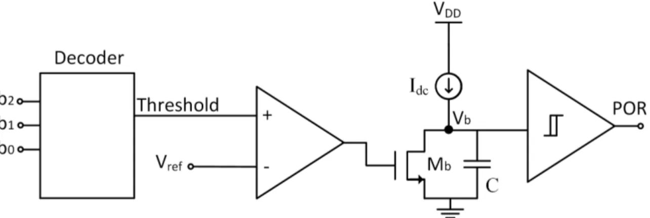
3.3 Top level decoder with 3 input bits. . . 36
3.4 Simplified schematic of the logic gates used in the decoder circuit. The PMOS and NMOS with undefined bulk have their bulk connected toVddand ground, respectively. . . 37
3.5 Decoder with 3 input bits. . . 37
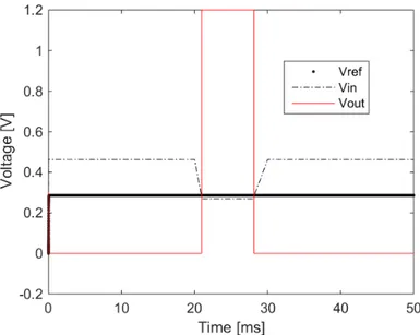
3.6 Resistive ladder. The NMOS with undefined bulk have their bulk grounded. 38 3.7 Comparator Output on the basis ofVin andVref. . . 40
3.8 Zoom of the Comparator Output on the basis ofVinandVref. . . 40
3.9 Simplified schematic of the comparator. PMOS and NMOS with undefined bulk have their bulk connected doVddand ground, respectively. . . 41
3.10 Comparator’s first stage output (Vo1) and last stage (Vout). . . 42
3.11 Simplified schematic of the Schmitt Trigger. PMOS and NMOS with undefined bulk have their bulk connected toVddand ground, respectively. . . 43
3.12 Variation in threshold output of the Schmitt Trigger with respect to the size of transistorsM1andM2. . . 44
L i s t o f Fi g u r e s
3.14 Variation in threshold output of the Schmitt Trigger with respect to the size of
transistorM5. . . 45
3.15 Variation in threshold output of the Schmitt Trigger with respect to the size of transistorsM6. . . 45
3.16 Monte Carlo simulations. . . 47
3.17 Power-On Reset & Brown-Out Reset simulations. . . 48
3.18 Power-On Reset & Brown-Out Reset simulations - zoom between 0 ms and 1.4 ms with aVdd rise time of 1 ms. . . 49
3.19 Layout implementation of the current source. . . 51
3.20 Current Source simulation results - schematic vs layout. . . 51
3.21 Layout implementation of the 3 bits decoder. . . 52
3.22 Layout implementation of the threshold. . . 52
3.23 Threshold simulation results - schematic vs layout. b) is a zoom of a). . . 53
3.24 Layout implementation of the comparator. . . 53
3.25 Comparator’s simulation results - schematic vs layout. b) is a zoom of a). . . 54
3.26 Layout implementation of the schmitt trigger. . . 55
3.27 Comparator’s simulation results - schematic vs layout. b) is a zoom of a). . . 55
3.28 Layout implementation of the POR-BOR. . . 56
3.29 POR-BOR’s simulation results - schematic vs layout. b) is a zoom of a). . . 57
4.1 Circuit implementation of proposed TIA. NMOS with undefined bulk have their bulk connected to ground. . . 60
4.2 Equivalent circuit model for the 65 nm RF NMOS transistor. . . 62
4.3 Small signal model of proposed circuit (complex model). . . 62
4.4 Small signal model of proposed circuit (simple model). . . 63
4.5 Comparison of simulated frequency response, a), and phase, b), of simple model, complex model and real model (Cadence). . . 65
4.6 Comparison zoom of simulated frequency response of simple model, complex model and real model (Cadence). . . 66
4.7 Comparison between the simulated frequency response of the simple model with all the parasitic capacitances and the simple model only with the Cgs capacitors. . . 68
4.8 Comparison between simulated frequency responses of diferent feedback re-sistance values. b) is a zoom of a). . . 70
4.9 Small signal model of proposed circuit (simplified model). . . 71
4.10 Input impedance calculation. . . 72
4.11 Transimpedance gain response of proposed TIA. . . 73
4.12 Simulated input referred noise. . . 74
4.13 Output eye diagram - a) without noise; b) with noise. . . 76
5.1 Current signal converted from the incoming optical signal by the PD. . . 79
5.2 AC decoupling circuit. . . 80
5.3 Block diagram of proposed circuit. . . 80
5.4 Circuit implementation of the proposed circuit. NMOS with undefined bulk have their bulk connected to the ground. . . 81
5.5 Simulations with and without offset cancellation block. b) is a zoom of a) and d) is a zoom of c). . . 82
5.6 Layout implementation of the offset cancellation. . . . 83
6.1 Biasing circuit. . . 86
B.1 Inverter schematic. PMOS and NMOS with undefined bulk have their bulk connected toVdd and ground, respectively. . . 99
B.2 Running a Layout File. . . 100
B.3 Layout File - GXL Editing. . . 100
B.4 Transistors of the inverter’s layout. . . 101
B.5 Choosing metal. . . 102
B.6 Drain connection with metal 1. . . 102
B.7 Gate connection with metal 1 and polly. . . 103
B.8 Bulks connected. . . 103
B.9 Bulks and sources connected. . . 104
B.10 Create a Pin. . . 104
B.11 Create a Pin. . . 105
B.12 Create a Label. . . 106
B.13 Final layout circuit. . . 106
B.14 Calibre DRC Config. . . 107
B.15 Example Calibre DRC. . . 107
B.16 Calibre LVS Config. . . 108
B.17 Example Calibre Correct LVS. . . 109
B.18 Example Calibre Incorrect LVS. . . 109
B.19 Calibre PEX Config. . . 110
B.20 Calibre View Setup options. . . 111
B.21 Example generated calibre view extracted schematic. . . 111
B.22 Schematic Simulation. . . 112
B.23 Schematic Output. . . 112
B.24 Environment Options. . . 113
L i s t o f Ta b l e s
2.1 Values of m for Shunt and Series Inductive Peaking . . . 23
2.2 Comparison of existing TIAs . . . 27
3.1 Decoder with 3 input bits Logic. . . 36
3.2 Left - Table of Truth NAND gate. Right - Table of Truth NOT gate. . . 37
3.3 Depending on the input bits, the reference voltage changes. . . 38
3.4 Transistor dimensions used in the comparator. . . 42
3.5 Monte Carlo simulations- Calculation of the offset. . . . 43
3.6 Monte Carlo simulations- Calculation of the gain. . . 43
3.7 Transistor dimensions used in the Schmitt Trigger. . . 46
3.8 Monte Carlo simulations- Calculation of the threshold when the capacitor is charging. . . 47
3.9 Monte Carlo simulations- Calculation of the threshold when the capacitor is discharging. . . 47
4.1 Static gain and bandwidth depending on the feedback resistance Rf, from Figure 4.8. . . 70
4.2 TIA simulation results - Gain. . . 75
4.3 TIA simulation results - Bandwidth. . . 75
4.4 TIA simulation results - Input reffered noise. . . . 75
4.5 TIA simulation results - Gain. . . 77
4.6 TIA simulation results - Bandwidth. . . 77
4.7 TIA simulation results - Input reffered noise. . . . 77
4.8 Comparison between the proposed TIA and the other existing TIA architec-tures. . . 78
5.1 Transistor dimensions used in the offset cancellation circuit. . . . 82
5.2 Resistances, capacitance and current values used in the offset cancellation circuit. . . 82
5.3 Simulation results without Offset Cancellation (OC). . . . 83
5.4 Simulation results with OC. . . 83
A c r o n y m s
Ad Open loop gain.
CERN Conseil Européen pour la Recherche Nucléaire.
CMOS Complementary metal-oxide-semiconductor.
DC-DC Direct current to direct current.
DRC Design Rule Check.
LA Limiting Amplifier.
LVS Layout vs. Schematic.
OC Offset Cancellation.
PD Photodiode.
PEX Practices Extraction.
PRBS Pseudorandom Binary Sequence.
SC Switched Capacitor.
SOC IC System on a Chip Integrated Circuit.
N o m e n c l a t u r e
Some of the most common and constant symbols used throughout the thesis are listed below.
Electrical Symbols
I Current
V Voltage
Units
A Ampere
dBm Decibel Miliwatt
dB Decibel
Hz Hertz
m Metro
rad Radian
s Second
V Volt
Mathematical Symbols
≈ Approximately equal to
loga(x) Base logarithmaofx
Other Symbols
f Frequency
C
h
a
p
t
e
r
1
I n t r o d u c t i o n
1.1 Context and Motivation
This chapter’s purpose is to contextualize the Transimpedance Amplifier sub-block and its function in an optical receiver to be implemented in a 65nm CMOS technology for a high-speed optical link (as well as other sub-blocks such as: a Power-on Reset and an Offset cancelling). It will be explained what motivated this project in the first place and
the main goals to be achieved during this work. It will also discuss some of the state of the art topologies and techniques for building and solving some of the most relevant problems associated with this type of amplifiers. Finally, a work plan will be presented as well as the chosen circuit topology and the respective theoretical analysis.
The European Organization for Nuclear Research, known as CERN ("Conseil Eu-ropéen pour la Recherche Nucléaire") performs high energy physics experiments at the LHC (Large Hadron Collider) so the need for a way to efficiently transfer the huge amount
of data originating from these experiments to the counting room is very pressing. Due to the radioactive character of these experiments the most practical way to do it is using optical fibre since it has a high tolerance to radiation and is almost immune to magnetic fields and electromagnetic noise.
It is therefore necessary to have a high speed radiation-tolerant optical receiver and the most economical way to do this is to have all the blocks embedded in the same IC (Integrated Circuit).
Figure 1.1: Optical Receiver Block Diagram.
1.2 Goal and Approach
In contrast to previous studies, the goal of this research is to go further and design a fully differential TIA compatible with a serial 5 Gb/s data rate. This requires enhanced
bandwidth and optimized transimpedance gain, input referred noise and group delay variation from the TIA.
To achieve wide bandwidth and low group delay variation, a differential TIA is
pro-posed. The Proposed design also combines regulated cascode and peaking inductors so as to have wide band response. Performance of the proposed TIA is compared with other existing TIAs, and the proposed TIA shows significant improvement in bandwidth and group delay variation compared to other existing TIA architectures.
1.3 Dissertation Structure
The following chapters of this document present the design of a trans-impedance ampli-fier for an optical receiver, starting from the state-of-the-art review through to the layout implementation and statement of the final conclusions. The chapters are structured as shown in the following summary:
• Chapter 1: Introductionpresents the work and proposes the implementation ap-proach. The motivations are outlined and the architecture is explained;
• Chapter 2: State of the Artshows the history behind the technology. Several inter-esting considerations are explored, in order to establish the background of existing TIA topologies. The search for new ideas and potential income;
• Chapter 3: Power-on Reset and Brown-Out Reset Implementation analyses and designs each sub-block making up the total block (POR-BOR);
1 . 3 . D I S S E R TAT I O N S T R U C T U R E
• Chapter 5: Offset Cancellation Implementationdiscusses the importance of can-celling the offset produced, for example, by device mismatch and drift due to
ther-mal variations. Lastly, the proposed OC circuit is presented.
C
h
a
p
t
e
r
2
S t a t e o f t h e A rt
2.1 Role and working principle of TIA
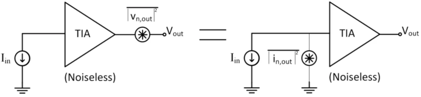
In an optical receiver, a transimpedance amplifier (TIA) is used to amplify a current signal,Iin, converted from the incoming optical signal by a photodiode (PD), to a voltage
signal, Vout [1]. The circuit is therefore characterized by several properties, including transimpedance gain, bandwidth and input referred noise current as shown in Figure 2.1:
Figure 2.1: Transimpedance Amplifier, Behzad Razavi-“Design of Integrated Circuits for Optical Communications".
The transimpedance gain of the TIA is the ratio of the output voltage to the input current.
|ZT(f)|=
Vout Iin
The noise contribution of the TIA is characterized by the input referred noise cur-rent. The input referred noise current is the noise current that could be applied to the equivalent noiseless TIA that would produce an output noise voltage equal to that in the original noisy circuit [1]. This is shown below in Figure 2.2.
Figure 2.2: Input Referred Noise Current, Behzad Razavi-“Design of Integrated Circuits for Optical Communications".
The input referred noise current is related to the output noise voltage by the following equation. I 2 n,in = V out 2 n,out Z 2 T (2.2)
The input referred noise current is used to provide a fair comparison between ampli-fiers since it does not depend on the transimpedance gain of the amplifier.
Equation 2.2 shows that it is necessary to calculate the noise at the output and then refer to the input, dividing the value calculated by the static gain.
To calculate the voltage noise in a transistor and resistance it is necessary to consider the resistance and transistor noises [1].
The thermal noise in a transistor can be represented by a current source connected between the drain and the source with a spectral power density given by,
I 2
n
≈4kT gm,
Figure 2.3a, where k is the Boltzmann constant and T is the temperature of the transistor. The thermal noise in a resistance can be represented by a current source in parallel with the resistor, where
I 2 n = 4kT
R , Figure 2.3b.
a Thermal noise in a transistor MOSFET. b Thermal noise in a resistance.
Figure 2.3: Thermal noise.
2 . 1 . R O L E A N D WO R K I N G P R I N C I P L E O F T I A
are independent, it is then possible to arrive at the sum of their contributions by adding up the power of each noise source (superposition theorem) as is shown in Figure 2.4.
Figure 2.4: Independent noise sources,"Design of Analog Cmos Integrated Circuits" [2].
2.1.1 Basic Transimpedance Amplifier
Since photodiodes generate a small current and most of the subsequent processing occurs in the voltage domain, the current must be converted to voltage [1]. As depicted in Figure 2.5, a resistor,RL, can perform this function, providing a transimpedance gain equal to −RLand leads to a severe trade-offbetween gain, noise and bandwidth.
Figure 2.5: (a) Conversion of photodiode current to voltage by a resistor, (b) equivalent cir-cuit for noise calculation, (c) effect of resistor value, Behzad Razavi-“Design of Integrated
Circuits for Optical Communications”. Used under fair use, 2013.
To calculate the noise voltage it is necessary to consider the noise from the resistance
RLand from the transistor. Knowing that the noise from the resistance is given byIn2=4RkTL
(noise current) and that the noise from the transistor is given byIn2= 4kT gm, the noise
voltage at the output can be obtained from,
V out2n,out= ∞ Z
0
ReplacingIn2= 4RkTL andRout=RL||sC1D in ( 2.3) results in the set of equations shown
below.
V outn,out2 = ∞ Z 0 4kT RL
RL|| 1
CDj2πf
df = ∞ Z 0 4kT RL
R2L
R2LCD24π2f2+ 1df
= kT
CD
(2.4)
Equation ( 2.4) shows that the total integrated noise is independent ofRL. However,
for a fair comparison it is more interesting to use the input referred noise, which can be obtained from the total integrated noise voltage ( 2.2):
I 2 n,in = V out 2 n,out Z 2 T = kT
R2LCD
(2.5)
Equation ( 2.5) indicates that, in order to reduce the input referred noise, the resistance value, RL, must be maximized. However, the 3-dB bandwidth (RB) of this particular
circuit, is given by the pole 2π R1
LCD. In short, the circuit’s properties are:
|ZT(f)|=RL (2.6)
I 2 n,in = kT
R2LCD (2.7)
RB= 1
2π RLCD
(2.8)
From equations ( 2.6) and ( 2.7) it is possible to conclude that in order to increase the gain and decrease the input noise, theRLresistance value should be increased. However,
when the resistance value increases, the bandwidth, in turn, decreases as is shown in equation ( 2.8). It therefore implies a trade-offbetween the gain, input noise, and
band-width that cannot be mitigated using a simple diode/resistor combination. Rather, it is important to create more complex structures that facilitate this trade-offand increase the
flexibility of design.
2.2 Common TIA topologies
2 . 2 . COM M O N T I A TO P O LO G I E S
the bandwidth requirements. It is also important to obtain high gain and low input noise, as low as possible. These two topics will be discussed later.
2.2.1 Open Loop TIAs
To obtain a low input impedance, open loop TIAs normally use a common base or a common gate topologies [1].
Figure 2.6: Common-gate.
Figure 2.6 shows a transistor M1 as a common-gate with a load resistor,RD (the gain
of this design is approximately equal toRD), and a transistor M2 operating as the bias
current source. To simplify the equations, the transistor M2 will be considered as the ideal current source.
Figure 2.7: Small-signal model of common-gate.
From Figure 2.7 it is possible to calculate the input impedance expression
Vin Iin
,Rin
[1], which results in:
Rin= rO+RD 1 + (gm+gmb)rO
If (gm+gmb)rO>>1 and, for long channel devices operating in the saturation region, rO>> RD is considered:
Rin≈
1
gm+gmb (2.10)
Equation ( 2.10) indicates that in order to reduce the input impedance, thegmand gmb must be maximized.
However, the downside of this common-gate is the input noise that the load resistor makes, caused by this circuit [1].
In,in2 =In,M2 2+In,RD2 (2.11)
SinceIn,M2 2= 4kT gm2andgm2=VGS22I−DV2T H2, whereID2andVGS2−VT H2are the drain
current and gate-source overdrive voltage ofM2, comes:
In,M2 2= 4kT 2ID2 VGS2−VT H2
(2.12)
In order to maintain the initial biasing conditions, operating saturation region in this case,RDID2must be less thanVDDandVDS2must exceedVGS2−VT H2 [1]:
4kT
In,RD2
+ 8kT
In,M2 2
< VDD ID2
(2.13)
Equation ( 2.13) shows that if load resistor increases, the input noise contribution ofRD decreases but, to maintain the initial biasing conditions, the bias current needs to
increase and therefore increases the input noise contribution ofM2. However, instead of
increasing the bias current, to maintain the transistor in saturation, the supply voltage may increase but the power consumption would also increase. In conclusion, this matter occurs because the input noise caused by the resistance load,RD, is directly proportional
to the bias current,ID2of the transistorM2.
2.2.2 Feedback TIAs
One of the most popular feedback TIAs is a shunt-shunt feedback structure. This is composed by a resistor,RF, which connects the output to theV−node, providing feedback
around an ideal voltage amplifier.
From Figure ( 2.8) andVX=−OpenloopgainVout (Ad) it follows that:
Vout Iin
=− Ad
Ad+ 1
RF
1 + RFCD Ad+1s
(2.14)
If considered an ideal amplifier, this will result in:
Vout
2 . 2 . COM M O N T I A TO P O LO G I E S
From equation ( 2.15) it is possible to conclude that increasing the resistance, RF,
increases the transimpedance gain.
Figure 2.8: Feedback TIA.
Returning to equation ( 2.14) (closer to the real), the bandwidth of this circuit is given by the following expression [1]:
f3dB≈
Ad+ 1 2π RFCD
(2.16)
From equation ( 2.16) it is possible to see the impact that RF has on f3dB. If the
resistance increases, the bandwidth will also decrease. Regarding to the input noise of this TIA, attention needs to be paid to the noise caused by the resistance, RF, and the
ampop [1].
Figure 2.9: Noises sources in feedback TIA.
For the sake of simplicity the input noise of the resistance will be considered, which results in [1]:
In,in2 ≈4kT RF
(2.17)
The noise fromRF is therefore directly applied to the input. This is similar to the load
resistor in the common-gate amplifier but the critical difference is that in the topology of
Figure 2.6, the resistance,RF, does not carry a bias current and therefore can be increased
2.3 Literature Review
2.3.1 Transimpedance Amplifier Topologies
2.3.1.1 Regulated Cascode TIA
As described in section 2.2.1, on the basic principles of a TIA open loop, a common-gate structure is usually used because it has a low input impedance. By having a low input impedance, the TIA will isolate the photodiode capacitance, preventing it from determining the bandwidth.
The ability of the common gate to isolate the large capacity of the photodiode is due to thegmof the input transistor. One of the solutions for decreasing the input impedance is
to increase the bias current and for this, the sizes of the transistors are increased. However, the downside of increasing the size of the transistors is that it also increases the size of the parasitic capacities on the transistor input. To solve this problem, a Regulated Cascode (RGC) TIA [3–7] has been used.
The schematic of the Regulated Cascode is shown in the figure 2.10. The current produced by the photodiode is converted to voltage through transistorM1and resistance
R1, from the pre-amplifier RGC. The resistanceRS is used to biasM1. The transistorMB
and the resistanceRBoperate as a local feedback to reduce the input impedance.
Figure 2.10: Regulated Cascode TIA.
With the body effect exclusion, caused by the transistorM1, the input impedance of
the RGC structure will be given by the following expression:
Rin≈
1
gm1(1 +gmbRB)
(2.18)
From equation 2.18 and comparing it with the input impedance equation of the common gate (excluding the body effect), 2.10 from section 2.2.1, it can be concluded
that the input impedance RGC structure is 1+g1
2 . 3 . L I T E R AT U R E R E V I E W
Due to this difference, it is possible to conclude that the RGC decouples the photodiode
capacitance better when determining the amplifier’s bandwidth.
This topology, RGC, was used in [3] to create a 1.25 Gbps TIA. The RGC was used as a current buffer followed by a voltage gain. This TIA was able to reach 58 dBΩwith a bandwidth of 950 MHz and a photodiode capacitance of 500 fF.
This topology was also used in [4] to create a 2.5 Gbps transimpedance amplifier. With a bandwidth of 2.2 GHz and a photodiode capacitance of 500 fF, the TIA is able to achieve 55.3 dBΩ.
[5] is another application of a topology RGC to create a 5 Gbps TIA. With a gain of 52.8 dBΩ, this RGC managed to achieve a bandwidth of 4.2 GHz with a photodiode capacitance of 1 pF.
The RGC was also used in [6] to create a 3.125 Gps TIA, which is very important in the optical communication subject. This TIA was able to achieve a gain of 72 dBΩwith a bandwidth of 2.4 GHz and a photodiode capacitance of 0.5 pF.
Lastly, the RGC structure was used in [6] to create a 4 Gbps single-to-differential TIA,
used as a current-amplifying. This TIA operates a bandwidth of 2.9 GHz, with a gain of 61.4 dBΩand a photodiode capacitance of 1 pF.
2.3.1.2 Feedback TIAs
This section describes a number of different feedback topologies. Figure 2.11 shows the
most common feedback structures.
Figure 2.11 a) shows a shunt-shunt feedback with a common source gain stage [8]. In order to convert the input current into voltage in the common source, a resistanceRD
needs to be connected to the drain node. To isolate the load resistance, RD, from the
feedback resistance,RFB, it is necessary to use a source follower.
Figure 2.11 b) describes the same topology but instead of using a common source gain stage, a cascode gain stage was used [9].
The common source gain stage is given by:
Vout
Iin =−gm(RL||rO) (2.19)
Thegmvariable is the transconductance of the transistor,RLis the load resistance and rOis the drain to source resistance of the transistor in saturation. IfrO>> RLthen:
Vout
Iin ≈ −gmRL (2.20)
The load resistanceRLis equal to the load resistanceRD (when transistorM2 is
ex-cluded), which is represented in Figure 2.11 a). It is concluded that the gain is directly proportional to the load resistanceRD. However, using a cascode structure,RL is given
by the common gate input impedance (excluding the transistorMband the body effect).
Rin≈
1
gm
(2.21)
From equation 2.21, since the Miller capacitance CGD1 (gate to drain capacitance
from transistorM1) can be calculated asC′=C(1−A), where A is the voltage gain, it is
possible to conclude that the Miller effect will decrease from:
C′≈C(1 +gm1RD) (2.22)
to:
C′≈C 1 +gm1
gm2 !
(2.23)
From equation 2.23, to simplify, it is consideredgm1=gm2which results in:
C′≈2C (2.24)
Returning to Figure 2.11 b), by placing a common gate (transistorM2) between the
transistor M1 (common source structure) and the load resistance RD, it is possible to
conclude from equation 2.24 that this will minimize the Miller effect.
Once the transistorM2 is in series with transistorM1 andRD, the current remains
the same, so the voltage gain is equal compared to the common source structure. The downside of the cascode structure is that it requires a higher supply voltage to maintain the same gain as the common source structure. The Miller Effect will be discussed in
detail in section 2.3.4.
(a) (b)
(c)
2 . 3 . L I T E R AT U R E R E V I E W
Figure 2.11 c) shows a CMOS inverter [10]. Using a PMOS transistor in this structure, it is possible to achieve a higher gain. One of the downsides of this topology is that it will increase the parasitic capacitance due to the use of PMOS transistors.
The common source topology was used in [8] to create a 2.5 Gbps optical receiver. This optical receiver uses a TIA with a shunt-shunt feedback structure. The TIA achieves a gain of 59 dBΩwith a bandwidth of 5.9 GHz.
The cascode topology was used in [9] to create a 5 Gbps optical receiver front end TIA. To minimize the Miller effect, this optical receiver also uses a TIA with a shunt-shunt
feedback and a cascode structure. As represented in Figure 2.11 b) [9], a source follower is used to isolate the load resistanceRD and feedback resistanceRFB. This TIA was able
to achieve a gain of 58.7 dBΩwith a bandwidth of 2.6 GHz and a photodiode capacitance of 200 fF.
The CMOS Inverter was used in [10] to create a 10 Gbps TIA using multiple inductive-series peaking. This technique will be discussed in detail in section 2.3.3.3.
2.3.2 Differential TIAs
Differential TIA, as shown in Figure 2.12, is usually employed to suppress supply voltage
and substrate noise. It also increases the output swing of a single ended structure to twice.
Figure 2.12: Pseudo-differential CG stage. [1]
There are three issues in this transimpedance almplifier that will be discussed [1].
Firstly, theVout1andVout2 output waves are asymmetric. This occurs because node
X will go through two different paths. On the one hand it operates as a common source
stage (transistorM3) in X-P path. On the other hand, it operates as a cascade of a source
Besides this, considering half of the circuit in Figure 2.12, the circuit’s input referred noise is√2 times the input referred noise of a single ended transimpedance [1].
Finally, even if the TIA differential circuit is perfectly symmetric, the output swings
are not fully differential. Figure 2.13 shows that when the diode, in Figure 2.12, is on,
Vout1andVout2 follow symmetric directions. However, if the diode turns off,Vout1and
Vout2become equal. This will make the threshold decision very difficult.
Figure 2.13: Output waveforms from a pseudo-differential CG stage. [1]
To avoid these issues, use of a fully differential TIA [11–14].
A fully differential topology was used in [11] to create a transimpedance amplifier for
an optical receiver based on wide-swing cascode topology. With a gain of 66 dBΩ, this TIA managed to achieve a bandwidth of 2.4 GHz with a 19.5 mW power consumption and 1.8 V voltage supply.
This topology was also used in [12] to create a transimpedance amplifier for an optical receiver. This TIA architecture shows a tunable transimpedance gain from 40 dBΩto 52 dBΩ, with a bandwidth of 5.6 GHz and 4.2 GHz, respectively.
In [13] a fully differential topology was also used. The TIA architecture, as shown in
Figure 2.14, is loaded by linear PMOS transistors in order to acquire the largest possible bandwidth. Once the cascade of stages gain increases much faster than the bandwidth decreases, there were used four cascade stages were used to have a higher gain and higher speed operation.
2 . 3 . L I T E R AT U R E R E V I E W
Cascading differential stages is also beneficial for the common-mode rejection of the
TIA [13]. This transimpedance amplifier managed to achieve a bandwidth of 2.9 GHz with a voltage gain of 73 dBΩ.
Last of all, a high-speed fully integrated optical receiver was used in [14]. The tran-simpedance amplifier structure achieved a voltage gain of 75.3 THzΩwith a bandwidth of 2.7 GHz and a photodiode capacitance of 1 pF. The current consumption of the full receiver was 187 mA for a supply voltage of 1.2 V [14].
2.3.3 Bandwidth Extension
The bandwidth of a gain stage is always limited by the capacitive load, usually at the output node that, along withRD, can result in a large time constant. However, sometimes the bandwidth requirements are not attainable. For that reason, it is recommended that bandwidth extension techniques be used.
This section will present some bandwidth extension techniques.
2.3.3.1 Capacitive Degeneration
Capacitive Degeneration is another bandwidth enhancement technique that consists in degenerating the transistors of a differential pair by placing a resistor and a capacitor
in parallel connected between the sources of the transistors, as shown in Figure 2.15. This effective ly increases the transconductance of the circuit at higher frequencies, which
compensates the voltage gain decrease due to the pole being at the output node.
Figure 2.15: Differential pair with capacitive degeneration [1].
Applying a single-ended analysis in this circuit (considering the half circuit) it is possible to calculate the transfer function for the equivalent transconductance,Gm, and
Gm(s) = gm(RsCss+ 1)
RsCss+ 1 +gmRs
2
(2.25)
From equation 2.25 it is possible to calculate the pole (equation 2.26) and zero (equation 2.27):
p=1 +gm
Rs
2
RsCs
(2.26)
z= 1
RsCs (2.27)
a b
Figure 2.16: Variation of the effective transconductance, Gm, and voltage gain with
fre-quency [1].
Figure 2.16 shows that the effective transconductance zero should be placed so as
to cancel the output node pole, thereby, extending the circuit’s bandwidth up to the transconductance pole. The disadvantage of this technique is that the voltage gain will decrease in order to keep the same GBW (relation between gain and bandwidth).
A capacitive source degeneration topology was used in [15] to create a 10 Gps tran-simpedance amplifier for an optical communication. With a gain of 51.7 dBΩ, this TIA was able to achieve a bandwidth of 8.5 GHz with an input referred noise of 4.9 pA/√Hz.
2.3.3.2 Shunt Peaking
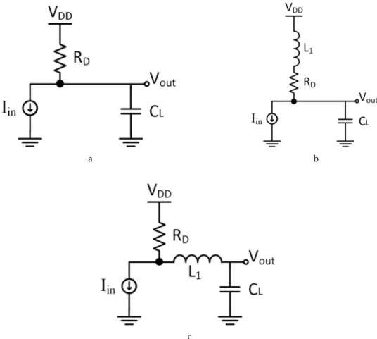
Shunt inductive peaking has been in use for a long time as a technique for extending circuit bandwidth. This method is called shunt inductive peaking because the resistor/in-ductor combination appears in parallel with the load capacitance. The key is to use an inductor in order to resonate the capacitance that limits the bandwidth.
Before looking at an example of a circuit that uses a Shunt inductive peaking tech-nique, it is important first to analyze a simple common source stage without a shunt peaking, as illustrated in Figure 2.17 a).
2 . 3 . L I T E R AT U R E R E V I E W
a b
c d
Figure 2.17: (a) Common source stage with load capacitance, (b) Small-signal equivalent of (a), (c) Common source stage with a Shunt Peaking, (d) Small-signal equivalent of (c) [1].
Vout Vin
=− gmRD 1 +CLRDs
(2.28)
p= 1
RDCL
rad/s (2.29)
From equation 2.29, assuming that this is the dominant pole in the system, the bandwidth of the amplifier is determined by theRDCLtime constant.
To improve the bandwidth, an inductorLPwas placed in series with the load resistance RD, as shown in Figure 2.17 c).
ApplyingVout
Vin in Figure 2.17 d), results in:
Vout Vin =−
gm(RD+LPs)
1 +CLRDs+CLLPs2
(2.30)
Frequency [Hz]
108 1010 1012 1014 1016
Common source Gain [dB]
-30 -25 -20 -15 -10 -5 0 5
w/o shunt peaking w/i shunt peaking
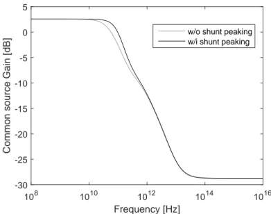
Figure 2.18: Bode Diagram of a CS amplifier with and without the shunt peaking tech-nique.
From Figure 2.18, it was concluded that including a shunt inductive peaking to cancel the load capacitance extends the bandwidth. Intuitively, when the frequency increases, the impedance looking into the load resistorRD increases and for that reason it will let more current flow to charge the capacitance.
The downside of using this technique is that adding an inductor will also add parasitic capacitances so that it is important to minimize the inductor’s size.
Many TIAs have been using this inductive peaking technique [16–18].
[16] describes a 10 Gps fully integrated optical receiver where shunt peaking is used. This circuit achieved 87 dBΩ with a bandwidth of 7.6 GHz. Operating under a 1.8 V supply, the power dissipation is 210 mW.
Shunt inductive peaking was also used in [17] to create a 2.5 Gps ultra-low-power TIA made in 90nm CMOS technology. This transimpedance amplifier operates a bandwidth of 2.68 GHz with a gain of 54 dBΩand total power consumption of 781.37µW.
Lastly, shunt inductive peaking technique was also used to create a transimpedance amplifier for 10 Gbps optical application [18]. The TIA consumed 18 mW to achieve a voltage gain of 59 dBΩ with a bandwidth of 8.6 GHz in the presence of a 0.15 pF photodiode capacitance from a 1.8 V supply.
2.3.3.3 Series Inductive Peaking
Section 2.3.3.2 looked at the shunt peaking technique. However, it is also possible to use inductive peaking in series with load capacitance.
Another bandwidth extension technique is the Series Inductive Peaking. Unlike the Shunt peaking, this technique involves placing an inductorLP in series with the load
2 . 3 . L I T E R AT U R E R E V I E W
inscreasing the bandwith and, consequently, improving the speed.
The load capacitance receives more current because when the frequency increases near the resonance frequency, the impedance looking into the load capacitance will be reduced, as shown in equation 2.31.
Zequivalent=s LP//(s CL)−1
= s LP
s2LPCL+ 1
(2.31)
In order to maximize the flat frequency response or group delay, the inductorLP can
be adjusted. A more detailed analysis to adjust the inductor in shunt peaking and series inductive peaking techniques will be discussed in section 2.3.3.4.
Series inductive peaking has been used, as mentioned in section 2.3.1.2, to create a 10 Gps transimpedance amplifier in 0.18µm CMOS technology in [10]. As shown is Figure 2.19, a TIA is used as a multi-stage amplifier with a series inductive peaking technique in each stage, in order to increase the bandwidth and therefore the circuit speed.
Figure 2.19: Transimpedance amplifier using series inductive peaking.
Usually, when a cascade topology with PMOS transistor is used, the bandwidth is fre-quently degraded because of the large parasitic capacitances added by PMOS transistor.
Another reason to reduce the bandwidth is because the series inductive peaking is not used in circuits. Thus, the usage of inductors, as shown in Figure 2.19, makes possible to absorb the parasitic capacitance’s effect and therefore the bandwidth increase.
It was performed a simulation in [10] in order to conclude that the usage of a five stage amplifier makes possible to increase the bandwidth up to three times when using the series inductive peaking technique.
The transimpedance amplifier in [10] achieved a gain of 61 dBΩwith a bandwidth of 7.2 GHz.
2.3.3.4 Shunt vs Series Peaking
to make a comparison between these two implementations in three characteristics:
• Maximum Bandwidth;
• Maximally Flat Frequency Response;
• Maximally Flat Group Delay;
In order to compare the above characteristics, the three circuits, shown in Figure 2.20, will be analyzed.
a b
c
Figure 2.20: Various Methods of Inductive Peaking a) RC Circuit Without Inductive Peaking b) Shunt Inductive Peaking c) Series Inductive Peaking.
Figure 2.20 a) shows a circuit implemented by placing a load resistanceRD in parallel
with a load capacitanceCL. The load resistanceRD is used to create a pole with the load capacity. Assuming that it is the dominant pole, the bandwidth is determined by the time constant (RDCL)−1.
In order to increase the bandwidth it is possible to decrease the resistanceRD.
How-ever, this will increase the input noise, as already mentioned in section 2.1.1.
2 . 3 . L I T E R AT U R E R E V I E W
The difference between the Figure 2.20 a) and Figure 2.20 b) is that the latter an
inductorL1in series with the load resistanceRD. This technique, as mentioned earlier, is
known as shunt peaking because the inductor is in parallel with the load capacitance. Finally, the difference between the Figure 2.20 a) and Figure 2.20 c) is that the latter
an inductorL1in series with the load capacitanceCLto generate the resonant circuit. This
technique, also mentioned earlier, is known as series inductive peaking.
Based on the techniques previously studied, it is possible to conclude that even if the size of the inductor is increased, the circuit’s bandwidth will always reach a point where bandwidth growth is saturated and it will also cause an unwanted peak not only in frequency response but also in group delay.
Consequently, in [19], it is possible to calculate the value of the inductorL1in order
to maximize the flat frequency response, maximize the flat group delay or maximize the bandwidth. The inductorL1is calculated as follows:
L1=m R2DCL (2.32)
Where m is a numerical value that determines the type of response from the circuit and its value is given in Table 2.1 [19].
Table 2.1: Values of m for Shunt and Series Inductive Peaking
Response Shunt Inductive Peaking Series Inductive Peaking
Maximally Flat Frequency Response 0.4 0.5
Maximally Flat Group Delay 0.3 0.333
Maximum Bandwidth 0.76 0.53
In order to compare the bandwidth increase, using inductive shunt peaking and series inductive peaking, it is possible to observe the frequency response and step response presented in Figure 2.21 for each type of peaking.
Figures 2.21 a) and b) show the frequency response and step response that maximize the flat frequency response of each circuit. It is possible to conclude that the shunt inductive peaking technique increased 1.73 times more bandwidth than the unmodified RC circuit. It should also be noted that the series inductive peaking technique increased 1.42 more bandwidth than the unmodified RC circuit.
Figures 2.21 c) and d) show the frequency response and step response that maximize the flat group delay of each circuit. With the maximization of the flat group delay it is possible to conclude that the shunt inductive peaking technique had an enhancement of 1.58 compared to the unmodified RC circuit. On the other hand, the series inductive peaking technique increased 1.39 more bandwidth than the original circuit. It should also be noted that, in this circuit, both the techniques used to increase the bandwidth ran out of overshoot, i.e. managed to reach the desired value more quickly.
However, the series inductive peaking technique has not improved much compared to the results obtained in the flat frequency response study. The downside of maximizing the bandwidth is that an unwanted peak appears near to the frequency response and therefore an overshoot in step response, when using these techniques (shunt and series inductive peaking).
a b
c d
e f
2 . 3 . L I T E R AT U R E R E V I E W
2.3.4 Miller Effect
As mentioned in section 2.3.1.2, the Miller effect is a very important concept that needs
to be understood, together with the solutions for decreasing it.
From Figure 2.22 it is possible to conclude that there is an overlap between the gate and the drain which creates parasitic capacitances between them. In short gate length devices, this overlap capacitance is significant compared to other parasitic capacitances and so it is fundamental to consider that.
Figure 2.22: Transistor structure.
In a common source circuit, Miller’s capacitance is the name given to the parasitic ca-pacitance between the gate and the drain,CGD,because it is the capacitance that connects the input to the output, as shown in Figure 2.23.
Figure 2.23: Transistor structure.
Miller’s theorem, in [20], says that it is possible to replace the CGD by two shunt
capacitances in the input and output, as shown in Figure 2.24.
Figure 2.24 shows that a series admittance is connected between two points with a known voltage gain of K.
In order to replace the admittance by two shunt admittances in input and output, it is necessary to consider two currents,I1andI2, that remain the same throughout the whole
Figure 2.24: Miller Theorem.
First of all it is important to know the equations capable of determining the currents
I1andI2, as shown on the left side of the Figure 2.24:
I1= (V1−V1K)Y (2.33)
I2= (V1K−V1)Y (2.34)
Emphasising V1, results in:
I1=V1(1−K)Y (2.35)
I2=V1(K−1)Y (2.36)
So it is possible to equate 2.35 and 2.36 to the currents, as shown at the right side of the Figure 2.24:
V1(1−K)Y =V1Y1 (2.37)
V1(K−1)Y =K V1Y2 (2.38)
The shunt admittances’ values can be determined by the following expressions:
Y1=Y(1−K) (2.39)
Y2=Y(1−
1
K) (2.40)
From Equations 2.39 and 2.40, it is concluded that, with an increase in the circuit’s
K gain, the input impedance will also increase and, in turn, the frequency of the pole will decrease. The bandwidth will therefore decrease. However, as mentioned in section 2.3.1.2, there are techniques capable of decreasing the Miller effect.
2.3.5 Comparison of published TIAs
2 . 3 . L I T E R AT U R E R E V I E W
Table 2.2: Comparison of existing TIAs
Reference Process Bit Rate (Gb/s) ZT (dBΩ) BW (GHz) Spot noise (pA/√Hz)
[4] 0.6µm 2.5 55.3 2.2
-[6] 0.18µm 3.125 72 2.4
-[7] 0.18µm 4 61.4 2.9 26.8
[9] 0.18µm 5 58.7 2.6 13
[10] 0.18µm 10 61 7.2 8.2
[11] 0.18µm 2.4 82 2.4 36
[13] 0.13µm 4.5 73 2.9
-[15] 0.18µm 10 51.7 8.5 10
[16] 0.18µm 10 87 7.6
-[17] 90 nm 2.5 54 2.68 4.9
[18] 0.18µm 10 59 8.6 25
2.3.6 Power-on Reset and Brown-Out Reset
Power-on-reset (POR) circuits are an essential component of the System on a Chip Inte-grated Circuit (SOC IC).
The primary function of a POR circuit is to control and initialize critical nodes in analogue and digital circuits. The circuit should issue a reset signal keeping the system in the reset state until the power supply reaches a steady-state level (or at least a level at which the circuits are able to operate).
This signal is then used to initialize various nodes in analog and digital circuitry surrounding the POR circuit.
The POR signal stays at logic 1 (Reset) as long as the power supply is below a certain voltage, also called Brown-Out (BO) voltage [21]. When BO reaches the supply voltage or a certain voltage that makes the circuit work properly, the POR output is changed to logical level 0.
During normal operation, sudden disturbances in the power supply line (heavy cur-rent drawn by the load) can also lead the circuit to malfunction (brown-out event). In order to ensure proper operation after the brown-out event, the reset signal should be generated to bring all circuits to a well defined state. The circuit responsible for monitor-ing power supply line and generatmonitor-ing reset signal is known as Brown-Out Reset (BOR) circuit.
Figure 2.25 shows the time relation between the POR & BOR and the supply voltage,
Vdd.
Figure 2.25: POR and BOR methodology.
2.4 Radiation E
ff
ects on CMOS Technology
In order to use microelectronics in high-energy physics experiments they need to be hardened against the radioactive environment in which they are placed. It is therefore of the greatest importance to study the radiation effects in modern CMOS process.
These effects are known as Total-Ionizing Dose (TID) Effects and are caused by
con-tinuous exposure to radiation and are characterized by permanent changes in electronic devices.
2.4.1 TID Effects on Modern CMOS Process
TID radiation effects on CMOS devices are mainly related to the charging in the
ox-ides and the consequent effects of this charging. These phenomena have a large impact,
especially, in the gate oxides (possibly causing deterioration of some of the transistor per-formance parameters), in the transistor edges (possibly causing leakage current between the adjacent transistors) and in the isolation oxides (possibly resulting in an inter-device isolation loss) [22].
2.4.1.1 Gate Oxide Effects
The ionizing radiation effects rely on electron-hole pairs formed in the oxide. When a
high-energy particle impacts a solid, it ionizes the lattice atoms forming these pairs at a constant rate, while the particle loses energy as it passes through it. Part of the pairs recombine themselves in the gate oxide while the remaining electrons and holes take opposite directions in the applied electric field [22].
Electrons move towards the gate. Due to their high mobility in the SiO2 the gate
contact is quickly outpaced and no electrons remain in the gate oxide. On the other hand, holes are trapped in the oxide gate (they have low effective mobility), creating a net
2 . 4 . R A D I AT I O N E F F E C T S O N CM O S T E C H N O LO G Y
Figure 2.26: Charge distribution in a gate oxide at three times after exposure to a pulse of irradiation at t = 0 for a thick gate oxide. (a) t = 0−, (b) t = 0+, (c) t = 0++ , and (d) t>>0++ [22].
While the oxide trapped charge is always positive, the interface trapped charge state depends on the bias conditions and the device type. The interface states act as negative charges in the gate-oxide of a NMOS transistor, or positive charges in the gate-oxide of a PMOS transistor [22].
The introduction of these new charge sources can affect the device’s performance. The
trapped charge in the gate oxide and/or at theSi/SiO2 interface induces a shift in the
CMOS transistor threshold voltage∆VT.
2.4.1.2 Radiation-Induced Leakage Current
Previously introduced in section 2.4.1.1, electron-hole pairs are created along the track of the impinging particle. The positive charge trapped in the field oxide due to ionizing radiation, in a NMOS device, can invert the underlying P-doped region and form a con-ducting channel between the source and drain terminals as depicted in Figure 2.27 a) [22].
This process results in two conductive paths as shown in Figure 2.27 b), resembling parasitic transistors in parallel with the main device. This also results in a shift in the effective threshold voltage, sometimes large enough to create a source-drain current in
the transistor at offstate (VGS = 0) as shown is Figure 2.28.
Figure 2.27: a) Radiation-induced hole trapping in thick isolation field oxides driving the parasitic field oxide transistor into inversion. b) Parasitic conductive paths [23].
Figure 2.28: Increase of the sub-threshold current in an n-channel transistor given by a decrease in the threshold voltage [24].
2.4.1.3 Hardness-by-Design Techniques
Hardness-by-design is a method for designing radiation-tolerant microelectronic com-ponents without the use of special manufacturing processing techniques (hardening-by-process). In this section, some design techniques used to mitigate TID effects will be
addressed.
In order to eliminate radiation-induced edge leakage, introduced in section 2.4.1.2 and based on conductive parasitic paths between a device source/drain, an enclosed layout can be used, as shown in Figure 2.29, and hence, there will be no edge leakage. [22].
Other technique is the usage of a p+ diffusion ring preventing the inversion of the
p-substrate at the interface between the field oxide, as shown in Figure 2.30.
2 . 4 . R A D I AT I O N E F F E C T S O N CM O S T E C H N O LO G Y
Figure 2.29: CMOS transistor with an enclosed layout [23].
Figure 2.30: Cross-section of a CMOS process with a p+ channel stop designed into the FOX isolation [22].
C
h
a
p
t
e
r
3
P r o p o s e d P O R- B O R C i r c u i t
As previously discussed in section 2.3.6 of chapter 2, one of the parts of this project is to design a circuit that produces a reset signal when the supply voltage falls below a reference voltage.
It starts with the description of the block and in general was conceived and designed to meet all of CERN’s requirement, i.e. that it should:
• Work for wide temperature range (from -20 to 100 ºC) and all process corners;
• Be low power (< < 1mW after reset is released);
• Provide 3 active high reset signals for redundancy due to radiation effects (Triple
modular Redundancy used in lpGBTX);
• Ensure a proper reset of the chip for supply voltage rise times from 1µs to 10ms;
• Have an external reset pin;
• Have a brownout detection circuit configured with different reference voltages, e.g.
0.7V to 1.05V;
• Be designed in TSMC 65nm 6M technology;
A detailed explanation is also provided of the function of each sub-block (originating the POR) and why they were used.
3.1 Proposed Circuit
As mentioned above, in line with CERN’s requirements, a circuit that performs the in-tended function has been designed.
Figure 3.1: Top level schematic POR-BOR. The NMOS with undefined bulk have their bulk connected to ground.
Figure 3.1 shows the simplified schematic of the proposed Power-on Reset and Brown-Out Reset.
It is important to understand the general functioning of the circuit. When a power supply is switched on, the supply voltage gradually rises and the current generator re-mains off. So the capacitor voltageVbis low. During this period, the output of the Schmitt
Trigger (POR) tracks the supply voltageVdd. When theVddexceeds the threshold voltage
of the current generator, the current generatorIdcstarts to charge capacitance C. When Vb exceeds the high switching point of the Schmitt Trigger, the POR signal goes lower
and so the reset phase is over.
The duration of the reset signal is set by the currentIdc, the capacitance C and the the
high switching point of the Schmitt Trigger.
If the supply voltage drops, the current generatorIdc switches offand theVbis very
slowly discharged (only by leakage currents). In order to speed up the circuit response to brown-out events, a brown-out detector is added. It compares the supply voltage with a voltage reference and if the supply voltage is too low, the transistorMbis opened, shorting
the capacitor C.
Once the capacitance voltageVbdrops below the low switching point of the Schmitt Trigger, the Schmitt Trigger turns one and generates the reset pulse. When the supply volt-age is high enough, the transistorMbis opened, the process of charging the capacitance
C starts and the circuit behaves as during the power-on process.
3.1.1 Current Source
3 . 1 . P R O P O S E D C I R C U I T
Figure 3.2: Current source with Schmitt Trigger. The PMOS with undefined bulk have their bulk connected toVdd.
In order to obtain an acceptable capacitor charging time (between 10µs to 30µs with a capacitor value of 4pF) and to reduce the power of the circuit, a current source of 200nA has been used, because:
Vb= T
Z
0
ic(t)
C dt (V)
= I
Ct (V)
(3.1)
ReplacingI = 200nA,C= 400pFin ( 3.1) andVb= 0.95 results in:
0.95 = 200 10−
9
4 10−12 t (V)
t= 18 (µs)
(3.2)
From equation ( 3.2) it was concluded that the 4pF capacitance needs only 18µs to reach 0.95V.
Once this block (POR-BOR) works in a time interval between 1µs to 10ms, the 18µs becomes an acceptable result for the capacitor’s charging time.
3.1.2 Decoder with 3 bits and Threshold Voltage
CERN has requested a block that would be able to generate multiple reference voltages from the power supplyVdd with 3 input bits.
Figure 3.3: Top level decoder with 3 input bits.
Table 3.1: Decoder with 3 input bits Logic.
S3 S2 S1 D1 0 0 0
D2 0 0 1
D3 0 1 0
D4 0 1 1
D5 1 0 0
D6 1 0 1
D7 1 1 0
D8 1 1 1
To design the decoder and following the logic as shown in table 3.1, some background knowledge of logic is required.
3.1.2.1 Logic Gates
Logic gates or logical circuits are devices that operate one or more logical input signals to produce an output signal. In the output there are 2 possible outcomes:
• Signal presence or "1" (true);
• Absence of signal or "0" (false);
The decoder, is implemented by using combinations of NAND and NOT gates. Figures 3.4 show the simplified schematic of these gates. All the logic gates are designed with the minimum length (L) and width (W) allowed by the technology, in order to reduce the area and power dissipation.
Figures 3.4 a) and b) show the table of truth by using a NAND and a NOT gates, respectively.
With this information it is now possible to implement a decoder by using NAND and NOT gates as shown in Figure 3.5.
From Figure 3.5 it is possible to enable 8 different reference voltages due to the 8
![Figure 2.16: Variation of the e ff ective transconductance, Gm, and voltage gain with fre- fre-quency [1].](https://thumb-eu.123doks.com/thumbv2/123dok_br/16581985.738578/42.892.146.763.292.631/figure-variation-ective-transconductance-gm-voltage-gain-quency.webp)
![Figure 2.28: Increase of the sub-threshold current in an n-channel transistor given by a decrease in the threshold voltage [24].](https://thumb-eu.123doks.com/thumbv2/123dok_br/16581985.738578/54.892.273.631.492.758/figure-increase-threshold-current-channel-transistor-decrease-threshold.webp)