Cheng Yuhua, Wu Xiaobo, Yan Xiaolang
Abstract—A hybrid translinear (TL) circuit constituted by two kinds of transistors, bipolar and CMOS transistors, was proposed to control its quiescent current. And a new method was introduced to analyze the hybrid TL circuit, which converted it into an uniform equivalent bipolar TL circuit. It simplified its analysis and design. This hybrid TL circuit is applied to the output stage of a class AB amplifier. The simulation results in 1.5μm BCD (Bipolar-CMOS-DMOS) technology were consistent with expectations well.
Index Terms—translinear circuit, hybrid integrated circuit, differential pair, quiescent current control
I. INTRODUCTION
The translinear principle proposed by Gilbert in 1975 is one of the important contributions to circuit theory in the electronics era [1]. Generalized translinear principle which applies to devices having transconductance linear with an electrical variable such as current or voltage has been proposed by [2]. In this paper the hybrid translinear circuit containing both bipolar and CMOS transistors was proposed and analyzed. And its application to the output structure of the class AB amplifier to control the quiescent current was given, which offered three types of output structure for comparison. All circuits were simulated in 1.5μm BCD (Bipolar-CMOS-DMOS) technology and the results are consistent with expectations well.
II. HYBRID TRANSLINEAR CIRCUIT
If the transconductance is linear with current, thus /
g=dI dV =aI (1)
exp( ).
I =b aV (2)
This work is sponsored by the National Natural Science Foundation of China under grant No.50237030 and 90207001. It also gains support from the National Semiconductor Corp. (NSC).
Cheng Yuhua is with the Institute of VLSI Design, Zhejiang University Hangzhou, 310027, China, (phone: +86 571 87952662; fax: +86 571 87952486; e-mail: [email protected])
Wu Xiaobo is with the Institute of VLSI Design, Zhejiang University Hangzhou, 310027, China, (e-mail: [email protected])
Yan Xiaolang is with the Institute of VLSI Design, Zhejiang University Hangzhou, 310027, China, (e-mail: [email protected])
This is an exponential current-voltage characteristic of bipolar transistor or MOS transistor working in weak inversion.
If the transconductance is linear with voltage, it can be expressed as
/
g=dI dV =aV (3)
2
/ 2 .
I=AV +B (4)
This is a square law current-voltage characteristic of MOS transistor working in strong inversion.
Although BTL (Bipolar TL) circuits are better in matching than MTL (MOS TL) ones due to their process, the advantage of MTL is that it can be easily adjusted by the aspect ratios of MOS transistors to achieve high accuracy, which is more convenient than BTL that is adjusted by the areas. Besides, the zero DC gate current of MOS transistor and low power dissipation are also its advantages. For MTL and BTL work in different manners, they have different appropriate applications. It was introduced in many papers.
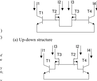
It should be pointed out that in some situations it is difficult to satisfy the requirements by using onefold bipolar or CMOS transistor. So a hybrid TL circuit that consists of both CMOS and bipolar transistors is needed. Fig. 1 shows the basic structure of a hybrid translinear circuit which has two structures similar to MTL or BTL circuit respectively. One is up-down structure and the other is stacked structure. They fit the same equation according to kirchhoff’s voltage law. That is
T1 T2 T3 T4
I1 I2 I3 I4
(a) Up-down structure
T1
T3 T2
T4 I3
I1 I4
I2
(b) Stacked structure
(a)
(b) Fig. 2. A model of HTL
1 3 4
be gs be gs
V +V =V +V 2
3
2
.
(5)
1 4 2 .
be be gs gs
V −V =V −V (6)
Changing from (5) to (6) will bring the benefit later. A model to analyze the HTL circuit will be proposed in section III.
III. AMODEL OF TLCIRCUIT
The TL loop shown in Fig. 1 can be divided into two differential pairs because the currents of I1 plus I4 and I2 plus I3 are always kept constant (i.e. the tail current is kept constant ideally). So the hybrid TL is divided into two differential pairs which are shown in Fig. 2. Similarly, the stacked structure can also be divided as shown in Fig. 2 since the input signals of the sources of T2 and T3 are equivalent to that of the gates of T2 and T3. Both they change the Vgs but in different ways.
From Fig. 2(a) it can be seen that 2
1 2 3
2Itail /
β
=(Vgs −VTH) +(Vgs −VTH) (7)Bipolar differential pair working in weak inversion is similar to the MOS one. From Fig. 2(b) it can be derived:
1 0 4 0
2
exp(
be) exp(
be).
T T
V
V
V
V
V
V
−
−
=
+
(8)Here V0=VTln(Itail2/2).
The graphic models of a MOS differential pair in strong and weak inversion were proposed respectively [3]. That of the bipolar differential pair is similar to the weak inversion one. Fig. 3 shows the graph model of MOS differential pair in strong inversion and that of bipolar one respectively.
Although two curves are different due to their different laws,
(a) The effective gate-source voltage Vx (Vx=Vgs2–VTH) versus Vy (Vy=Vgs3–VTH) and the differential input voltage Vin
(b) The effective base-emitter voltage Vx (Vx=Vbe1–V0) versus
Vy (Vy=Vbe4–V0) and the differential input voltage Vin. Fig. 3. The graphic model of Fig. 2
their trends are alike. If Vin is reflected in the new coordinate, the difference will be smaller. From (6) it is known that the equal Vin is the essential requirement and the two differential pairs can be replaced by each other while considering the voltage relationship. So MTL, BTL and HTL circuit could be uniform.
IV. APPLICATION IN CLASS ABOUTPUT
(a) CMOS output structure
(b) I2 versus I1
Fig. 4. CMOS output stage
controlled lower, more convenient and more accurate by adjusting the W/L. And the quiescent current control component uses bipolar to get better matching.
If Iref=I9=I10=1/4Itail, β1-β13 are equal and β1=β2, with the MTL loops M1, M11, M14, M12 and M1, M11, M13, M9 in Fig. 4(a),
2 2
1 2
11 1 11 2 11
( ) ( )
2
tail tail tail
I I I I
.
I
β
−β
+β
−β
=β
. ef
(9)
The quiescent current is
1 / 13
q ref r
I =
β
Iβ
=MI (10)And the residual output current while the other output transistor is heavily driven is found from (9):
2
1 2
( )
2
residual tial
I = − MI . (11)
M is the ratio of W/L of transistors M1 and M14, M2 and M6. The output structure composed by fully bipolar transistors is shown in Fig. 5(a).
The BTL loops Q1, Q11, Q14, Q12 and Q1, Q11, Q13, Q9 are similar to the MTL loops in Fig. 5(a). It can be derived that
1 2/( 1 2) ref/ 2.
I I I +I =MI (12)
(a) Bipolar output structure
(b) I2 versus I1
Fig. 5. Bipolar output stage
It is a harmonic-mean value. The quiescent current and residual current are
q
I =MIref (13)
. 2
residual ref
M
I = I (14)
The mixed output structure constituted by both bipolar and CMOS transistors is shown in Fig. 6(a).
With the HTL loops M1, Q11, M14, Q12 and M1, Q11, M13, Q9, it can be derived that
1 2
13
1 2
2
2 2
1/ exp( ) 1/ exp( ) 2 / exp( ). ref
T T
I
I I
V V
β
β β
+ =
T V
ref
(15)
The quiescent current and residual current are
q
I =MI (16)
2 1( 2 / 13 ln 2) / 2
residual ref T
I =
β
Iβ
−V (17)It can be seen that the quiescent currents in three cases are all equal, and their residual currents are not too small to cut off the output transistor while other transistors are under heavy driving. They are determined by equation (9), (12), (15).
(a) BiCMOS output structure
(b) I2 versus I1
Fig. 6. BiCMOS output stage
2
1 2
(2− I ) +(2− I )2=2 (18)
1 2
1/I +1/I =2 (19)
1 2
1 1
exp( I ) exp( I ) 2.
λ
λ
− −
+ = (20)
Here, λ= 2β1VT.
The minimum current of (18) is 0.34 times of quiescent current that accords to the depiction in [4].
And the minimum current of (19) is 0.5Iq. But the minimum current of (20) is not a certain value. It is about 0 - Iq.
The graphs of the three equations are depicted in Fig. 4(b), Fig. 5(b) and Fig. 6(b) respectively. All of them can reach quiescent current control. It approves the uniformity of MTL, BTL and HTL circuit. Moreover, it can be seen that the three curves have different ascending curvature and the exponential ones are steeper than the square law one. That means if BTL or HTL circuits with exponential curves are applied to current control, the more accurate quiescent current control is available. On the other hand, since MOS transistors have zero dc gate-source currents, the output circuits consisting of MOS devices have higher accuracy than bipolar ones. But bipolar circuits are better for matching and getting lower offset that is of importance to the fractional change in the quiescent current of the error amplifier [6].
As results, HTL circuit is the best choice for accurate and convenient quiescent current control.
(a) I1 and I2 versus Vcm
(b) I2 versus I1
Fig. 7 Simulation result of Fig. 6
Fig. 8. Layout of the amplifier Output stage
V. SIMULATION RESULT
VI. CONCLUSION
In this paper, a hybrid TL circuit (HTL circuit) and a new method for TL circuit analyzing were proposed, which divides the HTL circuit into two differential pairs and converts them into an equivalent bipolar TL one to simplify its analysis and design. As example, three types of TL circuit were successfully uniformed. And an application of HTL circuit to the output stage of a class AB amplifier was developed. In comparison with onefold MTL or BTL circuit, it could get lower quiescent current variation and more accurate quiescent current control. The simulation results were given and it is proved that the results are consistent with the theoretical results accurately.
ACKNOWLEDGMENT
The author would like to thank Mr. David Pace and Mr. Kalon Chu, the senior engineers of NSC, for their useful discussion and instruction.
REFERENCES
[1] B. Gilbert, “Translinear circuits: A Proposed Classification,” Electron. Lett., vol. 11, no. 1, pp. 14–16, 1975.
[2] Evert Seevinck and Remco J. Wiegerink, “Generalized Translinear Circuit Principle,” IEEE J. Solid-State Circuits, vol. 26, no. 8, August 1991.
[3] Nabil I. Khachab, Peter A. Wassenaar, and Roelof F. Wassenaar “A Graphical Model of a MOS Differential Pair in Strong and Weak Inversion,” Microelectronics, The 14th International Conference on 2002 – ICM.
[4] Op't Eynde, F.N.L., Ampe, P.F.M., Verdeyen, L., and Sansen, W.M.C., “A CMOS Large-swing Low-distortion Three-stage Class AB Power Amplifier,” IEEE J. Solid-State Circuits, vol. 25, no. 1, february 1990. [5] Alan Hastings, The Art of Analog Layout. Pearson Education, inc. 2004,
pp. 104.
[6] Paul R. Gray, Paul J. Hurst, Stephen H. Lewis and Robert G. Meyer,