Cornel HaŃiegan
We investigate the semiconductor heterostructure with the Ben Daniel Duke model applied for the lowest conduction states Ga As Ga (1) as and for the heavy levels at
k
⊥=
0
in any heterostructures (1). In a quantic level we obtained the familiar staircase density of states (2). In (3) we calculated the incrgy position of the interface state in a single HgTe CdTe heterojonction. We also obtained the existence of the inter face state relies only on the relative position of the I’8 edges of HgTeand CdTe, their actual energy position, as well as their behavior at
0
≠
⊥
k
.Ben Daniel Duke model, heterostructure, quantum well, Ben Daniel Duke quantum well
Equation(19) defines the in plane effective mass of the
n
th sub band in the vicinity ofk
⊥=0. It may be remarked that ifm
B>
m
A, as is the case in GaAs Ga(Al)As orGa
0.47In
0.53As
−
InP
,this in plane massm
n will increase with increasing sub band index nUsing the approximately parabolic in plane dispersion laws (equation (14)) it is very easy to calculate the density of states p
(
ε
)
associated with the bound statesE
n. Proceeding exactly as in chapter I we obtain:∑
=
n n
p
p
(
ε
)
(
ε
)
(20a))
(
)
(
n2 nn
Y
E
h
S
m
p
=
ε
−
π
ε
(20b)where Y(x) is the step function. We recover the familiar staircase density of states. The properties of a Ben Daniel Duke quantum well are summarized in figure 4.
ANALELE UNIVERSITĂłII
“EFTIMIE MURGU” RE IłA
From the left to the right: conduction band edge profile, energy levels
2 1
andE
E
and their associated envelope functions; in plane dispersions of theE
1and
E
2 sub bands; energy dependence of the heterostructure density of states).
(
ε
p
! "# A recollection of the main properties of the quantum well bound states, solutions of a Ben Daniel Duke Hamiltonian.
$#% & & '
(
m
Am
B<
0
;
k
⊥=
0
)The case
m
Am
B<
0
is practically realized in HgTe CdTe heterostructures [20] (see Fig. 5). CdTe is a conventional open gap semiconductor whose level ordering is the same as is found in GaAs. HgTe is a symmetry induced zero gap semiconductor. TheΓ
6 band, which is a conduction band in most III V and II VIsemiconductors, is a light hole band in HgTe. The
Γ
6 edge lies ~ 0.3 eV below the8
Γ
edges. As theΓ
8light bandΓ
6band are nearly mirror like, theΓ
8 light band is a conduction band in HgTe, degenerate at the zone centre withΓ
8heavy hole band(inversion asymmetry splitting having been neglected).Ignoring the absence of centro symmetry of the zinc blade lattice, the light particle and heavy hole states decouple at .
We can thus treat the problem of the light particle states associated with a I’8 edge as if we were considering a single band. The interesting feature of the
! (# Band structures of bulk HgTe (left panel) and CdTe (right panel) in the vicinity of the I’ point (schematic).
According to [27] the bottom of the HgTe I’8conduction band lies at an Λ ~
40 meV above the top of the CdTe I’8 valence band. Thus, bound states of the
heterostructures only exist if
ε
≥
−
Λ
(the energy zero being taken at the I’8edgein HgTe). If
−
Λ
≤
ε
≤
0
, the states are evanescent in both kinds of layers while if0
≥
ε
, the carrier wave vector is real (imaginary) in the HgTe (CdTe) layers. Clearly, bound states of positive energies will exist (an infinite number in the one band description of each host layer). Proceeding as in section 1. their energies will fulfilstates
even
for
k
k
m
m
A B A
A B
A
sin
0
cos
ϕ
+
ϕ
=
(21)states
odd
for
k
k
m
m
A A B
B A
A
sin
0
cos
ϕ
−
ϕ
=
(22)A A
A
k
L
2
1
=
ϕ
(23)(
+
Λ
)
=
=
2
2Aε
;
B2
2Bε
A
m
k
m
! )# Evolution of ground and first excited bound states (labeled 1 and 2 respectively) versus the HgTe slab thickness in a CdTe HgTe CdTe double heterostructure.
The bound state wave functions are all characterized by cusps at the interfaces due to the change in the carrier effective mass at the hetero interfaces. This sign reversal also implies that equation (22) can be fulfilled at
ε
=
0
for a certain LAwhile equation (21) can not. This means that at least one state (even inz) should lie below the bottom of the HgTe conduction band edge. This state is an interface level, built from evanescent states ineach of the host layers, whose wave function peaks at the interface. More precisely, we can write:
( )
z
A
( )
k
Az
z
L
A2
1
cos
1
=
≤
χ
(25)( )
z
B
k
Bz
L
Az
L
A2
1
2
1
exp
1
≥
−
−
=
χ
(26)( )
z
1( )
z
1
χ
χ
−
=
(27)with:
( )
−
=
(
+
Λ
)
=
2
2Aε
;
B2
2Bε
A
m
k
m
By matching
χ
1( )
z
and( )
dz
d
z
11
χ
µ
− atA
L
z
2
1
=
, we find that ε should bethe root of the implicit equation
A B B A A A
k
k
m
m
L
k
=
2
1
tanh
(29)It is very easy to check that equation (29) always admits one solution E1(and
only one) which extrapolates to – Λ when LA→0. A second state may actually exist
in the energy segment [ Λ,0] if the HgTe layer is thick enough. It corresponds to an odd envelope function:
( )
z
A
( )
k
Az
z
L
A2
1
;
sinh
2
=
≤
χ
(30)( )
z
B
k
Bz
L
Az
L
A2
1
;
2
1
exp
2
≥
−
−
=
χ
(31)( )
z
2( )
z
2
χ
χ
−
=
−
(32)The E2energy is the solution of the implicit equation:
A B B A A A
k
k
m
m
L
k
anh
=
2
1
cot
(33)which admits a solution if
Λ
>
B A B Am
m
m
L
2
2
2 (34)Again, the solution of equation (33), if it exists, is unique. When LAbecomes
very large the energies E1and E2converge to the value:
A B
m
m
E
+
Λ
−
=
∞1
(35)which is the energy position of the interface state in a single HgTe CdTe heterojunction [3, 4].
Clearly, at large LA (i.e. kALA>1) the two states E1 and E2 are very well
approximated by the symmetric and antisymmetric combinations of the two
interface states centred at
L
A2
1
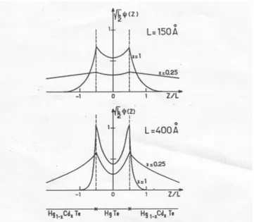
LA presented in figure 6 to illustrate the previous discussion. In figure 7 we show
the calculated
χ
1( )
z
envelope functions in Hg1 xCdxTe HgTe Hg1 xCdxTe quantumwells to illustrate the interface nature of the E1state. Although the existence of the
interface state relies only on the relative position of the I’8 edges of HgTe and
CdTe, their actual energy position, as well as their behavior at k┴≠0 (where they strongly couple to the heavy hole states), remains a subject of active research.
Fig. 7. – Dimensionless envelope functions of the ground states in Hg1 xCdxTe
HgTe Hg1 xCdxTe double heterostructures (x=1 and x=0.2) for two different HgTe
slab thicknesses.
* &
1. Duggan G., The Journal of Vacuum Science and Technology. $(1985) 1224.
2. Guldner Y., Bastard G., Vieren J.P., Voos M., Faurie J.P., Million A.,Physics Review, (+(1983) 907.
3. Yia Chung Chang, Schulman J.N., Bastard G., Guldner Y., Voods M., Physics Review, $+(1985) 2557.
5. Voisin P. Two dimensional Systems, Heterostructures and Superlattices edited by G. Bauer, F. Kuchar and H. Heinrich, Springer Series in Solid State Sci.($,Springer Verlag, Berlin, 1984, p. 192.
6. Bir G.L., Pikus G.E., Symmetry and Strain induced Effects in Semiconductors, Wiley, New York, 1974.
7. Marzin J.Y., Heterojunctions and Semiconductor Superlattices edited by G. Allan, G. Bastard, N. Boccara, M. Lannoo and M. Voods, Springer Verlag, Berlin, 1986, p. 161.
Address: