CGS Based Solar Cells with
In
2S
3Buffer Layer Deposited by CBD and Coevaporation
W. Vallejo∗ and J. Clavijo
Departamento de Qu´ımica, Universidad Nacional de Colombia
G. Gordillo
Departamento de F´ısica, Universidad Nacional de Colombia, Bogot´a, Colombia.
(Received on 29 August, 2009)
In this paper we investigatedIn2S3as substitute for CdS, which is conventionally used as buffer layer in chal-copyrite based solar cells.In2S3thin films were deposited by CBD and co-evaporation methods and these were employed as buffer layer inCuGaSe2based solar cells. Previous to the device fabrication, comparative study was carried out onIn2S3thin films properties deposited from chemical bath containing thioacetamide, Indium Chloride, and sodium citrate, andIn2S3thin films prepared by co-evaporation from its constituents elements. The influence of synthesis conditions on the growth rate, optical, structural and morphological properties of the as-grownIn2S3thin films have been carried out with Spectrophotometry, X-ray diffraction and AFM microscopy techniques. Suitable conditions were found for reproducible and good qualityIn2S3thin films synthesis. By depositingIn2S3thin films as buffer layers inCuGaSe2configuration, a maximum solar cell efficiency of 6% was achieved, whilst the reference solar cell withCdS/CuGaSe2on similar absorber exhibited 7% efficiency.
Keywords: Buffer layer,In2S3, CBD, chalcopyrite, structural properties, Solar cell.
1. INTRODUCTION
In most laboratories the standard device structure of Cu(In,Ga)Se2(CIGS)-based solar cells includes a very thin
chemical-bath-deposited (CBD) CdS buffer layer between the CIGS absorber layer and the transparent ZnO front elec-trode. At present the best results obtained with thin film based solar cells, have been achieved with solar cells fabri-cated using the structure Mo/CIGS/CdS/ZnO; the maximum efficiency reported for this type of devices is 19.9% [1]. In the last decade, serious efforts to substitute the CdS buffer layer by other nontoxic materials have been made for the fol-lowing reasons:
i) The expected environmental risks arising from imple-mentation of synthesis CdS thin film by CBD process in a CIGS module production line.
ii) The possibility to improve the light transmission in the blue wavelength region by using a material with a wider bandgap compared to CdS.
Alternative buffer layers to CdS films have been in-vestigated to fabricate Cd-free devices and enhance so-lar cell current generation. ZnS-based buffer layers, pre-pared by CBD and atomic layer deposition (ALD), have al-ready demonstrated their potential as alternative buffer ma-terial [2,3]; efficiencies up to 18.6 % have been obtained using ZnS(O,OH)/ZnO as window layer in CIGS based cells [4]. In2S3, In2Se3, ZnSe and (Zn,In)Sex layers de-posited by different methods have demonstrated to be po-tential as alternatives buffer layers in chalcopyrite based so-lar cells [5]. Efficiencies up to 15.7% have been reported to In2S3−CBD/CIGS based solar cells [6]. The best re-sults obtained to Cd-free buffer layer in CIGS based cells using materials deposited by physical methods have been achieved usingIn2Se3and(Zn,In)Sex[7,8]; efficiencies up to 15.3 % have been reported with(Zn,In)Sexdeposited by co-evaporation in CIGS based cells [8].
∗Electronic address:[email protected]
In this paper we have deposited good qualityIn2S3 thin
films by the CBD method, in this process were used thioac-etamide, Indium Chloride and sodium citrate as reagents. On the other hand, we have also found conditions for repro-ducible deposition of good quality In2S3thin films by
co-evaporation from elementals Indium and sulphur. A com-parative study of the optical, structural and morphological properties of the In2S3 films deposited by both methods
is also reported in this work. Preliminary results revealed that the performance of solar cells fabricated with structure SLG/Mo/CuGaSe2/In2S3/ZnO/Al is similar to reference
so-lar cell with CdS/CuGaSe2
2. EXPERIMENTAL
In this work theIn2S3thin films were prepared by CBD
and co-evaporation methods; special emphasis was put on finding conditions to grow In2S3 thin films by CBD with
adequate properties to be used as buffer layers inCuGaSe2
(CGS) based solar cells. Different layers constituting the de-vice were deposited as follows: The samples prepared by CBD were grown from solution containing Thioacetamide (Scharlau) (TA) and Indium Chloride (InCl3) as sources of
S2−andIn3+respectively, acetic acid (Es-Science) (HA) and sodium citrate (Riedel-de Han) (Cit) was used as complexing agents of theIn3+. theInCl3was prepared in our laboratory
using the following procedure: 67 ml of concentrated HCl and 5 drops of concentratedHNO3were added to 22.96 gr
(0.200 moles) of metallic In (99.9%, Merck). This solution was heated up until the indium was totally dissolved and the excess HCl evaporated. The resulting solution was diluted to 100mL with water distillated. TheIn2S3thin films were
grown on CGS absorbers and Indium tin oxide covered glass substrates (Kintec Co) (ITO).
TheIn2S3thin films grown by physical method were
[HA]=300mM. [Cit]=30mM; during the deposition the bath temperature was maintained at 70◦C and the solution pH in 2.5. Additionally Good quality In2S3 thin films were
obtained by co-evaporation as follows: mass ratio [Sul-phur/Indium]=7, Indium deposition rate of 2 ˚A/s, Sulphur evaporation temperature at 140◦C and the substrate temper-ature at 300◦C.
The Molybdenum (Mo) films were prepared using a DC magnetron sputtering system with an S-gun configuration electrode. The main difference of this system with the ventional planar Rf sputtering systems, is that the S-gun con-figuration employs a central anode surrounded by a Mo cath-ode (99.99% pure), which presents a conical shaped concav-ity. Details of the Mo films deposition are given in reference [10]. The zinc oxide (ZnO) films were deposited by reactive evaporation using a special procedure described elsewhere [11].
The optical, structural and morphological properties of the In2S3 thin films were studied through transmittance, XRD
and AFM measurements carried out with a Perkin Elmer Lambda 2S spectrophotometer, an X-ray diffractometer Shi-madzu 6000 and a PSI AFM microscope. The film thickness was determined using a Veeco Dektak 150 surface profiler.
3. RESULTS AND DISCUSSION
Previous to the device fabrication, it was performed a com-parative study of the deposition conditions influence on the growth rate and on the optical, structural and morphological properties of In2S3 thin films CBD and co-evaporated
de-posited.
3.1. Influence of deposition conditions on the growth rate.
a)In2S3films deposited by CBD
The influence of the preparation method and synthesis pa-rameters on the growth rate and the optical and structural properties ofIn2S3 thin films have been investigated. The
variation of the thickness of CBD depositedIn2S3thin films
as a function of: pH, [TA], [InCl3] and substrate type are
plotted in Fig. 1; this study was carried out keeping constant the others parameters as indicated above.
It is observed that the growth rate of the In2S3 films is
significantly affected by the synthesis parameters and sub-strate type. Two different regions can be distinguished dur-ing the growth process ofIn2S3thin films (see Fig. 1a), an
initial linear region and the final saturation region, which are
icantly affects the growth rate. In general, with the solution we used, theIn2S3 thin films didn’t grow directly on soda
lime glass substrates; however, this compound grown quite well on ITO covered glass substrates. It is possible that for starting the nucleation process is required the presence of some ions (Indium and/or tin) on the substrate’s surface. On the other hand, the results also show that the layers ofIn2S3
grown faster on CGS than on ITO. This behavior could be explained taking into account that the CBD growth process is affected by surface kinetic processes [12]; in particular, the chemical activity of the substrate surface seems to be the factor responsible for the differences in growth rate observed. The results of Fig. 1a, can therefore be explained assuming that the CGS layers present more chemical activity than ITO covered glass substrate for the CBD growth ofIn2S3films.
The change of the film thickness as function of molar con-centration of the reagents and the pH was studied. Fig. 1b, 1c shows that as the TA andInCl3concentration increases
the thickness of the film increases also. On the other hand Fig. 1(d) shows that growth rate of the processes increases strongly as the pH value decreases. We have found that the optical properties of theIn2S3films deposited at pH values
lower than 2.0 are poor (low transmittances) whereas those deposited at pH closer to 2.5 present good optical proper-ties. At pH values greater than 2.5 the In2S3 films were
neither uniforms nor adherents to substrate surface, because under those conditions the homogeneous reaction predom-inates in the solution. At pH of 2.5 and concentrations [InCl3]=25mM; [TA]=350mM, uniforms layers and
adher-ents to the substrate surface were obtained.
b) In2S3films deposited by co-evaporation
In Fig. 2 are compared curves of thickness vs. deposi-tion time corresponding to In2S3 thin films grown by
co-evaporation on different substrate types. It is observed that growth rate of In2S3 thin films is not affected by neither
the substrate type nor the substrate temperature. The re-sults show that unlikeIn2S3thin films deposited by CBD, the
growth rate ofIn2S3thin films deposited by co-evaporation
is independent from type substrate used; it suggests at 300◦C the diffusion and coalescence processes occurred at same time on CGS and on soda lime glass substrates. On the other hand the growth rate ofIn2S3thin films decreases by
(a) (b) (c) (d)
FIG. 1: (a) Change of thickness ofIn2S3thin films on different substrates as function of deposition time. Change of thickness ofIn2S3thin films deposited on ITO as function of concentration of: (b) [InCl3], (c) [TA] and (d) pH.
(a) (b)
FIG. 2: (a) Change thickness ofIn2S3thin films grown on different substrates as function of deposition time. (b) Change of growth rate ofIn2S3thin films grown on glass substrates as function of the substrate temperature.
3.2. Structural results
a) In2S3films deposited by CBD
TheIn2S3thin films were initially characterized through
XRD measurements in order to study the effect of the de-position conditions on the structural properties. Owing to their small thickness, the crystallinity of the films was very poor. The Fig. 3 shows XRD spectra corresponding toIn2S3
thin films deposited at different molar concentration InCl3
and TA onto ITO substrates, keeping constant the deposition time at 25 minutes and the rest of the deposition parame-ters as indicated above. Very thin samples deposited at lower InCl3and TA molar concentrations, present just two
reflec-tions at 2θ=33.7 and at 2θ=34.1◦which match well reflec-tions associated to the (001) and (200) planes of Indium ox-ide hydroxox-ide (InOOH) (JCPDS # 17-0549); thicker samples deposited at higher molar concentrations present addition-ally a third reflection at 2θ=48.37 which match quite well the reflection associated to the (2212) plane of the tetragonal β−In2S3phase (JCPDS#25-0390).
Some authors have reported results concerning CBD de-positedIn2S3thin films structure, and most of them suggest
a mixture of the cubicα andβ phases [13,14]. The pres-ence of Indium oxide hydroxide and another compounds of In2S3such asγandεphases have been also reported [14,15].
It seems that the phase in which the CBD depositedIn2S3
films grow, depends on the deposition conditions, especially type and concentration of the reactants constituting the solu-tion. The fig. 4 shows the XRD pattern corresponding to 80 nm thickIn2S3 films deposited by CBD on CGS absorber,
using a chemical bath composition described above. It is ob-served thatIn2S3thin films grown on CGS present the same
reflections than samples deposited on ITO substrates, indi-cating that structure and the phase in whichIn2S3thin films
grow are not affected by substrate type used.
FIG. 3: XRD pattern ofIn2S3thin films deposited by CBD on ITO for different molar concentration of: (a) [InCl3], (b) [TA].
b) In2S3films deposited by co-evaporation
Fig. 5 shows experimental XRD pattern corresponding to In2S3thin films deposited on soda lime glass substrates by
co-evaporation varying the substrate temperature. The XRD measurements revealed that all the as grownIn2S3thin films
were polycrystalline in nature; The diffraction peaks could be produced by crystalline planes of the tetragonalβ−In2S3
sim-
FIG. 4: (a) XRD pattern of 80 nm thickIn2S3thin films deposited by CBD on CGS. (b) XRD pattern CGS film.
ulation shows that all reflections resulting from experimental XRD measurements match quite well with reflections of a XRD pattern simulated. These results indicate thatβ−In2S3
films with adequate properties crystallines for buffer layers can be deposited by co-evaporation at temperatures around 150◦C.
The Fig. 6 shows the XRD pattern corresponding to a 110 nm thick In2S3 film deposited at 300◦C on CGS thin
film. The XRD measurements revealed thatIn2S3films
de-posited by co-evaporation on CGS films present the same reflections than the samples deposited on glass substrates, indicating that the substrate type does not affect the phase in whichIn2S3thin film grows.
3.3. Transmittance measurements
a) In2S3films deposited by CBD
Fig. 7 shows typical transmittance curves of In2S3 thin
films deposited by CBD varying the deposition time and syn-thesis parameters ([TA], [InCl3], [pH]), keeping constant the
rest of deposition parameters as indicated above.
It is observed that the transmittance in the visible region decreases as the concentration ofInCl3 increases (fig. 7a),
probably due to increasing the film thickness. On the other hand, in the high absorption region (λ<350 nm) the trans-mittance of layers synthesized at low concentration of TA (fig. 7b), does not reach zero value. This behavior seems to be caused by the presence of pores in the layer ofIn2S3,
which are generally formed in very thin films because the amount of reactive is not sufficient to start the coalescence phase of the growth process. This fact prevents the growth of In2S3 in some regions of the substrate which facilitates
the transmission of light without absorption. On the other hand at pH values lower than 2.0 the optical properties of the films were poor (fig. 7c), the slope of the transmittance
FIG. 5: Comparison of XRD pattern ofIn2S3thin films deposited by co-evaporation on soda lime glass substrate varying the substrate temperature, with one XRD pattern simulated theoretically assum-ing that sample grown in the tetragonalβ−In2S3phase.
(a)
(b)
(c)
FIG. 7: Change the spectral transmittance ofIn2S3 thin films deposited by CBD on ITO substrates as function of concentration of: (a) [InCl3], (b) [TA] and (c) pH.
curve and the magnitude of the transmittance are strongly re-duced, probably due to the formation of big clusters on the substrate, which are formed as a consequence of strong co-precipitation within the solution ofIn2S3, giving raise to big
aggregates that condense on the substrate forming clusters. b) In2S3films deposited by co-evaporation
In Fig. 8 are plotted typical transmittance curves ofIn2S3
thin films deposited by co-evaporation varying the substrate temperature between 150 and 400◦C (Fig. 8a) and the thick-ness between 80 and 800 nm (Fig. 8b). A curve of (αhν)2
vs. hν, is also shown in Fig. 8c, whereαis the absorption coefficient determined from the transmittance measurements and calculations carried out as described in reference [16]; this curve is used for determining the energy band gap Eg of theIn2S3thin film, from the intercept with the hνaxis of the
linear part of the graph (αhν)2vs hν. It is observed a shift of
the transmittance curves toward the region of lower values of λwhen the thickness decreases. We have not found a defini-tive explanation for this behavior. However, we consider that the shift of the cutoff wavelength observed could be associ-ated to changes in the band structure, induced by changes in the different interaction processes taking place during stages of the thin films growth. In particular, the superposition de-gree of electron clouds from neighboring atoms, which af-fects the band width, can be increased by increasing the film thickness. It was also found that for thicknesses greater than 1µm, the optical gap of theIn2S3thin films keeps constant.
Therefore, to prevent the effect of the thickness on the opti-cal gap Eg, a sample with thickness greater than 1µm was selected to determine this value; anEgvalue of 2.75 eV was found for theIn2S3film deposited by co-evaporation in this
work.
Comparing the transmittance curves of fig. 7b with that displayed in Fig. 8b, it is observed that the transmittance around 350 nm of CBD deposited In2S3 films, is
signifi-cantly lower than those of theIn2S3films deposited by
co-evaporation, indicating that the substrate-coverage degree of very thin CBD depositedIn2S3films is greater than the
pre-sented by co-evaporated films with similar thickness. This result indicates that the CBD method allows growingIn2S3
thin films with larger substrate coverage than samples ob-tained with similar thickness deposited by co-evaporation.
3.4. Morphological results
a)In2S3films deposited by CBD
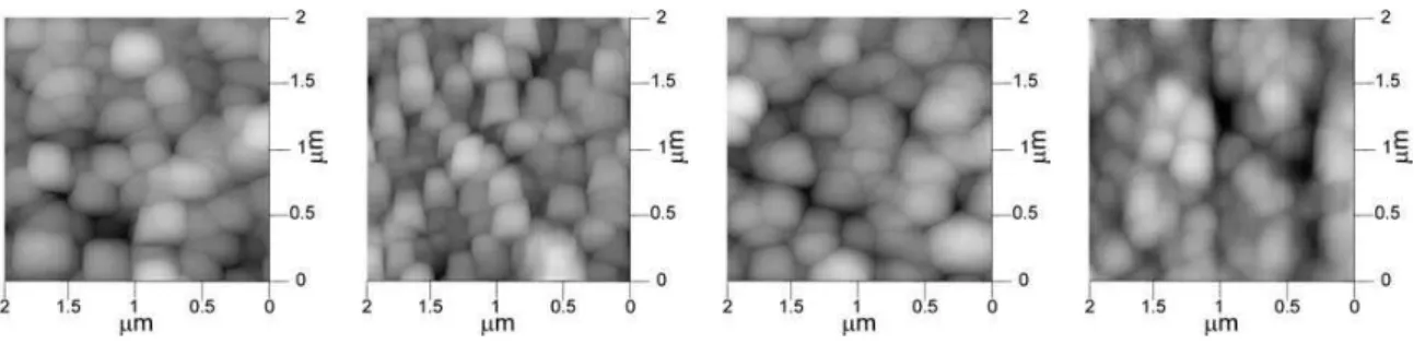
Fig. 9 shows typical AFM images of: CGS (Fig. 9a), ITO (Fig. 9b) thin films deposited on soda lime glass sub-strates, 80 nm thickIn2S3 thin film deposited by CBD on
ITO (Fig. 9c) and CGS (Fig. 9d) thin films respectively. In table 1 are listed the corresponding grain size average values, which were determined analyzing the AFM images showed in Fig. 9, through the ProScan image analysis software. It is observed that theIn2S3thin films show similar structure
with smaller crystallites that are uniformly distributed over the substrate surface, further theIn2S3thin films deposited
by CBD on ITO and on CGS covered glass substrates tend to grow with similar morphology and grain size of the substrate on which were grown.
b)In2S3films deposited by co-evaporation
Fig. 10 shows AFM images ofIn2S3thin films with
dif-ferent thicknesses deposited by co-evaporation on soda lime glass substrate (Fig 10a, b c) and AFM image ofIn2S3thin
film deposited on CGS absorber (Fig 10d). In table 2 are listed the corresponding average values of the grain size and the average surface roughness, obtained for the samples whose AFM images are shown in Fig. 10.
It is observed that the grain size of theIn2S3thin films
FIG. 8: Change of Spectral transmittance ofIn2S3thin films deposited by co-evaporation as function of: (a) temperature substrate. (b) deposition time. (c) (αhν)2vs.hνspectra indicating the value of Eg.
FIG. 9: AFM images corresponding to: (a) CGS substrate, (b) ITO substrate, (c) 80 nm thickIn2S3film deposited by CBD on CGS and (d) 80 nm thickIn2S3film deposited by CBD on ITO.
TABLE 1: Grain size average values derived from images displayed in Fig. 9.
Grain size average values derived from images displayed in Fig. 9.
Sample Glass/ITO
Glass/CuGaSe
2Glass/CGS/ In
2S
3Glass/ ITO/ In
2S
3Grain size (nm)
190
230
215
185
crystallites are produced, for shorter deposition time inter-vals the films with smaller crystallites are not able to grow into bigger ones (fig.10a), whereas for thicker films (fig.10c) the crystallinity of the film crystallites grew bigger. The AFM measurements also revealed that theIn2S3 thin films
surface topography of the as-grown layers varied with film thickness. The average surface roughness ofIn2S3films
de-posited on glass substrate increased from 1.5 nm to 2.5 nm with increase of film thickness (table 2). The increase of surface roughness with thickness is associated with the in-crease of grain size in the films. However, as film thickness increases the grain size was increased along with the surface roughness, which indicates the 3D growth in the films.
3.5. I-V measurements
The device performance was analyzed by J-V measure-ments carried out under AM 1.5 irradiance (100 mW/cm2).
Fig. 11 plots J-V curves corresponding to the best CGS based solar cells fabricated withIn2S3buffer layer deposited
by CBD or co-evaporation, as well as the J-V curve of a reference cell fabricated using a CBD deposited CdS layer as buffer. The In2S3 and the CdS buffer layers were
de-posited on the CGS absorber prepared in the same run with [Ga]/[In]∼1.2. In table 3 the output parameters of the best solar cells fabricated usingIn2S3buffer layers are compared
with those of a reference solar cell fabricated with CBD de-posited CdS buffer.
In general, the cells fabricated in this work are character-ized by rather low open circuit voltage Voc; we observed that in the best case, the Voc/Eg ratio is around 0.47, which is much lower than that of high efficientCu(In,Ga)Se2(CIGS)
FIG. 10: AFM images ofIn2S3films deposited by co-evaporation on glass substrates with different film thickness: (a) 110nm, (b) 180 nm, (c) 760 nm. (d) AFM image of a 110 nm thickIn2S3film deposited on CGS.
TABLE 2: Grain size average and roughness values derived from images displayed in Fig. 10.
Grain size average and roughness values derived from images displayed in Fig. 10.
Sample Glass/
In
2S
3Glass/
In
2S
3Glass/
In
2S
3Glass/CGS/
In
2S
3In2S3 - thickness (nm) 110 180 760 110
Grain size (nm) 110 170 200 210
Roughness Rms (nm) 1.5 2.0 2.5 5.0
at a very high density, as well as inCu(In,Ga)Se2 alloys
with high Ga contents [17]. The increase in bulk recom-bination leads a decrease in both short circuit current and the electron’s diffusion length, which give rise to a decrease of the Voc [18]. Other reason for the large differences in Eg/q−Voc in CGS devices compared with high efficiency CIGS based solar cells, is the increase of the band offset at the absorber/buffer interface by increasing the Ga content of the absorber. It is also observed that the FF of CGS based cells is less than 0.62, which is significantly lower than the efficiency CIGS (>0.77). The low values of FF of CGS based cells arise as a consequence of high series resistance values (>10Ω) and low shunt resistance values (<800Ω).
The results of Fig.11 show that the Voc, Isc and FF val-ues of the cells fabricated with co-evaporatedIn2S3 buffer
are significantly lower than those of the other devices fab-ricated in this work; this behavior seems to be caused by interdiffusion ofIn2S3 into the absorber during its growth,
because this layer is deposited around 3000C, whereas the
CBD deposited layers are grown at 700C. The interdiffusion
ofIn2S3reduces the shunt resistance of the device and
dete-riorates the hetero-interface with the CGS absorber; leading to an increase of the interface recombination. The very low Voc and Isc values obtained with solar cells fabricated using co-evaporatedIn2S3buffer, suggest that the interface
recom-bination is the predominant loss mechanism of photocurrent in this type of devices and the mechanism responsible for the additional reduction of Voc observed in the cells fabricated with co-evaporatedIn2S3buffer.
4. CONCLUSIONS
Conditions for reproducible deposition ofIn2S3thin films
by CBD with adequate properties to be used as buffer layer in CGS based solar cells were found. XRD studies revealed that the deposition parameters of CBD depositedIn2S3films
affect the phase in which they grow; on the contrary, the
FIG. 11: J − V Characteristics of CuGaSe2/CBD-CdS, CuGaSe2/CBD-In2S3 and CuGaSe2/coevaporated-In2S3 based solar cells.
XRD measurements indicated that in the range studied, the co-evaporated In2S3 films always grow in the tetragonal
β−In2S3phase, independently of the synthesis parameters
Spectral transmittance measurements revealed that very thinIn2S3films deposited by CBD present greater substrate
coverage than those of similar thickness deposited by co-evaporation. It leads to building solar cells with higher pho-tocurrent values.
In general, the cells fabricated in this work are character-ized by rather low open circuit voltage values, which could be attributed to bulk recombination via states generated by intrinsic defects induced by a lattice mismatch between the surface layer and the bulk material that arises in CGS at a very high density. The results also revealed that the perfor-mance of CGS based solar cells fabricated using CBD
de-fabricated with CBD deposited CdS buffer layer and better than performance obtained with CGS based solar cells fab-ricated using coevaporation depositedIn2S3. The best
effi-ciency was 6% for cells withIn2S3 buffer and 7% for cells
with CdS buffer.
Acknowledgements
This work was supported by Colciencias (Contract #247-08) and DIB-Universidad Nacional de Colombia.
[1] I. Repins, M.A. Contreras, B. Egaas, C. DeHart, J. Scharf, C. L. Perkins B. To, R. Noufi. “Short Communication: Accel-erated Publication: (199)-efficient ZnO/CdS/CuInGaSe2 so-lar cell with (812) fill factor”.Progress in Photovoltaics: Re-search and Applications, 16, 2008, pp. 235-239.
[2] Naghavi N, C. Hubert, V. Bermudes, B. Cavana, A. Etcheberry, D. Hariskos, M. Powalla, D. Lincot, O. Kerrec, “From CdS to Zn(S,O,OH) : a better understanding of chemi-cal bath deposition parameters and cells properties using elec-trodeposited CuIn(S,Se)2 and coevaporated Cu(In,Ga)Se2 absorbers”. In21st European Photovoltaic Solar Energy Con-ference, Dresden, Germany (2006) 1843.
[3] Ennaoui, A, M. Bar, J. Klaer, T. Kropp, R. Sez-Araos M.C. Lux-Steiner, “New Chemical Route for the Deposition of ZnS Buffer Layers: Cd-freeCuInS2-based thin film solar cells with efficiencies above 11%”. In20th European Photovoltaic Solar Energy Conference, Barcelona, Spain (2005) 1882.
[4] M.A. Contreras, T. Nakada, M. Hongo, O.A. Pudov and J. R. Sites, “ZnO/ZnS(O,OH)/Cu(In,Ga)Se2/Mo solar cell with 18.6% efficiency”3rd World Conference on Phorovoltaics En-ergy Conversion, Osaka. Japan (2003).
[5] D. Hariskos, S. Spiering, M. Powalla, “Buffer layers in Cu(In,Ga)Se2 solar cells and modules”, Thin Solid films 480– 481 (2005) 99–109.
[6] D. Hariskos, M. Ruckh, U. Rqhle, T. Walter, H.W. Schock, J. Hedstrfm, L. Stolt, ‘A novel cadmium free buffer layer for
Cu(In,Ga)Se2based solar cells’, Solar Energy Materials and Solar Cells 41–42 (1996) 345.
[7] A. Ennaoui, S. Siebentritt, M.Ch. Lux-Steiner, W. Riedl, F. Karg, ‘High-efficiency Cd-free CIGSS thin film solar cells with solution grown zinc compound buffer layers’, Solar En-ergy Materials and Solar Cells 67 (2001) 31.
[8] S. Chaisitsak, Y. Tokita, H. Miyazaki, R. Mikami, A. Yamada, M., Konagai, ‘Control preferred orientation forCu(InGa)Se2 thin films and its effect on solar cell performance’, Proceed-ings 17th European Photovoltaic Solar Energy Conference, Munich, Germany, 2001, pp. 1011.
[9] E. Romero , J. Clavijo, J.S. Oyola and G. Gordillo, “ Effect of synthesis parameters on the optical and structural properties ofCuGaSe2thin films”, Rev. Mex. De F´ısica, S 53 (7) (2007) 265-269.
[10] G. Gordillo, F. Mesa and C. Calder´on, “Electrical and Mor-phological Properties of Low Resistivity Mo thin Films Pre-pared by Magnetron Sputtering”, Brazilian Journal of Physics, vol.36 , No.3B (2006) 982-985.
[11] G. Gordillo,C. Calder´on, J. Olarte y H. Mndez, “Preparation and Characterization of ZnO thin Films deposited by Reactive Evaporation”, Proc. 2nd World Conference on Photov. Solar Energy Convertion, Vienna-Austria (1998) pp 750.
[12] M. Froment, D.Lincot. ‘Phase formation processes in solu-tion at the atomic level: metal chalcogenide semiconductors’,
Electrochem. Acta.40, (1995) pp. 1293-1303.
[13] C.D. Lockhande, A. Ennaoui, P.S. Patil, M. Giersig, K. Dies-ner, M. Muller, H. Tributsch, ‘Chemical bath deposition of indium sulphide thin films: preparation and characterization’, Thin Solid Films 340 (1999) 18.
[14] R. Bayon, J. Herrero: “Structure and morphology of the in-dium hydroxy sulphide thin films”, Appl. Surf. Sci 158 (2009) 49–57.
[15] L. Lyudmila, K. Kim, K. Yoon, M. Konagai, A. Byung. “Thin film CIGS-based solar cells with an In-based buffer layer fab-ricated by chemical bath deposition”,3rd World Conference on Photovoltaics Energy Conversion, Osaka. Japan (2003). [16] R Swanepoel ‘Determination of the thickness and optical
con-stants of amorphous silicon’. J. Phps. E: Sci. Instrum.. Vol. 16, 1983.
[17] M.A Contreras, H. Wisner, J. Tuttle, K. Ramanathan and R. Noufi, “Issues of the chalcopyrite/defect-chalcopyrite junction model for high-efficiencyCu(In,Ga)Se2 solar cells”, Solar Energy Mat. Solar Cells 49 (1997) 239-247.

![Fig. 7 shows typical transmittance curves of In 2 S 3 thin films deposited by CBD varying the deposition time and syn-thesis parameters ([TA], [InCl 3 ], [pH]), keeping constant the rest of deposition parameters as indicated above.](https://thumb-eu.123doks.com/thumbv2/123dok_br/18983556.457977/4.871.87.412.89.394/transmittance-deposited-deposition-parameters-constant-deposition-parameters-indicated.webp)
![FIG. 7: Change the spectral transmittance of In 2 S 3 thin films deposited by CBD on ITO substrates as function of concentration of: (a) [InCl 3 ], (b) [TA] and (c) pH.](https://thumb-eu.123doks.com/thumbv2/123dok_br/18983556.457977/5.871.120.769.77.404/change-spectral-transmittance-films-deposited-substrates-function-concentration.webp)