Characterization of CBD-CdS Doped with Some Rare Earths III (Eu
3+,Ce
3+) as Function of
Synthesis Time
Mariana Enelia Linares-Avilésa, Jorge Indalecio Contreras-Rascónb, Joel Díaz-Reyesc*, Javier
Martínez-Juárezd, Roberto Saúl Castillo-Ojedae, Miguel Galván-Arellanof, José Abraham
Balderas-Lopeza, Mario Álvarez-Ramosb
Received: July 06, 2017; Revised: October 13, 2017; Accepted: December 23, 2017
Rare earths (Europium, cerium)-doped CdS nanofilms are prepared using the growth technique chemical bath deposition (CBD) at the reservoir temperature of 70±2°C varying the synthesis time in a wide range. For the rare earths doped CdS nanofilms the synthesis time was ranged from 80 to 135 min. The rare earths molar concentration was in the range 0.0≤x≤3.47, which was determined by energy dispersive X-ray spectroscopy (EDS). The X-ray diffraction (XRD) analysis reveals that CdS nanofilms showed the zinc blende (ZB) crystalline phase. The nanocrystal size was ranged from 2.67 to 2.35 nm for the CdS and 1.84-2.33 nm for rare earth-doped CdS that were determined by the Debye-Scherrer equation from ZB (111) direction and it was confirmed by transmission electron microscopy (TEM). The doped CdS exhibits a direct band gap that diminishes with the increase of the synthesis time, from 2.50 to 2.42 eV, which was obtained by transmittance. The room-temperature photoluminescence of CdS presents the band-to-band transition at 431 nm, which is associated with quantum confinement because the grain size is less than its Bohr exciton radius and a dominant band at 523 nm, which is called the optical signature of interstitial oxygen. Eu3+-doped CdS photoluminescence
shows the dominant radiative peak at 576 nm that is associated to the intra-4f radiative transition of
Eu3+ ions, which corresponds to the magnetic dipole transition, (5D 0→
7F1). For the Ce3+-doped CdS the
dominant radiative transitions are clearly redshifted. Additionally, other radiative peaks associated at structural defects are observed. The passivation of the CdS by rare earths was approximately of two orders of magnitude obtaining better results with cerium.
Keywords: Chemical bath deposition, CdS, Nanocrystals, Synthesis time, Rare earths, europium, cerium.
* e-mail: [email protected]
1. Introduction
Semiconductor nanostructures have attracted a lot of
attention due to their unique optical, electronic mechanical and properties. Inorganic compounds doped with lanthanide ions are widely used as the luminescent materials in lighting1
and displays2, optical amplifiers3 and lasers4. Recently, the
optical properties of nanocrystals doped with lanthanide
impurities have attracted much attention because of they are
expected to modify both electronic states and electromagnetic fields. Therefore, a possible influence of quantum size effect on the luminescence properties is expected for II-VI
semiconductor nanocrystals due to the inclusion of rare earth (RE) metal ions5. The effects of the quantum-confinement
size of the semiconductor nanoparticles not only create photogenerated carriers, which may have an interaction with f-electrons but also significantly influence the optical aUnidad Profesional Interdisciplinaria de Biotecnología, Instituto Politécnico Nacional, Av. Acueducto
de Guadalupe S/N, Gustavo A Madero, Barrio La Laguna Ticomán, Ciudad de México, 07340, México
bDivisión de Ciencias Exactas y Naturales, Departamento de Física, Universidad de Sonora, Col.
Centro, Hermosillo, Sonora, 83000, México
cCentro de Investigación en Biotecnología Aplicada, Instituto Politécnico Nacional, Ex-Hacienda de
San Juan Molino, Km. 1.5, Tepetitla, Tlaxcala, 90700, México
d Centro de Investigación en Dispositivos Semiconductores, Benemérita Universidad Autónoma
de Puebla, 14 Sur y Av. San Claudio Edif. 103C, Ciudad Universitaria, Col. San Manuel, Puebla, 72570, México
eUniversidad Politécnica de Pachuca, Km. 20, Rancho Luna, Ex-Hacienda de Santa Bárbara,
Municipio de Zempoala, Hidalgo, 43830, México
fDepartamento de Ingeniería Eléctrica, SEES, CINVESTAV-IPN, Apartado Postal 14-740, Ciudad de
properties6. Excitonic transition in the host material and an
improvement in the luminescence intensity are also expected
for the semiconductor nanostructures after the rare earths
(RE) doping. The effects of the reduced dimensionality on the electronic relaxation and the phonon density-of-states of semiconductor compounds and insulating nanocrystals have been extensively investigated by both theoretical and experimental approaches7,8.
Doping of II-VI compounds with lanthanides ions like cerium, terbium and europium, etc., has been extensively
studied9. Doping of rare earth element like cerium reduces
the particle size of nanomaterials and increases surface area10.
Vij et al. reported the luminescence studies on Ce doped SrS nanostructures and Ce doped CaS nanoparticles synthesized by solid state diffusion method11. Other authors have reported
luminescence investigations on Ce3+-doped CaS synthesized
using the chemical co-precipitation method12.
The Chemical bath deposition (CBD) method is one of the cheapest methods to deposit thin films and nanomaterials, as it does not depend on expensive equipment and is a scalable technique that can be employed for large area batch processing or continuous deposition. The major advantages of CBD is that it requires only solution containers and substrate mounting
devices and it is friendly to the environment because of the
deposition of the films is carried out at low temperatures. The one drawback of this method is the wastage of solution after every deposition. Among various deposition techniques,
chemical bath deposition yields stable, adherent, uniform
and hard films with good reproducibility by a relatively simple process. The chemical bath deposition method is one of the suitable methods for preparing highly efficient thin films in a simple manner. The growth of thin films strongly depends on growth conditions, such as duration of
deposition, composition and temperature of the solution, and
topographical and chemical nature of the substrate. Deposition by chemical bath technique of thin films consists of moderate release of metal ions into alkaline solution13. This technique
has become important for the development of thin film solar cells, since the synthesis of CdS by this method offers a better efficiency than traditional evaporation method14-16. In
the deposition of the thin film by CBD technique exhibits two different mechanisms: The first mechanism is that involving the reaction of atomic species on the surface, this
mechanism is called ion-to-ion17-19 and the second mechanism
is associated with the agglomeration of colloids formed in the solution, which can be regarded as an increase in grouping or cluster-by-cluster. For practical purposes, the formation of the core, which leads to the formation of the film, it can occur by a process of heterogeneous nucleation on the substrate or through a process of homogeneous nucleation in the volume of the solution.
In this work reports the synthesis and structural and optical characterization of CdS and CdS:(Ce3+, Eu3+)
nanofilms obtained by chemical bath deposition on glass
substrates at low temperature and at different synthesis times. The effects of the chemical composition on structural and
optical properties of the CdS and CdS:(Ce3+,Eu3+) alloys were
studied by EDS, X-ray diffraction, HRTEM, transmittance and room- temperature photoluminescence.
2. Experimental details
The chemical bath deposition is a technique to deposit films on a solid substrate from a reaction that occurs in solution. It starts from an aqueous solution of salts of the elements of the compound to be obtained. It requires that the compound
to deposit is relatively insoluble and chemically stable in the
solution to give a simple precipitation in an ionic reaction20.
The method of obtaining of CdS doped with rare earth was
the chemical bath deposition in its modality of immersion,
in which a cryo-thermostat of circulation Polyscience with temperature controller of -40 to 200°C was used. Being graded it to the temperature of 20°C to avoid the release of harmful gases into the environment and using ammonium nitrate as complexing agent. The solutions mixture is carried out using the following precursors: cadmium chloride
dehydrate (CdCl2+2H2O) (Productos Químicos Monterrey S.
A.), potassium hydroxide (KOH) (JT Baker, 98.6% purity), Ammonia Nitrate (NH4(NO3)) (Sigma-Aldrich, 99.5% purity)
and thiourea thiocarbamide (Fermet, 99.9% purity). The nitrifying reagents are Europium (III) nitrate pentahydrate
(Eu(NO3)3+5H2O) (Sigma-Aldrich, 99.999% purity) and Cerium
(III) nitrate (Ce(NO3)3+6H2O) (Sigma-Aldrich, 99.999%
purity) working with the following concentrations 0.05 M
CdCl2, 0.05 M KOH, 0.1 M NH4(NO3), 0.05 M NH2SCNH2.
The used precursors concentrations are Eu(NO3)3 0.001 M
and Ce(NO3)3 0.001 M with the appropriate volumes, the
doping is achieved when the solutions mixture has a slightly basic pH. The synthesis time was ranged from 60-75 min for single CdS, 80-135 min for doping by lanthanide impurities, achieving yellowish-opaque surfaces. The number that
accompanies the name of the sample corresponds to the
time of synthesis, for example the sample C60 indicates that it was synthesized during 60 min. The CdS:(0,Eu3+,Ce3+)
a He-Cd (Omnichrome-Series 56) laser emitting at 325 nm with an optical excitation power of ~15 mW at room temperature. The radiative emission from the sample was focalized to the entrance slit of a HRD-100 Jobin-Yvon double monochromator with a resolution better than 0.05nm, and detected with an Ag-Cs-O Hamamatsu photomultiplier with a spectral response in the range 350-1000 nm.
3. Experimental Results and Discussion
The chemical stoichiometry of the CdS (or CdS:RE3+)
nanofilms was estimated by EDS measurements that besides allowed to know the presence of the residual impurities in the samples along with cadmium and sulphur. EDS spectra
indicate that samples in addition to silicon, potassium, calcium,
sodium and oxygen contain a significant amount of other
residual impurities and besides the doped samples contain
rare earths. In the subsequent to the samples CdS:(Ce, Eu) will be denominated like CdS:RE to simplify the notation. Consequently, the most of residual impurities detected in the nanolayers come from of the substrate. It has found that oxygen ions are present in synthesised samples in the form
of O2- ions that may produce CdO21. Oxidation of CdS to
CdO occurs at high temperatures as has been reported22, in
this case the temperature is low during synthesis and air drying, the conversion may have happened only at a very low percentage so that its presence could not be detected by X-Ray diffraction. However, these oxygen ions can form trap levels in the band gap, resulting in several transitions contributing or affecting to luminescence. Therefore, it appears that oxygen ions have replaced sulphurs at some
random points of the CdS (CdS:RE3+) lattice. The results of
EDS measurements are presented in Table 1, in which are included the atomic and mass percentages of the elements. The number that accompanies the sample name corresponds to the synthesis time. From the table can be seen that the nanolayers are not stoichiometric for the investigated synthesis time interval. From these results is observed that sample C60 is not a stoichiometric compound and that starting from it a higher synthesis time (higher thiourea concentration in the solution) gives a higher presence of cadmium and an absence of sulphur. Considering that each CdS unit cell contains two cadmium atoms and two sulphur atoms, since the crystalline phase of the synthesised CdS is zinc blende, as was obtained by X-ray diffraction, which will be discussed extensively later. The atomic weight of the ideal unit cell is ~288.95 that corresponds to 22.19% sulphur atoms and 77.81% cadmium atoms. Therefore, when it occurs a deviation of
the stoichiometric composition of the ideal unit cell could
establish a relationship between vacancies or interstices of the elements of the crystalline lattice (VS, VCd, Cdi, Si). In
the case of C65, which has excess of Cd and absence of
S that is indicative that cadmium is interstitial and there
are sulphur vacancies. The average errors with that were
calculated percentage masses of different elements were for cadmium 1.25%, sulphur 0.35%, europium 0.25% and for cerium 0.30%. As can be seen in Table 1, these errors do not significantly alter the found results. Table 2 shows that the samples contain a lower concentration of sulphur, indicating that have a high concentration of sulphur vacancies. Also. It can induce that there is a high concentration of cadmium and RE interstices. Therefore, in the synthesised samples; there is excess elements II and lack element VI.
Figure 1 shows X-ray diffraction patterns of CdS:RE nanofilms synthesised at different times at a temperature of 70±2°C. It is observed from diffraction patterns that CdS and
CdS:RE3+ nanofilms are in polycrystalline nature. It can be
observed that each peak corresponds fairly well with data of CdS marked in the software DICVOL04 data. The structural parameters obtained with the software DICVOL04 data are in good agreement with the published ones elsewhere23.
From this close agreement, it is confirmed that as-deposited
CdS:RE3+ nanofilms for all the used synthesis times and
precursor concentrations belong to face-centered cubic system (fcc). The X-ray diffraction patterns of CdS and CdS:RE3+
nanofilms are described in the Fm-3m(225), whose lattice
parameters were calculated using the software DICVOL04, obtaining the lattice parameter value for C60: a = 5.76 Å,
which is in agreement with the reported values23-25. As has
been reported Cadmium sulphide exists in two crystalline phase modifications: the wurtzite (WZ)26 and zinc blende
(ZB) phase25. As can be seen in Fig. 1, the obtained X-ray
diffraction patterns of the samples show clearly a predominant peak at 2θ = 26.8°, which can be assigned to (111) plane of CdS ZB crystalline phase. Additionally, the intensity weak of peak at 2θ = 28.3° is due to the diffraction from the (101) plane WZ phase whereas at 2θ = 26.4° position can be co-occupied by the (111) plane of ZB phase as well as the (002) plane WZ. However, the maximum peak intensity for both crystalline phases are different, ZB maximizes at
2θ = 26.8° corresponding to the (111) plane, whereas WZ
crystalline phase has its maximum intensity peak at 2θ = 28.2° corresponding to (101) plane27. The diffraction peaks
observed in the 15-17° range are the peaks associated with
the rare earths incorporated at the sub-lattices sites of Cd2+,
as can be seen from the diffractograms. It has been reported
in the literature that the probability that CdS dissolves in the RE2S3 (III) lattice at room temperature is very low28 but when
increases the synthesis time also is increased the probability. From XRD patterns can be assured that the RE3+ forms RE
2S3
according to the peak located at 2θ~15-17°. From the XRD
study can infer that the formation of the CdS:RE3+ occurs
in the early stage, following by the formation of RE2S3
nanocrystallites in the stage of the film growth29. Additionally,
Table 1. It presents the CdS:RE3+ films grown and the doping volume added to each one. The Cd, S and RE concentrations in the samples
were estimated by EDS. The average errors with that were calculated percentage masses of different elements were for cadmium 1.25%, sulphur 0.35%, europium 0.25% and for cerium 0.30%. For a stoichiometric compound (CdS), the percentage atomic masses are cadmium 77.81% and 22.19% sulphur. The number that accompanies the sample name corresponds to the synthesis time.
Sample RE(NO3)3 Added volume (ml)
Cd mass
weight (%) fraction (%)Cd molar fraction (%)S mass fraction (%)S molar fraction (%)RE mass fraction (%)RE molar
C60 --- 80.66 54.32 19.34 45.68 ---
---C65 --- 79.20 52.06 20.80 47.94 ---
---C70 --- 78.31 50.74 21.69 49.28 ---
----C74 --- 77.11 49.01 22.89 50.99 ----
----Eu(NO3)3 Eu Eu
Eu105 1 80.62 56.79 17.16 42.36 2.23 0.85
Eu115 2 80.25 57.12 16.71 41.70 3.04 1.18
Eu125 3 78.98 56.87 16.37 41.32 4.65 1.81
Eu135 4 71.06 43.10 22.54 47.57 5.86 3.47
Ce(NO3)3 Ce Ce
Ce80 1 74.55 46.45 24.24 52.95 1.21 0.60
Ce100 2 75.64 48.01 23.06 51.32 1.31 0.66
Ce130 3 71.06 44.03 25.26 54.32 3.68 1.65
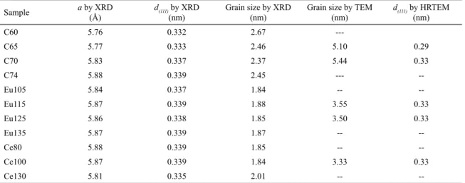
Table 2. Mean grain size of the nanofilms obtained by the Debye-Scherrer equation for the ZB (111) preferred direction showing their
dependence on the synthesis time. In addition, it presents the grain sizes obtained by TEM. Additionally, the interplanar distance estimated by X-ray diffraction and by HRTEM are shown.
Sample a by XRD(Å) d(111)by XRD
(nm)
Grain size by XRD
(nm)
Grain size by TEM
(nm)
d(111)by HRTEM
(nm)
C60 5.76 0.332 2.67
---C65 5.77 0.333 2.46 5.10 0.29
C70 5.83 0.337 2.37 5.44 0.33
C74 5.88 0.339 2.45 ---
--Eu105 5.84 0.337 1.84 --
--Eu115 5.87 0.339 1.88 3.55 0.33
Eu125 5.86 0.338 1.85 3.50 0.33
Eu135 5.87 0.339 1.87 --
--Ce80 5.88 0.339 1.85 --
--Ce100 5.87 0.339 1.84 3.33 0.33
Ce130 5.81 0.335 2.01 --
--they do not produce a mismatch in the lattice parameters
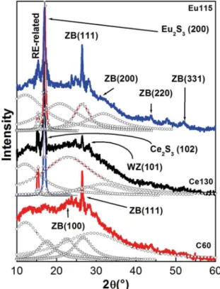
of layers, so the first case does not happen. Therefore, this can occur due to the small size of the crystals and by presence of strains that possess multiple facet diffraction peaks, which is the result of multidirectional growth of the synthetized nanocrystals. The peaks do not match exactly with the reported plane spacing for ZB and WZ phases that can be explained by the broadening of peaks, see Fig. 2. In the case of extremely small particles, where the contribution of surface free energy is very important, some deviations cannot be excluded. Fig. 2 shows the deconvolution of X-ray diffractograms of three typical samples C60, Ce130 and Eu115, to find all the diffraction peaks that make up the X-ray diffraction diffractograms. The crystallite sizes (D(hkl)) were
calculated from the line broadening of the X-ray diffraction peaks at 2θ using the Debye-Scherrer equation. The lattice parameters of CdS and the mean grain sizes are presented in Table 2. Fig. 3 shows the variation of the size of the average crystalline domain with the incorporated REs as function of synthesis time obtained by the Debye-Scherer equation through the measurement of the width at half-maximum (FWHM) of the peak of the preferential ZB (111) direction of each deposited layer. In fact, to apply the Debye-Scherrer equation30 finds that the crystalline domain presents clearly
two behaviours: a) as the synthesis time increases for single CdS the average grain size diminishes slightly from 2.67 to 2.35 nm. b) For RE3+-doped CdS there is a noticeable
there is a light increased from 1.85 to 2.03 nm for Ce and 1.84 to 1.87 for Eu by increasing the synthesis time, where
clearly is observed the RE3+ ions effect to replace Cd3+ ions
of the CdS lattice. Similar behaviour is observed for the lattice constant, as is shown in the inset of Fig. 3, for single CdS lattice constant increases lightly as synthesis time is increased, from 5.76 to 5.88 nm, and for the samples doped with cerium (europium) increases (decreases) lightly. For the interplanar distance (ID) (111) of the ZB phase is presented in Table 2, which increases lightly and was calculated from the 2θ peak position versus synthesis time. This ID, in practice, coincides with (111) ID of the ZB crystalline phase. It is worth-noting the values of electronegativity for Ce (1.12), Eu(1.2) and Cd (1.69), which are favourable to
form a solid solution31.
Figure 1. XRD diffraction patterns for CdS and CdS:RE3+ nanofilms
Figure 2. a) It shows the C60 diffractogram that displays peaks at:
2θ = 26.8, 44.2 and 52.4°. These are related to the (111), (220) and
(311) reflection planes for the ZB phase of the CdS, respectively. b) and c) They illustrate the CdS:RE3+ diffractograms, in which
clearly are shown peaks associated at RE ranged from 15-17°. All the diffraction peaks can be perfectly matched to the reference patterns (JDDC 0531447) displaying the ZB crystalline phase
Figure 3. It illustrates the grain size as function of synthesis time
for single CdS and RE-doped CdS. The inset shows the lattice parameters for undoped and doped CdS. The dash lines are some figures-of-merit for following the behaviour of experimental points
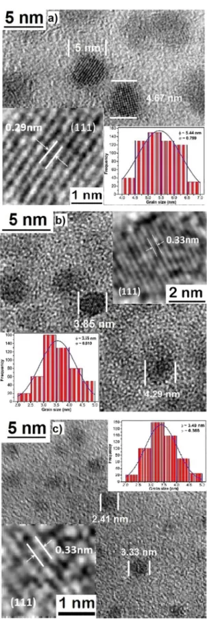
The TEM measurements of the obtained samples corroborate the presence and the nanometric size of particles. In Fig. 4 is shown some TEM micrographs of typical samples, it is evident the presence of particles with almost completely spherical shape at nanometric scale. Based on more than 100 measurements taken from the TEM micrographs of the typical samples a size distribution histogram was obtained, which are shown in the inset of Fig. 4, and it can be detected a Gaussian adjustment with a narrow distribution of size and a maximum value of 5.44 and 3.55 nm, for single CdS
and CdS:Eu3+. Absence of bimodal size distribution in the
size distribution histograms suggests that the nanoparticles
obtained by the synthesis process at different times correspond
to the formation of an CdS:RE3+ system and not the physical
mixture of nanoparticles sizes. A comparable analysis was
performed for some of the samples and the results are listed
single CdS. Therefore, the reaction time can be used to control the formation and size of the CdS nanoparticles. As can be observed in Table 2, the particle size values obtained from the X-ray diffraction using Debye-Scherrer equation and those measured from the TEM micrographs have small discrepancy. These small discrepancies in particle size is due to some approximations involved in the calculations using the Debye-Scherrer equation or coalescence of nanocrystals during preparation for TEM analysis. With the purpose of verifying the structure's quality and crystalline phase of the obtained semiconductor nanoparticles, HRTEM images were taken and the results are included in the inset of Fig. 4, which are the result of the processing of the HRTEM image using filters in Fourier space. From the HRTEM micrograph
of typical samples, it is clearly observed the formation of
nanoparticles with a defined crystalline structure, zinc blende. Amplifying and analysing the selected area of the micrograph (it is shown as insets in Fig. 4), it was possible to calculate the interplanar distances of ~0.33 nm corresponding to plane (111) of particles of crystallized CdS in blende zinc type crystalline phase. As can be seen, the results obtained by HRTEM are in good agreement with the results calculated from X-ray diffraction.
It can be seen in Fig. 3 the single CdS grain size decreases as synthesis time increases, suggesting the formation of
a solid solution as has been reported10, having a region
of discontinuity when is added RE3+ molar concentration
(V[RE3+]), the grain size decreases markedly as is observed
in figure. It remains almost constant for higher synthesis times, that is similar to a higher V[RE3+]. Moreover, the
lattice constant increases lightly with increasing synthesis time and happens a discontinuity when is added V(RE3+) in
the film, which is an effect of RE3+ substituting Cd2+ in CdS
lattice. A possible explication to this experimental fact can be due to difference of the ionic radii of Cd2+(0.97 Å) and
Ce3+(1.15 Å) and Eu3+(1.09 Å). The (111) ID of ZB cubic
phase in bulk is 0.3367 nm, this value is light lower than the ID values found for the CdS-CdS:RE films in this work. It is probable that ID values in CdS:RE3+ films are owing to the
existence of Cd2+ vacancies. For a relative low concentration
of RE3+ ions, this can be, in a large majority, be situated in:
(a) Cd2+ vacancies sites that otherwise would be empty32, (b)
in Cd2+ sites provoking the appearing of Cd2+ interstitial, and
(c) in interstitial positions. For higher synthesis times, that is higher V(RE3+), the material behaves like a solid solution,
the generation of Cd2+ vacancies, whose creation is needed to
charge balance, starts to be important in number and given
the relative ionic radius of S2-. There is a tendency of the
Full Width at Half Maximum (FWHM) of (111) peak of the growth films probably due to all of the possible RE3+ species
present in Cd2+ sites and interstitials positions33, and also to
the existence of RE2S3, which distort the crystalline lattice
and provoke disorder. The distortion produces a strong strain
Figure 4. HRTEM micrographs of the typical CdS samples: a) C60,
that affects the interatomic distances; this similar fact has
been reported23,34. In this work, the strain and distortion of
the lattice can be smaller. The appearing of S2- ions into the
material favours the relaxing of the lattice.
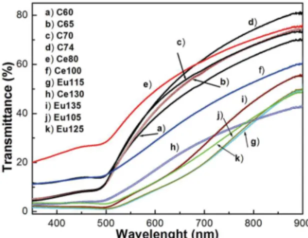
The effect of doping by rare earths on the optical properties of CdS nanolayers was investigated by room
temperature transmittance measurements as a function of
the synthesis time. The transmittance spectra in the visible and infrared ranges are recorded for the CdS:RE3+ nanofilms
in the wavelength range 350-900 nm at room temperature, see Fig. 5. The effect of V(RE3+) added in the nanofilms on
the optical properties including percentage of transmittance (% of T) and fundamental band gap (Eg) were studied in
detail. The C60 sample transmittance measured in the visible range varies from zero to almost 86.5% (without considering the substrate contribution) and is the largest of all measured transmittance spectra. The sharp reduction in the transmittance spectra at the wavelengths lower than 500 nm is due to the fundamental absorption edges of the different films. The CdS:RE3+ nanofilms were transparent,
with no observable blue colouration under our experimental conditions. The intrinsic absorption edge of the CdS nanofilms can be evaluated and discusses in terms of the indirect interband transition. As is well-known the optical band gap (Eg) of a semiconductor material is related to the
optical absorption coefficient (α) and the incident photon energy (E). The α for a film of thickness d and reflectance R is determined near the absorption edge using the simple
relation: α = ln{(1-R)2/T+[((1-R2)/2T)2+R2]1/2}/d, where multiple reflections are taken into, but interference neglected,
and d is the film thickness. The band gap energy (Eg) for the
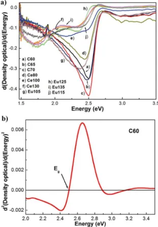
different synthesis times and doping was calculated from optical transmittance data. Fig. 6a shows the first derivative of the optical density [d(OD)/dE] as a function of the incident
photon energy (E) of typical samples. The relative minima
in the transmittance spectra of the first derivative d(OD)/ dE versus E graph define the critical points of the band
structure35,36, which are associated absorption bands due
impurities and vacancies23, as is observed in Fig. 6a. Fig. 6b
illustrates the second derivative of OD plotted against E of
typical samples. A more precise position of the critical point
Eg in the E-axis is defined by the maximum of the second
derivative curve. The estimated optical band gap of the CdS nanofilm is of 2.50 eV that corresponds to pure CdS and is 82 meV higher that band gap in CdS bulk, which indicates that there is quantum confinement. This discrepancy is associated to the average grain size37,38. As is observed in
Fig. 6b band gap energy redshifts slightly with the V[RE3+]
increase or that is the same with the increase of the synthesis time, these results are shown in Fig. 7. The transmittance
spectrum of RE3+-doped CdS is fundamentally similar to that
of single CdS as can see in Fig. 5, with some slight shifts in the absorption band, which are caused by the incorporation of RE in Cd sub-lattice. The main absorption band slightly
redshifts as V[RE3+] increases. The slight reduction of the
main absorption edge is indicative of the compensation of broken bonds, but also it indicates that the RE atoms are being incorporated into interstitials of the unit cell, see Table 1. In order to the Ce135 sample the optical band gap decreased slightly by about 84.22 meV compared with the band gap energy of the C60 sample, which can be related
to RE3+ incorporation to the molecule and the average grain
size. This band gap decrease can be explained due to the
substitution in the sub-lattice of cadmium atoms (ionic radii
~0.95 Å) by cerium (ionic radii 1.15 Å) and europium (ionic radii 1.09 Å) atoms that are larger.
Figure 5. Transmittance spectra of CdS samples synthesized at
different synthesis time
Figure 8 shows the photoluminescence spectra of the single CdS for the four different synthesis times. The energy of the radiative transitions and the linewidth at half-maximum (FWHM) of each band have been determined by a quantitative fit to the experimental PL spectra using a sum of Gaussian line distributions, the dominant peaks were first fit and the additional peaks were added as were necessary. For sample C65, which presents best luminescence, the radiative bands are observed at 434 nm (2.86 eV) (violet), 523 nm (2.37 eV) (green), 565 nm (2.19 eV) (orange), 659 nm (1.88 eV) (red) and 898.21 nm (1.38 eV) (infrared) eV that are labelled by A, B, C, D and E in the PL spectrum of the C65 sample. The band A is associated a radiative transition band-to-band, which is higher than the single CdS band gap for 358 meV. This is due to the quantum confinement associated with grain size since it is less than the exciton Bohr radius. The band B is clearly identified on as-grown CBD-CdS at 523 nm (2.37 eV), which is called the optical signature of interstitial oxygen39.
eV), this band named the "orange band" has been observed between 610 to 596 nm (2.03-2.08 eV)41,42, it is possibly
associated to a donor-acceptor pair (DAP) radiative transition between a donor level related to interstitial cadmium (Icd2+) and an unidentified acceptor level. The ionization energy of this donor has estimated to be between 120 and 206 meV, which corresponds to ICd2+39. Finally, the broad and weak
peak observed in 892 nm (1.39 eV), which disappears when synthesis time increases, it is in the infrared region and is associated with unidentified deep impurities. In the inset of Fig. 8 shows the behaviour of the intensities the four main
bands, clearly is observed that the band C is dominant for
65 min and very weak for other times.
Figure 7. It shows band gap energy as a function of synthesis time
for three sample series
Figure 8. It shows the photoluminescence spectra CdS for three
synthesis times, in which is presented the PL deconvolution of the C65. In inset is shown of the intensity of four the main radiative
transition as function of synthesis time
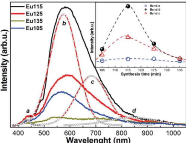
In Fig. 9 the photoluminescence spectra of the Eu3+
-doped CdS samples are shown. It is clearly observed that in the PL spectra the band called the optical signature of interstitial oxygen at ~523 nm (2.37 eV) is not present, which is indicative that the incorporation of rare earths
in CdS lattice decreases the concentration of interstitial
oxygen. The luminescence spectrum of the Eu115 sample, which presents the best luminescence, exhibits four main radiative transitions at 431 nm (2.88 eV), 576 nm (2.15 eV), 683 (1.81 eV) and 840 (1.48) nm (eV). The violet emission peak a at 431 nm is clearly observed, which is associated to
radiative transition band-to-band. This band has been related
to the radiative transition of CdS nanostructures into
band-edge and surface defects due to the quantum confinement effect because of grain size is lower than the exciton Bohr radius, which is greater by 409 meV than its band gap. The dominant radiative peak b at 576 nm (2.15 eV), which has
been associated to the intra-4f radiative transitions of Eu3+
ions that corresponds to the magnetic dipole transition
(5D 0 →
7F1), which was blue shifted compared to previous
Figure 6. a) It is shown the first derivative of the optical absorption
(OD) as a function of the photon energy (hν), for three different
synthesis time values. b) Figure displays the second derivative of
OD versus E, which allows calculate the band gap energy. The
arrows indicate the position of band gap energy, Eg
a band at 563 nm (2.2 eV)39. In addition, the band C could
be attributed to the CdO complexes that would be formed during the growth due to the presence of oxygen during the nucleation of the layer, since the CdO band gap is about 574 nm (2.16 eV)40. For three studied CBD-CdS samples,
results39,43. In Eu3+-doped CdS, the 5D 0 →
7F
1 transition is
mainly magnetically allowed (magnetic-dipole transition). The surface-defect radiative transitions are caused by surface states, such as sulphur vacancies and/or sulphur dangling bonds created by doping are in the wavelength range from 700-500 nm (1.77-2.48 eV)32. Therefore, the peak c at 683
nm (1.81 eV) is associated with surface defects of the CdS nanocrystals. Additionally, the peak d at 840 nm (1.48 eV)
is region of low energies, for which is associated at deep residual impurities. These observations indicate that a part
of Eu3+ ions, contained in CdS nanocrystals and the energy
can be significantly transferred from the host CdS to Eu3+
ions44,45. Upon excitation, the energy from non-radiative recombination of electron-hole pairs can be transferred to the
high energy levels of the Eu ions46,47. The mechanism of the
intensification of (rare earth emission) REE has already been
reported47, which also supports the observed results of the
present study. These results indicate that the adsorbed CdS particles significantly influence the excitation of 4f electrons in rare-earth ion. A significant change in the intensity of the emission bands was observed for the samples prepared using different synthesis time, which are due to the variation in the structures. As is seen in the inset of Fig. 9, peak b is the one
that increases its intensity with the synthesis time, reaching a maximum of 115 min and then decreasing. It may also be attributed to the change in the energy transfer rate with particle size variation and the shape of the nanocrystals.
Figure 9. It presents the photoluminescence spectra of Eu-doped
CdS. In addition, it is shown the deconvolution of dominant PL spectrum, Eu115 sample. In the inset is illustrated the radiative transition bands of the PL spectra as function of the synthesis time
432 nm corresponds to the band-band transition. The band β at 602 nm is the dominant band of PL spectrum, which
is associated to Ce3+ incorporated to the sub-lattice of Cd.
Therefore, it is considered that the radiative transitions present
in the luminescence of the Ce3+-doped CdS have the same
origin as those present in the PL of the Eu3+-doped CdS and
their redshift is due to the ionic radius of the Ce3+ is higher
than the Cd, which strains the lattice.
Figure 10. It illustrates the photoluminescence spectra Ce-doped CdS
for three synthesis times, in which is presented the PL deconvolution of the Ce100 sample. In inset is shown the intensity of four the main
radiative transition as function of synthesis time
Figure 11. Comparison of the best spectra of luminescence, as is
observed the luminescence of the doped samples are shifted to red. The inset illustrates the energy of the photoluminescence intensity maxima as a function of the synthesis time, where the arrows show the samples with the higher luminescent intensity
Figure 10 shows the photoluminescence spectra of the
Ce3+-doped CdS, which are very similar to those obtained
with the Eu3+-doped CdS. The photoluminescence spectrum
of the sample Ce100, which presents the best luminescence, shows radiative bands at 432 nm (2.87 eV), 602 nm (2.06 eV), 726 nm (1.71 eV) and 875 (1.42 eV). The band α at
Figure 11 shows the comparison of the photoluminescence spectra of the three CdS samples with the best results of photoluminescence, single and doped with the rare earths. It is clearly observed that the intensity of the PL spectra of doped CdS increases considerably, indicating that there is a
passivation of the surface state density of the nanocrystals,
4. Conclusions
(Eu,Ce)-doped CdS nanostructures were synthesised by chemical bath deposition technique. Synthesised samples showed cubic zinc-blende crystalline phase of CdS, which was obtained by powder XRD and HRTEM analyses. The incorporation of rare earths in the CdS lattice was confirmed by X-ray diffraction. Transmittance spectra reveal the blueshift of absorption edge by incorporation of rare earths, which allowed estimate the band gaps of RE3+-doped CdS,
which confirms the quantisation effect by grain size in the synthesized samples. It was observed that the structure, crystallite size and the band gap of the europium and cerium doped CdS nanocrystals can be finely controlled by simply varying the synthesis time. The room temperature
photoluminescence of the undoped CdS presents the band-band transition associated to CdS nanocrystals and the
transitions associated with residual impurities and structural defects, mainly the optical signature of interstitial oxygen. The samples doped with rare earths present the band-band
transition, in addition the radiative band associated to the
intra-4f radiative transitions of Eu3+ ions that corresponds
to the magnetic dipole transition (5D 0 →
7F1). For the case of
cerium-doped samples, the results obtained were similar to those for europium. The results confirm that at least a part of
the Eu3+ ions is effectively doped into CdS nanocrystals and
the energy transfer occurs from CdS nanocrystals to Eu3+ ions.
5. Acknowledgments
The authors also thank the SIP-IPN. One of the authors wishes to thank CONACYT for the doctorate scholarship. Another of the authors wishes to thank the Department of Physics, the Postgraduate in Nanotechnology of the University of Sonora and the CONACYT programs that strengthen the scientific and human effort of the authors. The authors would like to thank Ms. Janeth Flores-Martínez for her technical support and as well as valuable discussions that made this research possible.
6. References
1. Stouwdam JW, Hebbink GA, Huskens J, van Veggel FCJM. Lanthanide-Doped Nanoparticles with Excellent Luminescent Properties in Organic Media. Chemistry of Materials.
2003;15(24):4604-4616.
2. Blasse G, Grabmaier BC. Luminescent Materials. Berlin
Heidelberg: Springer Verlag; 1994.
3. Digonnet MJF. Rare-Earth-Doped Fiber Lasers and Amplifiers,
Revised and Expanded. Boca Raton: CRC Press; 2001.
4. Reisfeld R, Jørgensen CK. Lasers and Excited States of Rare
Earths. Berlin Heidelberg: Springer Verlag; 1977.
5. Konishi M, Isobe T, Senna M. Enhancement of photoluminescence of ZnS: Mn nanocrystals by hybridizing with polymerized acrylic acid. Journal of Luminescence. 2001;93(1):1-8.
6. Chowdhuri A, Gupta V, Sreenivas K, Kumar R, Mozumdar S, Patanjali PK. Response speed of SnO2-based H2S gas sensors with
CuO nanoparticles. Applied Physics Letters.
2004;84(7):1180-1182.
7. Yang P, Liou KN, Mishchenko MI, Gao BC. Efficient finite-difference time-domain scheme for light scattering by dielectric particles: application to aerosols. Applied Optics.
2000;39(21):3727-3737.
8. Simon DT, Geller MR. Electron-phonon dynamics in an ensemble of nearly isolated nanoparticles. Physical Review B. 2001;64(11):115412.
9. Jayaraj MK, Vallabhan CPG. AC Thin Film Electroluminescent Devices with Rare Earth Doped ZnS. Journal of the Electrochemical
Society. 1991;138(5):1512-1516.
10. Jing L, Sun X, Xin B, Wang B, Cai W, Fu H. The preparation and characterization of La doped TiO2 nanoparticles and their
photocatalytic activity. Journal of Solid State Chemistry.
2004;177(2004):3375-3382.
11. Vij A, Singh S, Kumar R, Lochab SP, Kumar VVS, Singh N. Synthesis and luminescence studies of Ce doped SrS nanostructures.
Journal of Physics D: Applied Physics. 2009;42(10):105103.
12. Kumar V, Mishra V, Pitale SS, Nagpure IM, Coetsee E, Ntwaeaborwa OM, et al. Surface chemical reactions during
electron beam irradiation of nanocrystalline CaS:Ce3+ phosphor.
Journal of Applied Physics. 2010;107(12):123533.
13. Switzer JA, Hodes G. Electrodeposition and chemical bath deposition of functional nanomaterials. MRS Bulletin.
2010;35(10):743-750.
14. Kozhevnikova NS, Vorokh AS, Uritskaya AA. Cadmium sulfide nanoparticles prepared by chemical bath deposition. Russian
Chemical Reviews. 2015;84(3):225-250.
15. Hodes G. Chemical Solution Deposition of Semiconductor
Films. New York: Marcel Dekker; 2003.
16. Kaur I, Pandya DK, Chopra KL. Growth Kinetics and Polymorphism of Chemically Deposited CdS Films. Journal
of the Electrochemical Society. 1980;127(4):943-948.
17. Froment M, Lincot D. Phase formation processes in solution at the atomic level: metal chalcogenide semiconductors.
Electrochimica Acta. 1995;40(10):1293-1303.
18. O'Brien P, McAleese J. Developing an understanding of the processes controlling the chemical bath deposition of ZnS and CdS. Journal of Materials Chemistry. 1998;8(11):2309-2314.
19. Nakada T, Mizutani M. 18% efficiency Cd-free Cu(In, Ga)Se2 thin-film solar cells fabricated using chemical bath deposition (CBD)-ZnS buffer layers. Japanese Journal of Applied Physics.
2002;41(Pt 2 2B):L165-L167.
20. Liu QQ, Shi JH, Li ZQ, Zhang DW, Li XD, Sun Z, et al. Morphological and stoichiometric study of chemical bath deposited CdS films by varying ammonia concentration. Physica
B: Condensed Matter. 2010;405(20):4360-4365.
21. Radhu S, Vijayan C. Observation of red emission in wurtzite ZnS nanoparticles and the investigation of phonon modes by Raman spectroscopy. Materials Chemistry and Physics.
22. Peng WQ, Cong GW, Qu SC, Wang ZG. Synthesis of shuttle-like ZnO nanostructures from precursor ZnS nanoparticles.
Nanotechnology. 2005;16(9):1469-1473.
23. Díaz-Reyes J, Contreras-Rascón JI, Galván-Arellano M, Arias-Cerón JS, Gutiérrez-Arias JEM, Flores-Mena JE, et al. Physical Property Characterization of Pb2+-Doped CdS Nanofilms Deposited by Chemical-Bath Deposition at Low Temperature.
Brazilian Journal of Physics. 2016;46(6):612-620.
24. Singh J. Physics of Semiconductors and Their Heterostructures.
New York: McGraw-Hill; 1993.
25. Yamaguchi K, Yoshida T, Sugiura T, Minoura H. A Novel Approach for CdS Thin-Film Deposition: Electrochemically Induced Atom-by-Atom Growth of CdS Thin Films from Acidic Chemical Bath. Journal of Physical Chemistry B.
1998;102(48):9677-9686.
26. Ziabari AA, Ghodsi FE. Influence of Cu doping and
post-heat treatment on the microstructure, optical properties and
photoluminescence features of sol-gel derived nanostructured CdS thin films. Journal of Luminescence. 2013;141:121-129.
27. Murugadoss G. Synthesis of high quality and monodisperse CdS:Mn2+/ZnS and CdS:Mn2+/CdS core-shell nanoparticles.
Superlattices and Microstructures. 2012;52(5):1026-1042.
28. Guglielmi M, Martucci A, Fick J, Vitrant G. Preparation and Characterization of HgxCd1-xS and PbxCd1-xS Quantum Dots and
Doped Thin Films. Journal of Sol-Gel Science and Technology.
1998;11(3):229-240.
29. J. A. Dean. Handbook of Chemistry. McGraw Hill Book Co.,
Beijing, 1999.
30. N. A. Lange, J. A. Dean. Handbook of Chemistry, 13th Ed. New
York: McGraw-Hill. 1987.
31. Ortega-Borges R, Lincot D. Mechanism of Chemical Bath Deposition of Cadmium Sulfide Thin Films in the Ammonia-Thiourea System. In Situ Kinetic Study and Modelization. Journal
of the Electrochemical Society. 1993;140(12):3464-3473.
32. Grus M, Sikorska A. Characterization of the absorption edge in crystalline CdS:Cu powder by use of photoacoustic and reflection spectroscopy. Physica B: Condensed Matter.
1999;266(3):139-145.
33. Díaz-Reyes J, Contreras-Rascón JI, Arias-Cerón JS, Sánchez-Ramírez JF, Galván-Arellano M, Martínez-Juárez J, et al.
Structural and optical characterisation of CdSe1-ySy. Materials
Science in Semiconductor Processing. 2015;37:199-206.
34. Esmaili M, Habibi-Yangjeh A. Microwave-Assisted Preparation of CdS Nanoparticles in a Halide-Free Ionic Liquid and Their Photocatalytic Activities. Chinese Journal of Catalysis.
2011;32(6-8):933-938.
35. Potter BG Jr., Simmons JH. Quantum-confinement effects in CdTe-glass composite thin films produced using rf magnetron sputtering. Journal of Applied Physics. 1990;68(3):1218-1224.
36. Katsikas L, Eychmüller A, Giersig M, Weller H. Discrete excitonic transitions in quantum-sized CdS particles. Chemical
Physics Letters. 1999;172(3-4):201-204.
37. Seo DJ. Structural and Optical Properties of CdO Films Deposited by Spray Pyrolysis. Journal of the Korean Physical Society.
2004;45(6):1575-1579.
38. Jin BJ, Woo HS, Im S, Bae SH, Lee SY. Relationship between photoluminescence and electrical properties of ZnO thin films grown by pulsed laser deposition. Applied Surface Science.
2001;169-170:521-524.
39. Gemain F, Robin IC, Renet S, Bernardi S. Photoluminescence studies of CdS layers for solar cells. Physica Status Solidi C.
2012;9(8-9):1740-1743.
40. Jefferson PH, Hatfield SA, Veal TD, King PDC, McConville CF, Zúñiga-Pérez J, et al. Bandgap and effective mass of epitaxial cadmium oxide. Applied Physics Letters. 2008;92(2):022101.
41. Mochizuki K, Satoh M, Igaki K. Orange Luminescence in CdS.
Japanese Journal of Applied Physics. 1983;22(Pt 1
9):1414-1417.
42. Abken AE, Halliday DP, Durose K. Photoluminescence study of polycrystalline photovoltaic CdS thin film layers grown by close-spaced sublimation and chemical bath deposition. Journal
of Applied Physics. 2009;105(6):064515.
43. Patra A, Sominska E, Ramesh S, Koltypin Y, Zhong Z, Minti H, et al. Sonochemical Preparation and Characterization of Eu2O3 and
Tb2O3 Doped in and Coated on Silica and Alumina Nanoparticles.
Journal of Physical Chemistry B. 1999;103(17):3361-3365.
44. Hayakawa T, Selvan ST, Nogami M. Field enhancement effect of small Ag particles on the fluorescence from Eu3+-doped SiO
2
glass. Applied Physics Letters. 1999;74(11):1513-1515.
45. Singh K, Kumar S, Verma NK, Bhatti HS. Photoluminescence
properties of Eu3+-doped Cd
1-xZnxS quantum dots. Journal of
Nanoparticle Research. 2009;11(4):1017-1021.
46. Del Castillo J, Rodríguez VD, Yanes AC, Méndez-Ramos J, Torres ME. Luminescent properties of transparent nanostructured
Eu3+-doped SnO
2-SiO2 glass-ceramics prepared by the sol-gel
method. Nanotechnology. 2005;16(5):S300-S303.
47. Reisfeld R, Gaft M, Saridarov T, Panczer G, Zelner M. Nanoparticles of cadmium sulfide with europium and terbium in zirconia films having intensified luminescence. Materials