51
PACS 61.05.cm, 61.46.Hk, 62.20.Qp.68.37.Hk, 81.15.-z
SIMULATION STUDY OF EFFECTS, OPERATING TEMPERATURE AND LAYER THICKNESS ON THIN FILM CIGS SOLAR CELL
PERFORMANCE
A.D. Pogrebnjak, A.K.M. Muhammed
Sumy State University,
2, Rimsky-Korsakov Str., 40007 Sumy, Ukraine E-mail: [email protected]
SCAPS- program is designed basically for the simulation and studying the properties of photonic devices. We explored the important controllable design parameters affecting the performance of the hetero junction solar cells, as operating temperature that we noticed increasing in J-V characteristics by increasing T. The effect of thickness of each layer on the performance of the cell was studied, an increasing of J-V characteristics with increasing p-layer. In the numerical example, 3 m absorber layer and CdS layer 0.05 m, ZnO layer 0.1 m, works the best for given doping density, if we change the optimum value, the efficiency can reach to 17.72 % with FF 83.88 %, Voc 0.725 Volt, Jsc 29.07 mA/cm2 at 300 K, in this case, we have come out the optimum parameters to achieve the best performance of this type of cell, and then to made comparison with practical CIGS cell.
Keywords: CIGS, SCAPS, SOLAR CELL, HETERO-JUNCTION, OPERATING TEMPERATURE, THICKNESS.
(Received 21 September 2011, in final form 27 October 2011 published online 05 November 2011)
1. INTRODUCTION
Simulation of thin film solar cells has become increasingly mature and complex over the last two decades. A number of simulation packages have been developed at universities or research institutes , and use atypically available at no cost and without support .This group of programs includes AMPS-ID, SCAPS-ID, PC-ID, ASA, and AFORS-HET [1]. Among these programs is SCAPS-ID that used in this work, SCAPS-ID, an acronym for
function of the buffer layer is to be a good hetero-junction partner to the p-type absorber layer with minimal lattice mismatch to minimize defects like interface states and be transparent to incident light [5]. The window layers transmit most of the light from the solar spectrum owing to their large band gaps, for the n-type partner in the junction , which at the same time needs to be sufficiently conductive to serve as front contact, ZnO is a cheap and rather easy to grow, making it the general choice [7].
2. SIMULATION RESULTS
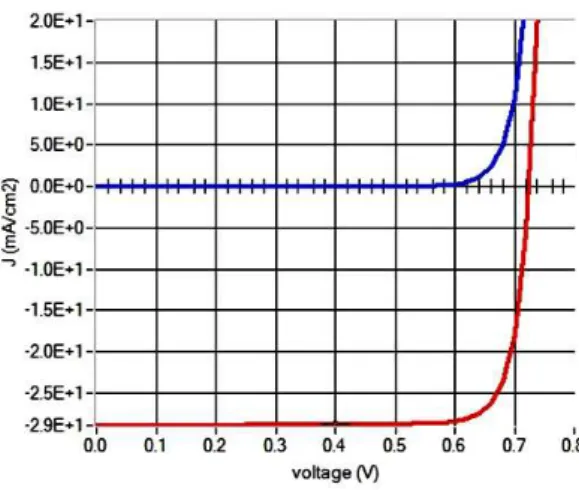
Modeling result of the CIGS solar cell that shown in Fig. 1 is the light –
dark J-V plots (Voc 725 mV, Jsc 28.9 mA/cm2, FF 84.14, 17.65%).
Fig. 1 – Light/Dark J-V curves of CIGS solar cell
Quantum efficiency shown in Fig. 2 shows a peak response of (I-R) % (70-80) and falls off in the range below (300 – 400) nm due to the recombination and absorption in the CdS and ZnO.
3. EFFECT OF THE OPERATING TEMPERATURE
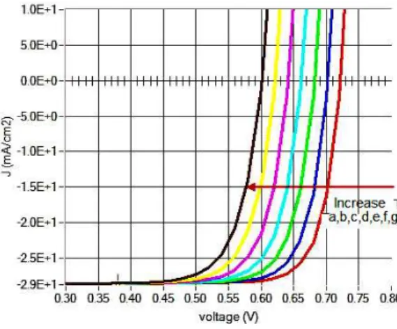
Operating temperature plays a vital role in the performance of solar cells. The optimum operating temperature that has been used for most of the simulation in this study is 300 K or 27 oC .In a solar cell, the parameter most affected by an increase in temperatures is the open circuit voltage (Voc).The impact of increasing temperature on Voc is shown in Fig. 3. Fig. 3 illustrate Voc decrease with temperature because of the temperature
dependence of the reverse saturation current (Is).
Fig. 3 – I-V parameters CIGS solar cell at various temperatures, a-300, b-310, c-320, d-330, e-40, f-350, g-360 K
Many of the parameters of Is have some temperature dependence, but the most significant effect is due to the intrinsic carrier concentration (ni) The band gap energy has been slightly narrowed and this may accelerate the recombination of electron-hole pairs (EHP) between valance band and conduction band, but the band gap energy at higher temperature is unstable which may lead to recombination of electrons and holes while traveling across the regions. So that Jsc is slightly decreased as shown in Table 1. The dependence of the fill factor (FF %) on the operating temperature can be
Table 1 – J-V parameters CIGS solar cell at various temperatures
, % FF, %
Jsc, (mA)
Voc, (Volt)
T, (K)
17.42 83.88
28.742 0.722
300
16.79 83.22
28.738 0.702
310
16.18 82.54
28.736 0.682
320
15.58 81.84
28.734 0.660
330
14.96 81.08
28.732 0.640
340
14.34 80.30
28.730 0.620
350
13.72 79.50
28.728 0.600
deviated from the dependence of the Voc on the temperature. FF % inversely
proportional with the operating temperature as shown in Table 1.The reduction in the Voc and Jsc and FF % with the temperature leads to reduction in the efficiency ( %) with the temperature.
4. EFFECT OF CIGS ABSORBER LAYER THICKNESS
The effect of the CIGS absorber thickness on Voc and Jsc is shown in Table 2. Both values increased when the thickness of CIGS absorber layer increased wavelengths of the illumination to be absorbed, which in turn contribute in EHP generation. The long wavelength photons will be deeper with in the CIGS layer, so that the FF %, and % increased with increases CIGS thickness as shown in Table 2, and we illustrate the best value of the efficiency at the thickness 3 m of CIGS solar cell and equal to 17.72.
Table 2 – J-V parameters CIGS solar cell at various absorber layer thickness
% FF %
Jsc, mA/cm2
Voc, (Volt)
CIGS, Thickness, m
14.90 81.39
27.03 0.677
0.3
15.95 82.26
27.90 0.694
0.8
16.58 83.01
28.30 0.705
1.3
17.03 83.47
28.61 0.712
1.8
17.37 83.72
28.84 0.719
2.3
17.63 83.96
29.01 0.723
2.8
17.72 84.04
29.07 0.725
3
So that the effect of CIGS absorber layer on the quantum efficiency has been occurred in the region extended from ( 400-1200nm) as shown in Fig. 4,
for thin absorber the generation region will be near the high recombination back contact region, this will reduces the number of the generated electron –
hole pairs and the quantum efficiency. For thick absorber cell, the generation process has been occurred far from the back contact region so that the quantum efficiency will increased.
5. EFFECT OF CdS BUFFER LAYER THICKNESS
Generally, the thickness of the optimum CdS buffer layer should be within 50 nm – 60 nm. In this study the thickness of CdS has been varied from (0.001) to (0.1) μm, Voc and Jsc will be decreased when the thickness of CdS layer increased as Table 3.
Table 3 – J-V parameters CIGS solar cell at various CdS layer thickness
, % FF %
Jsc, mA/cm2
Voc, (Volt )
CdS, Thickness, m 17.66 84.08 28.955 0.7522 0.001 17.65 84.07 28.946 0.7522 0.005 17.64 84.06 28.916 0.7521 0.025 17.63 84.06 28.894 0.7521 0.05 17.62 84.05 28.890 0.7520 0.06 17.61 84.05 29.888 0.7519 0.08 17.60 84.04 29.886 0.7518 0.1
This because a thicker buffer layer will result in higher photon absorption as loss. FF% also decreased due to the reduction in Voc and Jsc as shown in
Table 1. When the buffer layer increases, more photons which carry the energy (h Eg CdS) are being absorbed by this layer, therefore it will be lead to decrease in the number of photons which could reach the absorber layer as a result the efficiency has been decrease from (17.66) to (17.60) as shown Table 1, and we found that the thickness of CdS of 10 nm give the highest efficiency (17.66).
6. EFFECT OF ZNO WINDOW LAYER THICKNESS
The effect of ZnO thickness on the output parameter of CIGS cell has been fo-und to be the similar to the effect of CdS layer but is defer in magnitude. An increase in the thickness of ZnO layer will decrease in Voc, Jsc as shown in
Table 4.
Table 4 – J-V parameters CIGS solar cell at various ZnO layer thickness
% FF %
Jsc,mA/cm2 Voc, (Volt)
ZnO, Thickness, m
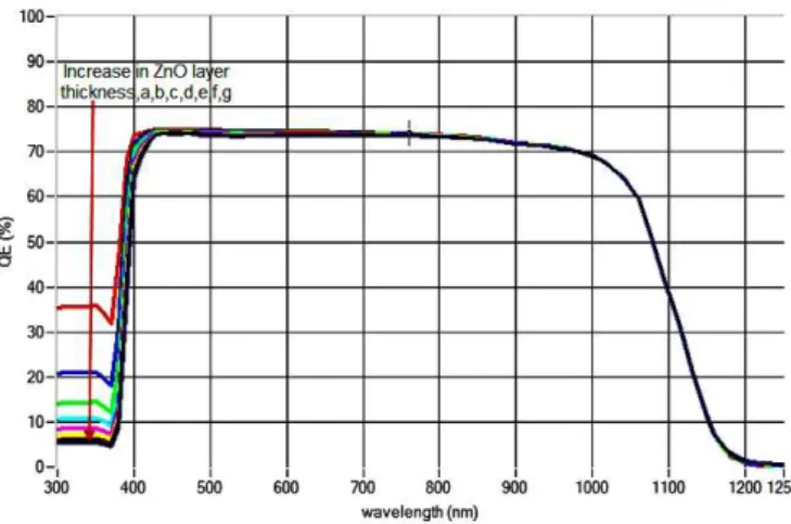
FF % decreased from (84.1) to (84.03) as shown in Table 4, the efficiency decreased from (17.82) to (17.44). This effect will also appear as a loss in the quantum efficiency in region ( 300-400 nm) as shown in Fig. 5.
Fig.5 – Quantum efficiency of CIGS solar cell at various ZnO layer thickness a-0.05, b-0.07, c-0.1, d-0.2, e-0.3, f-0.4, g-0.5 m
7. PRACTICAL RESULTS
To compare our simulation results with the practical results obtained by (7), that used thickness of layers, absorber layer equal 2 m, CdS layer 0.02 m and ZnO layer equal 0.5 m, the results for comparison shown in Table 5.
Table 5 – Output practical and simulation result for CIGS solar cell
% FF %
Jsc, mA/cm2 Voc, Volt
Type
12 68
40 0.475
Practical result
16.94 83.64
28.307 0.715
Simulation result
The difference between the simulation and the practical study was due to interface state and surface recombination included in real device. The parameter from the simulation study is listed in Table 7.
8. CONCLUSION
ИМИТАЦИОННОЕ МОДЕЛИРОВАНИЕ ВЛИЯНИЯ РАБОЧЕЙ ТЕМПЕРАТУРЫ И ТОЛЩИНЫ СЛОЯ НА ХАРАКТЕРИСТИКИ ТОНКОПЛЕНОЧНОГО
СОЛНЕЧНОГО ЭЛЕМЕНТА CIGS
А.Д.По ребняк, A.K.M. Мухамме
Сумский осу арственный университет
ул. Римско о-Корсакова, 2, 40002 Сумы, Украина
E-mail: [email protected]
Про рамма SCAPS разработана с ел мо елирования и изу ения свойств фотонных приборов. Были иссле ованы важные ре улируемые конструктивные
параметры, влия щие на характеристики солне ных элементов с
етероперехо ом, в астности, рабо ая температура. Было заме ено, то вол т
-амперные характеристики (ВАХ) возраста т с увели ением температуры T. В иссле овании было изу ено влияние толщины каж о о слоя на свойства солне но о элемента. Также было опре елено, то ВАХ возраста т с увели ением
p-слоя. На исленном примере, слой по лощения 3мкм и CdS слой 0,05мкм, ZnO слой 0,1мкм явля тся наилу ими параметрами ля за анной кон ентра ии примеси. Если изменит оптимал ное зна ение, то эффективност может ости ат 17,72з с FF 83,88 %, Voc 0,725В, Jsc 29,07мA/см2 при 300 К. В
этом слу ае можно полу ит оптимал ные параметры ля остижения
наилу их характеристик это о типа фотоэлементов и затем сравнит с характеристиками элементов CIGS (ме -ин ий- иселени аллия).
Ключевые слова: CIGS, SCAPS, СОЛНЕЧНЫЙ ЭЛЕМЕНТ, ГЕТЕРОПЕРЕХОД,
РАБОЧАи ТЕМПЕРАТУРА, ТОЛЩИНА.
ІМІТАЦІЙНЕ МОДЕЛЮВАННЯ ВПЛИВУ РОБОЧОЇ ТЕМПЕРАТУРИ І ТОВЩИНИ ШАРУ НА ВЛАСТИВОСТІ ТОНКОПЛІВКОВОГО СОНЯЧНОГО
ЕЛЕМЕНТУ CIGS
А.Д.По ребняк, A.K.M. Мухамме
Сумський ержавний університет
вул. Римсько о-Корсакова, 2, 40002 Суми, Україна
E-mail: [email protected]
Про рама SCAPS розроблена з мето мо ел вання і вив ення властивостей фотонних прила ів. Були ослі жені важливі ре ул овані конструктивні параметри, що вплива т на характеристики соня них елементів з етероперехо ом, зокрема, робо а температура. Було ві мі ено, що вол т
-амперні характеристики (ВАХ) зроста т зі збіл енням температуриT. У ослі женні вив ено вплив товщини кожно о ару на властивості соня но о елементу. Також було визна ено, що ВАХ зроста т зі збіл енням p- ару. На исел ному прикла і, ар по линання 3мкм і CdS ар 0.05мкм, ZnO ар
0.1мкм, є найкращими параметрами ля за аної кон ентра ії омі ки. икщо змінити оптимал не зна ення, то ефективніст може ося ати 17,72з з
FF 83,88 %, Voc 0,725В, Jsc 29,07мА/см2 при 300К. В ому випа ку
можна отримати оптимал ні параметри ля ося нення найкращих
характеристик о о типа фотоелементів і порівняти з характеристиками елементів CIGS (мі -ін ій- иселені алі ).
Ключові слова: CIGS, SCAPS, СОНиЧНИЙ ЕЛЕМЕНТ, ГЕТЕРОПЕРЕХІД,
REFERENCE
1. M. Burgelman, J. Verschaegen, S. Degrave, P. Nellet, Modeling thin film PV de-vices, progress in photovoltaic: Research and Application (John Wiley & sons: 2004). 2. M. Burgelman, J. Verschaegen, S. Degrave, P. Nellet, Modeling Polycrystalline
Semiconductor Solar Cell, Thin Solid Films, (Elsevier: 2000).
3. M. Burgelman, SCAPS User Manual, (ELIS-Univercity of Gent: 2007).
4. J.A.M. Abushama, S. Johanston, T. Moriarty, G. Teeter, K. Ramanathan, R. Noufi, Prog. Photovolt: Ress. Appl. 12, 39 (2004).
5. B. Dimmler, M. Powalla, H.W. Schoch, Prog. Photovolt: Ress. App. 10, 149 (2002). 6. J. Lahnemann, Spectrally resolved current losses in Cu (In, Ga)Se2 Thin Film
Solar Cells, (Diploma thesis: freie Univesitat Berlin: 2008).