*e-mail: [email protected]
Photoluminescence Properties of Thermally Stable Highly Crystalline CdS Nanoparticles
Sanjay R. Dhagea*, Henry A. Coloradob,c, Hong Thomas Hahna,b
aMechanical and Aerospace Engineering Department, University of California,
Los Angeles, CA 90095, USA
bMaterials Science and Engineering Department, University of California, Los Angeles, CA 90095, USA cUniversidad de Antioquia, Mechanical Engineering. Medellin-Colombia
Received: July 24, 2012; Revised: October 15, 2012
Thermally stable and highly crystalline CdS nanoparticles were obtained via chemical bath method. The optical properties of CdS nanocrystals were characterized by ultraviolet-vis and photoluminescence spectroscopy. Improvement in the photoluminescence properties of the synthesized CdS nanocrystals was observed. This improvement is believed to be due to highly crystalline CdS nanoparticles which may reduce the local surface-trap states. The CdS nanoparticles were characterized by x-ray powder diffraction (XRD), thermo gravimetric analysis (TGA/DTA) and transmission electron microscopy (TEM).
Keywords: CdS, chemical synthesis, x-ray diffraction, TEM, optical properties
1. Introduction
CdS is a II-VI semiconductor with a direct band-gap of about 2.4 eV. It has a wide range of applications including phosphors and photovoltaic cells. The potential application of CdS film deposited by chemical bath involves photovoltaics and most of uses of nanocrystals, e.g. in photonics or recently in quantum computing1.
Over the past few years, various new routes have been developed to synthesize CdS nanostructures including template assisted synthesis2, colloidal micelle3, solvothermal method4, a method based on nitrilotriacetic acid (N(CH2COOH)3) as complex5 of Cd, carboxyl, and amine terminated PAMAM dendrimers stabilizing agents6. All of the above mentioned methods include various complexing and stabilizing agents.
Research efforts7 devoted to chemical bath deposition (CBD) of CdS thin films are motivated by the need for improvement of window layers in the solar cells based on CdTe and Cu(In,Ga)Se2. In particular, CBD is widely used for achieving good-quality CdS8-10. In recent years, a larger number of techniques have been developed to permit the control of synthesis of CdS nanocrystals, as well as the size, morphology, thermal stability and luminescence properties; however, success is limited.
In the present study we investigate thermally stable highly crystalline CdS nanoparticles synthesized by chemical bath with improved photoluminescence properties. The obtained CdS nanocrystals were characterized by XRD, TGA/DTA, TEM, UV-Vis and photoluminescence spectroscopy.
2. Experimental Procedure
CdSO4 and thiourea were used as Cd and S ions source respectively, and ammonia was used as a complexing agent for Cd ions. All the used chemicals were used of AR grade without further purification purchased from Aldrich chemicals. The synthetic method for CdS nanoparticles used in this work was based on a previously reported procedure11. The CdSO
4 (0.16 M) solution was first added to NH3 (7.5 M) solution under stirring followed by addition of thiourea (0.6 M) solution. The bath temperature and pH was maintained at about 65 °C and 10 respectively, with constant stirring. Precipitated yellow solid product was centrifuged and dried in the oven at 65 °C overnight. The particles were then annealed in the furnace at different temperatures to examine the thermal stability. The chemical reactions involved in the formation of CdS are described below. CdSO4 + nNH3→ [Cd(NH3)n]2+ + SO
42– (1)
[Cd(NH3)n]2+→ Cd2+ + nNH
3 (2)
SC(NH2)2 + 2OH–→ S2– + CN
2H2 + 2H2O (3)
Cd2+ + S2–→ CdS (4)
The crystal phase analysis of the synthesized nanoparticles was determined by an x-ray powder diffractometer (XRD, Cu Kα radiation) (Phillips) with a Bragg angle ranging from 20 to 60°. TGA/DTA was recorded to study the thermal stability and phase transformation of the prepared CdS nanoparticles. Transmission Electron Microscopy (TEM) (JEOL, 100CX) and Selected Area Electron Diffraction (SAED) patterns were obtained to examine the particle size, OI:
D 10.1590/S1516-14392013005000020
Photoluminescence Properties of Thermally Stable Highly Crystalline CdS Nanoparticles
morphology and diffraction patterns of the crystalline CdS nanoparticles. The optical absorption of CdS nanoparticles was examined by a perkin-Elmer lamda20 UV/Visible spectrometer. The photoluminescence spectrum was achieved on a PTI fluorescence spectrometer.
3. Results and Discussion
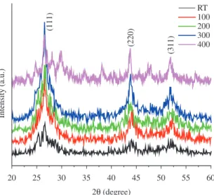
Figure 1 shows the XRD patterns of the CdS nanoparticles oven dried at 65 °C and annealed at various temperatures. The XRD of the oven dried particles shows all the planar reflections (111), (220) and (311) corresponding to the cubic crystal structure of CdS which was in good agreement with the reported reference (JCPDS No. 10-0454). The peak (111) of the cubic structure CdS is similar to the (002) peak of the hexagonal structure CdS. However, the other peaks of the hexagonal CdS do not appear. Thus, it is more likely that the structure is predominantly cubic, similarly to the other report12-15. No other impurities could be detected indicating the high quality of the sample. The XRDs of samples at 100, 200 and 300 °C show the same pattern as the oven dried particles. In addition, thermal annealing effect is shown in the narrowing of the dominant peaks, indicating an increase of the nanocrystals’ size, which clearly indicates that the crystalline particles are thermally stable up to 300 °C. However the XRD of 400 °C shows impurity peaks along with the cubic CdS phase. Therefore the collapse of the cubic crystalline structure or the generation of impurity phases begin at about 400 °C; A resultant observation that is supported by TGA/DTA data. Figure 2 shows the TGA/DTA of the as prepared CdS nanoparticles. Weight loss at about 200 °C corresponds to the adsorbed water on the surface of nanocrystals. The broad exotherm that starts at about 400 °C is supporting evidence for the collapse of cubic crystal structure of CdS and evolution of various impurity phases. The TGA/DTA result was in good agreement with the XRD.
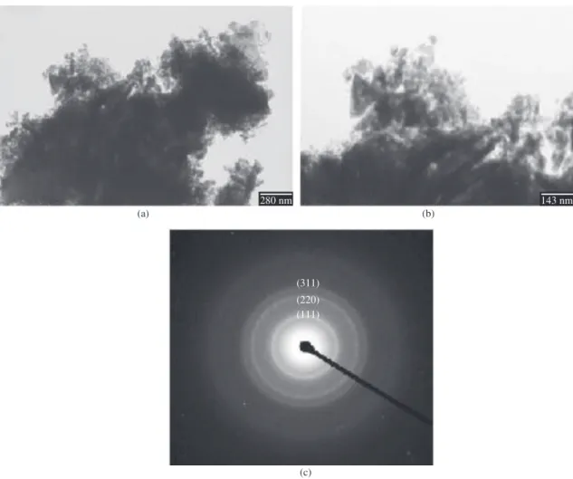
Figure 3a, b shows the overall TEM image of the prepared oven dried CdS particles. The typical morphology of the CdS is small spheres with an average diameter of about 10 nm; however, some irregularly shaped particles were also observed. The agglomeration of particles in TEM may have arisen from the small dimensions and high surface energy. The selected area diffraction (SAED) pattern shows the multicrystal structure of the CdS nanoparticles as shown in Figure 3c. The diffraction rings correspond to cubic CdS crystal structure. The presence of a very intense ring corresponding to d value of 3.36 Å confirms that the films are composed of highly crytalline CdS of cubic phase. Planer reflection of (111), (220) and (311) can be seen in the SAED pattern of the CdS nanocrystals which agreed well with the XRD pattern.
The powder CdS nanoparticles were dispersed into DI water using ultrasonic bath. Then the UV-Vis and photoluminescence spectra of the CdS colloidal solution were recorded. Figure 4 shows the photoluminescence spectra of the prepared CdS nanoparticles. The typical UV-Vis absorption spectra of the CdS; nanoparticle recorded at room temperature is shown in the inset of Figure 4. The absorption peak at 480 nm belongs to CdS, it can be also observed that there are tails of more intense absorption occurring at shorter wavelengths which are due to higher
energy electronic transitions as observable in low band gap semiconductor nanoparticles13. It was found that the CdS nanoparticle colloidal solution exhibited a PL peak centered at 449.7 nm. Because of the high surface-to-volume ratio, the PL efficiency of nanocrystals can be dramatically reduced by localized surface-trap states16-19. The CdS nanocrystals in the present study reduce effectively the local surface-trap states because of the highly crystalline nature of nanoparticles and the uniform dispersion of CdS nanocrystals in DI water. Much effort has been spent to study luminescence properties of CdS nanocrystals. It has been reported20 two emission bands, one is the green emission 552 nm, and the other is the broad red emission at 744 nm. Also, it has been found21 there were two luminescence peaks at 680 nm and 760 nm (IR), which were attributed to the formation of the sulfur vacancies (Vs) and Cd–S composite vacancies (Vcd-s), respectively. It has been reported22 that Q-CdS showed the band edge PL peak centered at 450 nm. Also, it has been reported23 that before and after modification of CdS nanocrystals capped by ethylene diamine shows a PL peak centered at 450 nm. In this paper, the CdS nanocrystals Figure 1. XRD of oven dried and annealed CdS nanocrystals at different temperature.
Figure 2. TG/DT analysis of the as prepared oven dried CdS nanocrystals.
Dhage et al.
exhibit a PL peak centered at 449.2 nm. An increase in PL emission intensity many times higher than the reported results was observed. It is suggested that the emission peak at 449.7 nm is attributed to the transition from conduction
band to valance band and the emission peak blue shifts due to the quantum confined effect.
4. Conclusions
Thermally stable highly crystalline CdS nanoparticles were synthesized by chemical bath method. We have demonstrated the thermal stability and phase transformation of the CdS nanocrystals with respect to annealing temperature. The improved photoluminescence properties of the prepared CdS nanocrystals may provide a useful system for studies of the chemical and physical properties of the surface-traps on semiconducting nanoparticles.
Acknowledgements
The present paper is based on work supported by the Air Force Office of Scientific Research through a MURI grant FA9550-06-1-0326 to the University of Washington. We are thankful to the NSF IGERT Materials Creation Training Program (MCTP)-DGE-0654431 for the use of its analytical facilities. Appreciation is extended to Prof. Q. Pei for UV-Vis and PL facility.
Figure 3. a) Overall TEM image, b) image at high resolution and c) selected area diffraction pattern of as prepared CdS nanocrystals.
Figure 4. Photoluminiscence spectra of CdS nanocrystals. For the PL spectra 390 nm wavelength was used for the excitation. Inset: UV-Visible absorption spectra of the CdS nanoparticles at 200-700 nm.
Photoluminescence Properties of Thermally Stable Highly Crystalline CdS Nanoparticles
References
1. DiVincenzo DP. Real and realistic quantum computers. Nature. 1998; 393:113-114. http://dx.doi.org/10.1038/30094 2. Routkevitch D, Bigioni T, Moskovits M and Xu JM.
Electrochemical fabrication of CdS nanowire arrays in porous anodic aluminum oxide templates. The Journal of Physical Chemistry. 1996; 100(33):14037-14047. http://dx.doi. org/10.1021/jp952910m
3. Xiong YJ, Xie Y, Yang J, Zhang R, Wu CZ and Du GA. In situ micelle-template-interface reaction route to CdS nanotubes and nanowires. Journal of Materials Chemistry. 2002; 12:3712-3716. http://dx.doi.org/10.1039/b206377h
4. Gai H, Wu Y, Wang Z, Wu L, Shi Y, Jing M et al. Polymer-assisted solvothermal growth of CdS nanowires. Polymer Bulletin. 200; 61:435-441.
5. Tang H, Yan M, Zhang H, Xia M and Yang D. Ammonia-free chemical bath deposition of CdS films: tailoring the nanocrystal sizes. Journal of Crystal Growth. 2002; 240:484-488. http:// dx.doi.org/10.1016/S0022-0248(02)00930-2
6. Sooklal K, Hanus LH and Ploehn HJ. A Blue-Emitting CdS/Dendrimer Nanocomposite. Advanced
Materials. 1998; 10(14):1083-1087. http://dx.doi.
org/10.1002/(SICI)1521-4095(199810)10:14%3C1083::AID-ADMA1083%3E3.0.CO;2-B
7. Chu TL, Chu SS, Ferekides C, Wu CQ, Britt J and Wang C. 13.4% efficient thin film CdS/CdTe solar cells. Journal of Applied Physics. 1991; 70(12):7608-7612. http://dx.doi. org/10.1063/1.349717
8. Pintilie L, Pentia E, Pintilie I, Botila T and Constantin C. Field effect enhanced signal-to-noise ratio in chemically deposited PbS thin films on Si3N4/n-Sisubstrates. Applied Physics Letters. 2000; 76(14):1890-1892. http://dx.doi. org/10.1063/1.126202
9. Karanjai M K and Dasgupta D. Preparation and study of sulphide thin films deposited by the dip technique. Thin Solid Films. 1987; 155:309-315. http://dx.doi.org/10.1016/0040-6090(87)90075-7
10. Nair M TS and Nair PK. Photocurrent response in chemically deposited CdS thin films. Solar Energy
M a t e r i a l s. 1 9 8 7 ; 1 5 ( 6 ) : 4 4 1 - 4 5 2 . h t t p : / / d x . d o i .
org/10.1016/0165-1633(87)90093-1
11. Donia JM and Herrero J. Chemical Bath Deposition of CdS Thin Films: An approach to the chemical mechanism through study of the film microstructure. Journal of the Electrochemical Society.1997; 144(11):4081-4091. http:// dx.doi.org/10.1149/1.1838140
12. Zelaya-Angel O, Alvarado-Gil JJ, Lozada-Morales R, Varges H and Ferreira da Silva A. Band-gap shift in CdS semiconductor by photoacoustic spectroscopy: Evidence of a cubic to hexagonal
lattice transition. Applied Physics Letters. 1994; 64(3):291-293. http://dx.doi.org/10.1063/1.111184
13. Liu J, Cao Z, Li G, Ji S, Deng M and Zheng M. Low temperature solidstate synthesis and phase controlling studies of CdS nanoparticles. Journal of Materials Science. 2007; 42:1054-1059. http://dx.doi.org/10.1007/s10853-006-0964-0 14. Colorado HA, Dhage SR, Hahn HT. Morphological variations
in cadmium sulfide nanocrystals without phase transformation. Nanoscale Research Letters. 2011; 6(420):1-5.
15. Colorado HA, Dhage SR and Hahn HT. Thermo chemical stability of cadmium sulfide nanoparticles under intense pulsed light irradiation and high temperatures. Materials Science and Engineering: B. 2011; 176(15):1161-1168. http://dx.doi. org/10.1016/j.mseb.2011.06.003
16. Dabbousi BO, Rodriguez-Viejo J, Mikulec FV, Heine JR, Mattoussi H, Ober R et al. (CdSe)ZnS Core−Shell Quantum Dots: Synthesis and Characterization of a Size Series of Highly Luminescent Nanocrystallites. The Journal of Physical Chemistry B. 1997; 101:9463-9475. http://dx.doi.org/10.1021/ jp971091y
17. Gao M, Kirstein S and Mfhwald H. Strongly Photoluminescent CdTe Nanocrystals by Proper Surface Modification. The Journal of Physical Chemistry B. 1998; 102:8360-8363. http:// dx.doi.org/10.1021/jp9823603
18. Hines MA and Philippe GS. Synthesis and Characterization of Strongly Luminescing ZnS-Capped CdSe Nanocrystals. The Journal of Physical Chemistry. 1996; 100:468-471. http:// dx.doi.org/10.1021/jp9530562
19. Peng X, Schlamp MC, Kadavanich AV and Alivisatos AP. Epitaxial Growth of Highly Luminescent CdSe/CdS Core/Shell Nanocrystals with Photostability and Electronic Accessibility. Journal of the American Chemical Society. 1997; 19(30):7019-7029. http://dx.doi.org/10.1021/ja970754m
20. Liu B, Xu GQ, Gan LM, Chew CH, Li WS and Shen ZX. Photoluminescence and structural characteristics of CdS nanoclusters synthesized by hydrothermal microemulsion. Journal of Applied Physics. 2001; 89(2):1059-1063. http:// dx.doi.org/10.1063/1.1335642
21. Xu GQ, Liu B, Xu SJ, Chew CH, Chua SJ and Gana LM 2000. Luminescence studies of CdS spherical particles via hydrothermal synthesis. Journal of Physics and Chemistry of Solids. 2000; 61(6):829-836. http://dx.doi.org/10.1016/ S0022-3697(99)00403-5
22. Moore DE and Patel K. Q-CdS Photoluminescence Activation on Zn2+ and Cd2+ Salt Introduction. Langmuir. 2001; 17:2541-2544. http://dx.doi.org/10.1021/la001416t
23. Tang H, Yan M, Zhang H, Xia M and Yang D. Preparation and characterization of water-soluble CdS nanocrystals by surface modification of ethylene diamine. Materials Letters. 2005; 59:1024-1027. http://dx.doi.org/10.1016/j. matlet.2004.11.049