DLC Films Grown On Steel Using An Innovator Active Screen System For PECVD Technique
Patrícia Cristiane Santana da Silvaa*, Marco Antonio Ramirez Ramosa, Evaldo José Corata, Vladimir
Jesus Trava-Airoldia
aInstituto Nacional de Pesquisas Espaciais - INPE, Avenida dos Astronautas, 1758, Jardim da Granja
CEP 12227010 , São José dos Campos, São Paulo Brazil
Received: August 12, 2015; Revised: March 18, 2016; Accepted: June 05, 2016
In this work, an active screen plasma discharge system based technology was incorporated in a
PECVD reactor for DLC ilms growth, making it a new development in DLC ilms deposition. In this case, the active screen system is used to seek better electrons coninement, which might result in high ions density due to the collisions number increase, leading to a possible increase in ionization. DLC ilms were grown on steel substrates, using two variations of this system. In order to enhance adhesion between coating and substrate, a silicon interlayer was deposited, using diferent bias voltages.
Morphological and structural characterization was performed by scanning electron microscopy, optical
proilometry and Raman scattering spectroscopy. Tribological tests were performed by nanohardness, scratch and wear tests. Results showed that the plasma coninement promoted good ilms adhesion, which may be related to a high sub-implantation. This might be a consequence of the pressure decrease, as well as, to the ions energy distribution narrowing.
Keywords: Active Screen, DLC, PECVD, Adhesion.
1. Introduction
The great scientiic and industrial interest in the use of diamond-like carbon (DLC) ilms is justiied by their
remarkable mechanical and tribological properties such as high hardness, excellent wear resistance, chemical inertness
and a very low friction coeicient, among others, which give
a wide range of applications, as high corrosion resistance and biocompatibility1,2,3. This combination of unique properties
allows the coating to be applied in several areas, such as wear-resistant coating for metallic, ceramic and optical
materials, corrosion protection, liquid and vapor transport barriers, electronic devices, electron ield emitting cathode
materials, electronic packaging, passivation and thermal heat sinks4. However, for an efective application of this
coating, it is necessary to ensure a high adhesion between
ilm and substrate.
There is a diiculty in depositing DLC ilms directly onto
metallic substrates, especially on steel, and guarantying the
coating’s adhesion to the substrate. The ilm’s high hardness combined with the diference in thermal expansion coeicient, compared to the substrate, makes it diicult for DLC ilm
to comply with substrate deformation, which can lead to delamination and total failure of the coating, causing poor
adhesion and high residual compressive stress. Furthermore, carbon difuses into the metals delaying the DLC nucleation. And iron has a catalytic efect that leads to the formation
of graphite, which can be detrimental to adhesion5,6,7. In
order to overcome these limitations, and to extend the
range of applications of DLC ilms, diferent approaches are possible. A thin interlayer of various materials, such as
silicon, can be deposited to enhance adhesion and obtain lower compressive stress8.
DLC is a metastable form of amorphous carbon with
a signiicant fraction of sp3 bonds1,9. Among the various
forms of amorphous mixtures formed by carbon, from PECVD (Plasma Enhanced Chemical Vapor Deposition)
it is possible to obtain ilms of a-C:H type, hydrogenated amorphous carbon, and ta-C:H, hydrogenated tetrahedral amorphous carbon. Using the PECVD method, the structure of the ilms is composed of sp2 hybridization agglomerates
interconnected by sp3 hybridization carbon1,9. In this work,
DLC ilms were deposited on high speed steel AISI M2,
using the plasma enhanced chemical vapor deposition
(PECVD) technique, with a silicon interlayer to increase the ilms adhesion. However, the conventional technique was modiied to promote a plasma densiication, by modifying internal arrangement of the deposition system.
The active screen plasma nitriding (ASPN) technique
was developed in the late 1990s based on the glow discharge
plasma and the principle of post-discharge plasma. The essential diference between conventional DC plasma nitriding and
active screen plasma nitriding is that, the cathodic potential is applied on a metal screen, which surrounds the working
table, and the samples to be treated are placed in a loating potential. Under this electrical condition, the plasma can
only be formed on the surface of metal screen rather than
on the sample surface. Consequently, the active screen
plasma nitriding could overcome the inherent limitations of
conventional DC plasma nitriding techniques. It provides a
closer control of the structure and depth of nitriding, control of type and thickness of compound layer, due a more uniform
plasma distribution. In addition, it is possible to treat diferent
size parts in the same bath10. In the past few years, the ASPN
technique has been used to treat low alloy steels, stainless
steels, tool steels and other steels, achieving identical nitriding
efects as the conventional DC plasma nitriding technology.
among all tested methods, deposition using active screen showed the best results in adherence gain, combined with the application of high-energy ion bombardment in the silicon
interface deposition.
2. Experimental Procedures
DLC ilms were deposited over AISI M2 steel substrates (1.0 cm x 1.0 cm x 0.4 cm) by a modiied Plasma Enhanced Chemical Vapor Deposition system. In order to seek a denser and more reactive plasma, based on the electrons coninement, two diferent conigurations of active screen cathodes were
tested, which were called active screen partial system, and
active screen system. Both of them are a cylindrical cathode, made of a steel mesh sheet (Figure 1), which is connected to the sample holder and it is insulated from the anode.
Figure 1: Diferent cathodes coniguration: (a) Active Screen
Partial System, (b) Active Screen System
The diference between the two systems is that active
screen system is more closed than active screen partial
system, since its top section is covered by a plate. A schematic representation of these structures can be visualized in Figure 2.
Samples were polished by using a sequence of diferent grain sizes to a mirror-like inish surface with approximately
13 nm of roughness (Ra, average amplitude of the surface
roughness) (Figure 3 a), and cleaned ultrasonically in an acetone bath for 10 min. The substrate was mounted on the screen cathodes in the plasma chamber. The cathode was powered by two diferent pulsed DC power supplies, which cover diferent voltage ranges, -100 V to 1000V, and -1 to -10 kV. The repetition rate was of 2-20 kHz, with square-wave shape pulse, and duty-cycle of 50%. The vacuum base
Figure 2: Schematic representation of (a) Active Screen Partial
System, (b) Active Screen System.
pressure of the chamber was 0.0013 Pa. The substrates were also cleaned by an argon discharge with 5 sccm gas low at the lowest working pressure in each system, 5.30 Pa and 0.66 Pa for the Active Screen Partial System, and the Active Screen System, respectively, and discharge voltage of -600 V for 30 min prior to deposition. In order to enhance adhesion
between coating and substrate, a silicon interlayer was
deposited using silane as precursor gas. The bombardment energy inluence during this deposition step was analyzed, according to the used active screen cathode. The silicon
deposition was carried out using a discharge voltage range
of -2 to -8 kV, with 3 sccm gas low, during 5 minutes, and
the lowest pressure necessary to maintain the discharge,
which was of 6 Pa and 0.66 Pa for the Active Screen Partial System, and the Active Screen System, respectively. The
aim is to reach the lowest value of pressure as possible, to obtain an ion collisionless regime in order to narrow the ion
energy distribution. With a more open system, like the partial one, there is a less efective coninement, which makes it necessary to use a higher pressure. Thus, the active screen total system enables the use of lower pressure.
After this, acetylene gas was introduced, with 10 sccm
gas low, in association with 3 sccm silane gas low using discharge voltage of - 750 V, during 30 minutes. The silane gas low was reduced in steps, 0.5 sccm every 5 minutes, until its total reduction. Then, DLC ilms was deposited using acetylene as precursor, with 7.5 sccm gas low, 6.66 Pa, discharge of -750 V, for 60 min.
The carbon atoms arrangement was analyzed by using Raman scattering spectroscopy (Renishaw 2000 System) with
Ar+ ion laser (λ=514 nm) in backscattering geometry. Raman shift was calibrated with reference to the diamond peak at 1332 cm-1. The hydrogen content in the ilm was estimated by using
the slope of linear it of the photoluminescence background
in the Raman spectra and the G band intensity12. Tribological
tests were performed on CETR UMT-2 tribometer, while mechanical tests were performed on Anton Paar MHT NHT micro and nanoindentation tester. In order to evaluate ilm
adherence on substrate and to determine critical load, micro
scratch test was performed, in accord to ASTM C162413. A
diamond stylus Rockwell C with angle of 120º and 200 µm
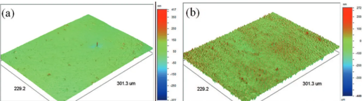
Figure 3: Surface roughness of (a) uncoated sample, (b) DLC ilm.
ball-on-plate mode, in the reciprocating manner. To validate the DLC ilm protective efect, four samples of uncoated steel were tested in comparison with eight DLC ilm coated samples, four prepared by each system. The coeicient of friction was monitored by a strain-gauge sensor, projected
to measure normal and lateral force, during 2000 cycles at
room temperature and humidity. The linear speed used was
16 mm/s, with displacement distance of 4 mm, and load
of 2N. Alumina (Al2O3) ball (4,75 mm diameter) was used
as countersample. The test was performed according to ASTM G133-0514. Optical proilometry was used to evaluate
wear test, using in a Veeco Wyko NT 1100 proilometer.
Microindentation tests were performed by using a Vickers
indenter, with maximum depth of 500 nm, 10 mN of contact force, and loading rate of 10000 nm/min. Five measurements were made in each sample. SEM images were obtained using a JEOL JSM 5310 scanning electron microscope, using
secondary electrons for the track images and backscattered
electrons for cross sectional images. The samples used for
cross sectional images were cutted by diamond cutting disc and polished by using diamond polishing paste with
diferent grain size.
3. Results and discussion
Figures 3a and 3b show surface roughness of uncoated and coated samples. Measurements of arithmetic average roughness, made with an optical proilometry, showed average roughness values of 13.2 ± 1.8 nm for substrate without DLC ilm and 33.4 ± 1.5 nm for DLC ilm. The ilm surface roughness seems to replicate substrate surface roughness. In
general, DLC surface roughness has been found to depend on the ion energy, substrate temperature, substrate materials
and ilm composition15. Figure 4 exposes the cross sectional
SEM image of DLC ilm and interface. The coating has a thickness of about 11 µm. It can be observed that about 4.5 µm is related to interface thickness, which provides a deposition rate of about 4.3 µm/h.
Raman spectroscopy results are exhibited in Table 1, according to cathode used. The obtained parameters are D and G bands position, width at half maximum (FWHM) of
G band, D and G intensities ratio (ID/IG), and hydrogenation
of the DLC ilms.
Many authors have observed a strong dependence of D and G bands position and width, and the ratio of their intensities (ID/IG) with the structural mechanical and optical
Figure 4: Cross sectional SEM image of DLC ilm and interface.
properties of the DLC ilms, and the deposition system16,17.
D and G band positions are, therefore, an indicative of DLC properties1. For both DLC ilms group obtained by the active
screen partial system and active screen system, a very small
variation is observed in bands position. The G band position
shows little variation with the interface bombardment energy, since there is a conservative behavior in the sp2 and sp3
hybridizations proportion. It was also observed that there was no signiicant diference in ID/IG ratio for both systems,
which means there were no structural changes with the interface growth variation
The DLC ilms hydrogenation did not present many variations, when each system is analyzed separately. For
coatings grown in the partial system, the hydrogen content
varied in a range from 21 to 22%. In the active screen system, the hydrogenation was about 20%. Therefore, in both cases, the ilms presented diamond-like characteristic. It can be seen that interface growth voltage variations did not afect the structural arrangement of carbon atoms, or quality of the DLC ilm, since D and G bands position, hydrogenation, ID/
IG ratio showed no signiicant variations.
However, when the Raman parameters are compared for DLC ilm obtained in each system, more signiicant changes can be observed. FWHM values of (G) and G band position measure the material disorder. A decrease of FWHM (G)
can be seen for the samples prepared by the active screen system, in relation to those prepared by the active screen
partial system. FWHM (G) is more sensitive to structural
disorder of graphitic clusters, while G band position is more
8 1386.29 1559.23 152.47 0.68 20
increases with the length and bond angle distortions between the atoms, while the topological disorder increases with the size and shape of sp2 agglomerates distribution17. This
decrease in FWHM is an evidence that the structural disorder of the active screen system prepared ilms is lower. Similar relationship between the values of FWHM (G) and disorder
was found by Kahn18.
When the G band position and the hydrogen content of DLC ilms are analyzed, it can be seen that the G band
position increases with hydrogen content decrease for DLC
ilms by using active screen system. Tamor and Vassel19 observed
a decrease in G band position and the ID/IG ratio according to the increase of sp3 atoms fraction. Noting the increase
of ID/IG ratio in coatings grown by the active screen system compared to partial system, it can be inferred that there is a
slight trend to increasing graphitic clusters size in these ilms. The ID/IG ratio increase was observed in studies of the
heat treatment efect on carbon ilms20. The authors noted
that D and G bands positions deviate to higher frequencies, and that their widths decrease as function of temperature. This was attributed to an increase in the number or size of
graphite crystals, in association with structural change of random distribution to the bond angles in a structure containing microcrystals with sp2 hybridisation21. By using the active
screen system, the high reactive ions density in plasma leads
to a tendency of increasing deposition temperature. This
occurs due to increased trapping of ions in relation to active
screen partial system. It can be inferred that this provides
an increase in the ID/IG ratio. In Figure 5 Raman spectra of
DLC ilms obtained in each system are exposed.
Hardness and elastic modulus of DLC ilms were measured by microindentation. For DLC ilms obtained by
the active screen total system, the obtained average values
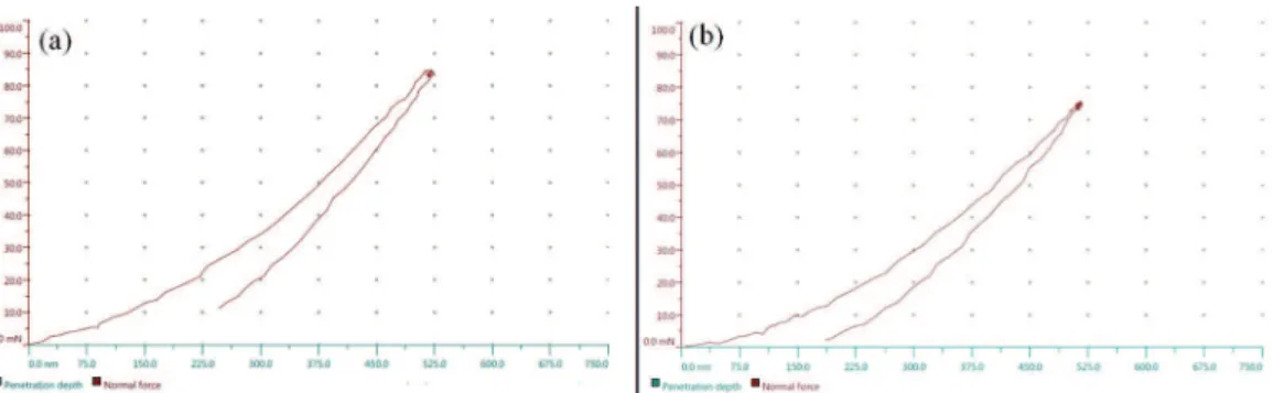
were 21.4 ± 2.6 GPa, and 176.9 ± 5.0 GPa, respectively. For DLC ilms obtained by the active screen total system, the obtained average values were 20.8 ± 1.8 GPa, and 163.3 ± 1.4 GPa, respectively. There was no diference in ilms hardness according to bias voltage variation for both systems. The load vs displacement curve is presented in Figure 6. Since
the penetration depth was prescribed in 500 nm, it ensures
that there was no substrate inluence in the measurements. Therefore, DLC ilms showed high hardness due to their
diamond-like feature, which is consistent to hydrogenation
results obtained by the Raman spectra.
DLC ilms adhesion was evaluated according to energy variation in interface deposition, for each system. Critical load values are shown in Table 2. For both samples group,
Figure 5: Raman spectra for DLC ilm obtained with (a) Active
Screen Partial System, (b) Active Screen System.
ilms adhesion increased almost linearly according to the bias voltage increase during silicon interface deposition. Similar results of enhanced adhesion were also obtained by Ward22.
When ilms adhesion is compared for each system, a
much higher performance was observed for the samples
grown in active screen system, as presented in Table 2. By
using this system, even the lowest adhesion value, which occurred for the lower bias voltage (-2 kV), was higher
than the highest value displayed for DLC ilm deposited by
using the active screen partial system, with the higher bias
Figure 6: Load vs displacement curve for DLC ilms obtained by (a) Active screen total system, (b) Active screen partial system.
Table 2: Average critical load for DLC ilms.
System Bias Voltage (-kV) Critical Load (N)
Active Screen Partial System
2 13.87 ± 0.33
4 15.82 ± 0.58
6 17.13 ± 0.39
8 18.29 ± 0.36
Active Screen System
2 28.26 ± 0.52
4 29.09 ± 0.29
6 31.07 ± 0.37
8 34.83 ± 0.43
Figure 7: Scratch test tracks (a) Delamination region wedging (b) Final track point.
is possible to observe that tensile crack was followed by chipping and coating spallation, as expected for hard coatings
over hard substrates.
Increased adhesion is explained by the use of active
screen system. In this system, which is more closed than the
active screen partial system, and the conventional cathode,
a much lower pressure can be used. At low pressures, an
opposite behavior is observed in the deposition rate for active screen systems in relation to conventional PECVD
technique. This behavior is more observed in active screen
system due to the higher interaction between electrons and
molecules. In the low pressure limit, the species distribution
rate in plasma is mainly on account of processes induced by electrons23. As the concentration of reactive species is
decreased, electrons cross section increases with electron
energy. Thus, ionization is caused by processes in which
free electrons that reach suiciently high kinetic energy collide with gas molecules promoting molecules ionization. The lower the pressure, the greater is the molecules mean free path and low regime tends to molecular, due to the fact that there are fewer molecule-molecule collisions. In
conventional system, at low pressure conditions, the electrons mean free path also becomes longer, so that the probability of electron-molecule collision decreases, reducing percentage
of molecules dissociation and ionization. The result is a reduction in deposition rate and increased plasma instability.
The use of active screen systems provided a similar hollow cathode discharge. This efect is obtained when two
parallel plates are cathodically polarized, so that an electron present between them is repeatedly repelled before leaving the inside24. Through the use of the active screen system, a
better electrons coninement efect was obtained in comparison to the active screen partial system. The system closed form is an electrons coninement region when subjected to a cathodic potential. Thus, high ions density is achieved in
this region, since each electron present in it has a greater collisions number with molecules than that outside this
region. In this case, the adhesion is inluenced by the ionic
sub-implantation, since a fraction of incident ions penetrates
the surface and densify the ilm, while others stay on the surface and contributes to the ilms thickness. Therefore, a
better ionic sub-implantation can provide better adhesion
and high hardness.
Figure 9: Friction coeicient graph of (a) uncoated sample (b)
DLC ilm.
a protective efect, as expected, which can be observed from the track proile. There were no signiicant diferences in the friction coeicient for ilms grown by the two diferent systems. The friction coeicient value for samples grown by both systems were about 0.1, while the value for uncoated steel was about 0.48. The wear rate was calculated by using ASTM G133 equations, from the area measured by optical proilometry. For uncoated samples (Figure 8a), the
wear rate was around 10-7 mm3/N.m, while for DLC coated
samples, they were around 10-9 and 10-10 mm3/N.m, for ilms
obtained by the active screen partial system (Figure 8b) and active screen system (Figure 8c), respectively. The results
values indicates the order of magnitude of the wear rate for
the tested samples.
4. Conclusions
In this work, it was possible to obtain a denser plasma
by using active screens, based in electron coninement efect in the cathode region, which probably results in a high degree of species activation. Two systems conigurations were evaluated, total and partial active screens. According to results, both systems provided DLC ilms with good structural quality and homogeneity, high hardness and good wear resistance. However, scratch tests showed diferences between the ilms obtained by the two systems. The active screen total system provided ilms with superior adhesion to the substrate, besides a smaller wear rate. This may be related to the pressure decrease, and the narrowing of ions distribution energy.
density, due to the larger number of collisions between
electrons and molecules, which increases ionization. Ion
bombardment energy during the interface growth was also studied, and presented a behavior directly proportional
to ilms adhesion. With the bias voltage increase during
silicon interface deposition, it was possible to obtain DLC
ilms better adhered to the substrate.
5. Acknowledgments
The authors would like to thank FAPESP and CNPq for inancial support.
6. References
1. Robertson J. Diamond-like amorphous carbon. Materials Science and Engineering: R: Reports. 2002;37(4-6):129-281.
2. Vetter J. 60 years of DLC coatings: Historical highlights and technical review of cathodic arc processes to synthesize various DLC types, and their evolution for industrial applications.
Surface and Coatings Technology. 2014;257:213-240.
3. Zhang W, Tanaka A, Xu BS, Koga Y. Study on the diamond-like carbon multilayer ilms for tribological application. Diamond and Related Materials. 2005;14(8):1361-1367.
4. Grill A. Diamond-like carbon: state of the art. Diamond and Related Materials. 1999;8(2-5):428-434.
5. Dalibon EL, Trava-Airoldi V, Pereira LA, Cabo A, Brühl SP. Wear resistance of nitrided and DLC coated PH stainless steel.
Surface and Coatings Technology. 2014; 255:22-27.
6. Neto VF, Oliveira MSA, Ali N, Grácio J. Time-modulated chemical vapour deposition diamonf on mould making 2738 steel. Vacuum. 2008;82(12):1346-1349.
7. Neto VF, Vaz R, Oliveira MSA, Grácio J. CVD diamond-coated steel inserts for thermoplastic mould tools — Characterization and preliminary performance evaluation. Journal of Materials Processing Technology. 2009;209(2):1085-1091.
8. Trava-Airoldi VJ, Santos LV, Bonetti LF, Capote G, Radi PA, Corat E. Tribological and mechanical properties of DLC ilm obtained on metal surface by enhanced and low-cost pulsed-DC discharge. International Journal of Surface Science and Engineering. 2007;1(4):417-428.
9. GRILL A. Electrical and optical properties of diamond-like carbon. Thin Solid Films 1999;(355-356):189-193.
10. Lin K, Li X, Sun Y, Luo X, Dong H. Active screen plasma nitriding of 316 stainless steel for the application of bipolar plates in proton exchange membrane fuel cells. International Journal of Hydrogen Energy. 2014;39(36):21470-21479.
12. Casiraghi C, Ferrari AC, Robertson J. Raman spectroscopy of hydrogenated amorphous carbons. Physical Review B.
2005;72(8):085401.
13. American Society for Testing and Materials (ASTM). C1624-05:
Standard Test Method for Adhesion Strength and Mechanical Failure Modes of Ceramic Coatings by Quantitative Single Point Scratch Testing. West Conshohocken: ASTM International; 2010. 29p.
14. American Society for Testing and Materials (ASTM). G133-05:
Standard test method for linearly reciprocating ball-on-lat sliding wear. West Conshohocken: ASTM International. 9p.
15. Peng XL, Barber ZH, Clyne TW. Surface roughness of diamond-like carbon ilms prepared using various techniques. Surface and Coatings Technology. 2001;138(1):23-32.
16. Ferrari AC, Robertson J. Raman spectroscopy of amorphous, nanostructured, diamond-like carbon, and nanodiamond.
Philosophical Transactions of the Royal Society of London. A. 2004;362(1824):2477-2512.
17. Ferrari AC, Robertson J. Interpretation of Raman spectra of disordered and amorphous carbon. Physical Review B.
2000;61(20):14095-14107.
18. Kahn M, Paskvale S, Čekada M, Schöberl T, Waldhauser W, Mitterer C, et al. The relationship between structure and mechanical properties of hydrogenated amorphous carbon ilms. Diamond and Related Materials. 2010;19(10):1245-1248
19. Tamor MA, Vassell WC. Raman “ingerprinting” of amorphous-carbon ilms. Journal of Applied Physics. 1994;76(6):3823-3830.
20. Kamiya M, Tanoue H, Takikawa H, Taki M, Hasegawa Y, Kumagai M. Preparation of various DLC ilms by T-shaped iltered arc deposition and the efect of heat treatment on ilm properties. Vacuum. 2008;83(3):510-514.
21. Adliené D, Laurikaitiené J, Kopustinskas V, Meškinis Š, Šablinskas V. Radiation induced changes in amorphous hydrogenated DLC ilms. Materials Science and Engineering: B. 2008;152(1-3):91-95.
22. Ward L, Junge F, Lampka A, Dobbertin M, Mewes C, Wienecke M. The efect of bias voltage and gas pressure on the structure, adhesion and wear behavior of Diamond Like Carbon (DLC) coatings with Si interlayers. Coatings. 2014;4(2):214-230.
23. Michelmore A, Whittle JD, Short RD. The importance of ions low pressure PECVD plasmas. Frontiers in Physics.
2015;3(3):5p.
24. Pang X, Peng H, Yang H, Gao K, Wu X, Volinsky AA. Fast deposition of diamond-like carbon films by radio frequency hollow cathode method. Thin Solid Films.