VLSI Implementation of Fixed-Point Lattice Wave Digital
Filters for Increased Sampling Rate
Meenakshi AGARWAL, Tarun Kumar RAWAT
Dept. of ECE, Netaji Subhas Institute of Technology, Sec.-3, Dwarka, New Delhi, India
[email protected], [email protected]
Manuscript received September 4, 2015
Abstract. Low complexity and high speed are the key requirements of the digital filters. These filters can be re-alized using allpass filters. In this paper, design and mini-mum multiplier implementation of a fixed point lattice wave digital filter (WDF) based on three port parallel adaptor all-pass structure is proposed. Here, the second-order allall-pass sections are implemented with three port parallel adaptor allpass structures. A design-level area optimization is done by converting constant multipliers into shifts and adds us-ing canonical signed digit (CSD) techniques. The proposed implementation reduces the latency of the critical loop by re-ducing the number of components (adders and multipliers). Three design examples are included to analyze the effective-ness of the proposed approach. These are implemented in verilog HDL language and mapped to a standard cell library in a 0.18 µm CMOS process. The functionality of the imple-mentations have been verified by applying number of different input vectors. Results and simulations demonstrate that the proposed design method leads to an efficient lattice WDF in terms of maximum sampling frequency. The cost to pay is small area overhead. The postlayout simulations have been done by HSPICE with CMOS transistors
Keywords
VLSI implementation, lattice wave digital filters, three port adaptor, canonical signed digit coefficient, fixed-point arithmetic
1. Introduction
Wave digital filters constitute a wide class of infinite impulse response (IIR) digital filters that transform an ana-log network into a topoana-logical equivalent digital filter [1]. These filters find applications in a wide variety of areas such as communication, control, biomedical engineering, audio processing and others. A major advantage of WDFs over most of other recursive filters is that they can inherit the fun-damental properties such as low coefficient sensitivity and stability under finite-arithmetic conditions [2]. Therefore, these are very attractive for Very Large Scale Integration
(VLSI) implementation. In these filters, silicon area, com-putational complexity, power consumption, and maximum achievable sampling rate are highly dependent on coefficient word length [3]. Therefore, the word length should be as short as possible, but must be sufficient to satisfy the given filter specifications [2]. Many researchers have investigated WDFs that demand low power consumption and high speed, etc., however the toughest challenge is the implementation. The VLSI implementation of WDFs using symmetric two port adaptor structure is represented in [3], [4]. In [5], the bit level systolic array method is used to increase the sampling rate to design unit element WDF and a lattice WDF using the same specifications. The systolic hardware architecture of the two filters is compared to the expected values of the integrated circuit parameters. Another method which is used to achieve significant increase in sampling rate of WDFs is most significant bit first arithmetic [6]. However, all the filters mentioned above are based on conventional two port adaptor structures also known as Richards’ allpass structure. Although M.S. Anderson et al. have compared two port and three port series adaptor realizations of second-order allpass section but VLSI implementation is not done [7]. In [8], we have proposed the VLSI implementation of lattice WDF using three port series adaptor allpass structure which pro-vides improved maximum sampling frequency compared to Richards’ allpass structure based WDFs.
In this paper, we have replaced conventional Richards’ allpass structures with three port parallel adaptor allpass structures using bit parallel arithmetic to improve the max-imum sampling rate. To increase maxmax-imum sampling fre-quency, the latency can be reduced by using low-sensitivity filters, resulting in short coefficients (low-latency multiplica-tions) and by removing unnecessary operations in the critical loop via numerical equivalent transformations [9]. However, in this work, we have mainly concerned with minimizing the critical loop latency. It is minimized by reducing the number of logic components in the critical loop. Three port parallel adaptor allpass structures can be realized with adders, de-lays and multipliers [9], [10]. The adaptor coefficients are quantized in fixed-point arithmetic. A general multiplier el-ement is very costly in full-custom VLSI implel-ementation. To solve this problem, the multiplication of a data sample
by a filter coefficient value is carried out by using a se-quence of shifts and adds and/or subtracts. For low power dissipation, the challenge is to implement the multiplier with minimum number of adders. For this purpose, it is attrac-tive to use the canonical signed digit (CSD) representation. Therefore, using CSD coefficients, the hardware cost is re-duced as well as speed is increased. The minimum number of nonzero bits are observed in CSD coefficients compared to other radix-2 representations. This reduces the number of adders/subtractors [11]. Multiple constant multiplication method is applied to implement CSD coefficients, which in turn again reduces the number of adders [9], [12].
To verify the results, VLSI implementation of lattice WDF of different orders is illustrated in Sec. 6. These filters are coded in verilog HDL language and mapped to a stan-dard cell library in a 0.18 µm CMOS process. For the same specifications, these filters are implemented using conven-tional Richards’ allpass as well as three port parallel adaptor allpass structures. This is enabled us to make a proper com-parison between their corresponding hardware realizations. The implemented filters are simulated and tested by applying different input vectors. The comparison results show that the latter design is more efficient than the conventional design in terms of the maximum sampling rate at the cost of small area overhead.
The rest of the paper is organized as follows. Section 2 describes the lattice wave digital filters. Realization of all-pass structures is presented in Sec. 3. In Sec. 4 the fixed point coefficient realization is explained. Section 5 explores the VLSI implementation. Three design examples of fixed point lattice wave digital filters using conventional Richards’ allpass and three port parallel adaptors allpass structures are presented in Sec. 6. Comparative analysis of the different approaches is also given in Sec. 6. Section 7 concludes the paper.
2. Lattice Wave Digital Filters
An explicit class of wave digital filters are called lattice wave digital filter. It is well known that the lattice WDF structures have many attractive properties such as low co-efficient sensitivity and consequently the low accuracy re-quirements for the register word length, higher dynamic range, higher overflow level, lower round-off noise, stabil-ity and good nonlinear properties under finite-arithmetic conditions where effects of rounding, truncation and over-flow are present [2], [10], [13]. Lattice WDF struc-tures find applications in lowpass-highpass filter, bandpass-bandstop filter, Hilbert transformers and quadrature mirror filters (QMF) realization [14], [15]. The resulting struc-tures are found to have minimum hardware, highly modular and less sensitive, making them suitable for signal proces-sors and VLSI implementation. The lattice WDF is repre-sented by two parallel branches, which realize allpass fil-ters. These allpass filters can be realized by using first-and/or second-order wave digital allpass sections. These
Fig. 1.Lattice wave digital filter realization ofNorder.
sections can be implemented using symmetric two port or three port networks known as adaptors in lattice WDF ter-minology and delay elements [16]. The signal flow graph of adaptor consists of multipliers and adders. The multipliers are theγcoefficients that characterize the lattice WDF. The signal flow graph of anNthorder lattice WDF is depicted in Fig. 1, where blockz−1 represents the unit delay. For any orderNthere are N2+1 stages and a maximum ofNadaptors. The transfer function of a lattice WDF can be written as the sum of transfer function of two allpass branches
H(z)= H0(z)+2 H1(z) (1)
whereH0(z)andH1(z)are the transfer functions of stable
allpass filters of ordersMandN, respectively. In case of low pass filters,M =N−1 orM =N+1 so that M+Norder of overallH(z)is odd. These filters can be realized in many different ways [17].
In this work, we only consider the cascade realization of the first- and second-order allpass sections. A first-order allpass section can be realized using Richards’ structure, where a symmetric two port adaptor and a delay element are used [9]. The second-order allpass section can be re-alized using a cascade of two first-order Richards’ allpass structures. A second-order allpass section is also realized us-ing a three port parallel adaptor and two delay elements [1]. The detailed discussion of the first- and second-order all-pass sections is given in Sec. 3. These allall-pass sections are recursive structures. Generally, recursive structures require a smaller number of arithmetic operations per sample than their nonrecursive counterparts. One limitation of the re-cursive structure is the maximum sampling frequency fmax
fmax= 1
Tmin =min
( N
i Ttot
)
(2)
whereTmin is the minimum sampling time,Ttotis the total
latency of the arithmetic operations and Ni is the number
of delay elements in the directed loop i [18]. The loop(s) that determines the maximum sampling frequency is called the critical loop(s). The digital filters with high maximum sampling frequency are suitable candidates of low power and high speed applications. The reason is that if required sam-pling rate is less than the maximum samsam-pling rate, the excess speed can be utilized to reduce the power consumption via power supply voltage scaling techniques [17], [18]. The area can be minimized by clever hardware design [19]. From (2), we observe two factors that are affecting the maximum sam-pling rate. The first factor is the number of delay elements in the critical loop and second is the total latency in the critical loop. The maximum sampling frequency can be increased by increasing the number of delay elements in the critical loop or by minimizing the critical loop latency. In this work, we have mainly concerned with minimizing the critical loop latency. It is minimized by reducing the number of logic components in the critical loop. It is further minimized by reducing the critical delay at logic level.
3. Realization of Allpass Structures
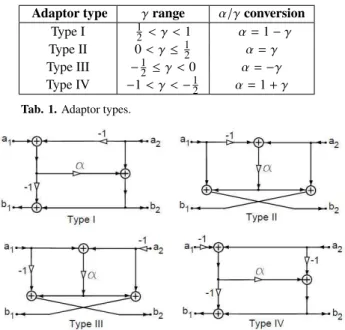
A lattice WDF, is realized by the two parallel allpass branches whose output are summed to produce the filter out-put. These allpass filters are replaced by the cascaded first-and second-order allpass sections implemented using either symmetric two port or three port parallel adaptor structures and delay elements. A first-order two port adaptor has a co-efficient value (γ) which controls the response of the allpasssection. This adaptor requires a single multiplication and three additions each. Lattice WDFs use four types of sym-metric two port adaptors as its building blocks depending on the value ofγcoefficient. The signal flow graphs of four sin-gle multiplier symmetric two port configurations are shown in Fig. 2. These adaptor coefficients γmay be guaranteed to fall into the interval−1 < γ < 1 [13]. Methods to cal-culate these coefficients from the design specifications have been discussed in [13]. The different adaptor structure can be chosen depending on the value ofγcoefficient as given in Tab. 1.
In these adaptor structures, the coefficient value of the actual multiplier (α) to be implemented is always positive and less than or equal to half, that is, 0 ≤ α ≤ 12. To
de-sign allpass section from these adaptor structures, one port is terminated with the delay element. Generally, the transfer function of a first-order allpass section is given by
H(z)= t0+z
−1
1+t0z−1 (3)
and for a second-order allpass section
H(z)= t2+t1z
−1
+z−2 1+t1z−1+t2z−2
(4)
Adaptor type γrange α/γconversion
Type I 12 < γ <1 α=1−γ
Type II 0< γ≤12 α=γ
Type III −12 ≤γ <0 α=−γ
Type IV −1< γ <−12 α=1+γ
Tab. 1.Adaptor types.
Fig. 2.Signal flow graph of four symmetric two-port adaptor.
wheret0 = −γ0,t1 = (γ1 −1)γ2 andt2 = −γ1 [13]. The
first- and the second-order allpass sections realized using symmetric two port adaptors are called as Richards’ allpass structure. Different symmetric two port adaptor structures can be chosen depending on the value of γ coefficient as given in Tab. 1. The second-order allpass sections are also realized using three port parallel adaptor and delays, called as three port parallel adaptor allpass structure.
3.1 Richards’ Structures
First-order Richards’ allpass structure is composed of the symmetric two-port adaptor and a delay element, as shown in Fig. 3. The signal flow graph of the conventional symmetric two-port adaptor forming the first-order Richards’ allpass structure is described by the following equations
b1=α(a2−a1)+a2, (5)
b2 =α(a2−a1)+a1 (6)
wherea1anda2are the inputs andb1andb2are the outputs.
The critical loop is shown by thick lines in Fig. 3. Since this critical loop has one multiplier, two adders and one delay element, the total latencyTtotis equal toTm,α+2Ta, where
Tm,αis the time delay for the multiplier andTais the adder
delay [9], [19] andNi=1. Using (2), the maximum sampling
frequency fmaxof this structure is given by
fmax= 1
Tm,α+2Ta
. (7)
Similarly, the second-order Richards’ allpass structure is cascade of the two first-order allpass structures and is shown in Fig. 4. Since this critical loop has two multi-pliers, four adders and one delay element, Ttot is equal to
Tm,α1+Tm,α2+4Ta, where,Tm,α1 andTm,α2are the time
de-lays for the two multipliers andTais the adder delay [9] and
fmax= 1
Tm,α1+Tm,α2+4Ta
. (8)
3.2 Three Port Parallel Adaptor Allpass
Struc-ture
A second-order three port parallel adaptor allpass struc-ture is shown in Fig. 5. The transfer function of this section is given by [18]
H(z)= (1
−β1−β2)+(β1−β2)z−1−z−2 −1+(β1−β2)z−1
+(1−β1−β2)z−2 (9) where β1 and β2 are the adaptor coefficients. Comparing
with (4) we get the relationship between the adaptor coeffi-cients to [18]
β1= (1
−γ1)(1+γ2)
2 , β2=
(γ1−1)(γ2−1)
2 . (10)
It is observed from Fig. 5 that one of the two loops can be the critical loop. Assuming same number of fractional bits ofβ1andβ2, loop 1 has one multiplier, three adders and
one delay element. While, loop 2 has one multiplier, four adders and one delay element. Since loop 2 contains more components, therefore, it is considered as the critical loop. The maximum sampling frequency of this structure is given by
fmax= 1
Tm+4Ta
. (11)
We observe that the critical loop of the Richard’s second-order allpass structure contains two multipliers and four adders as shown in Fig. 4. However, a three port par-allel adaptor allpass structure contains only one multiplier and four adders. For the latter realization, the price to pay is somewhat longer coefficient wordlength to meet the filter specifications. However, it is found that the three port adaptor coefficients typically require one extra bit to match the per-formance of the two port realization for a given coefficient wordlength [7].
Fig. 3.First-order Richards’ allpass structure with critical loop.
Fig. 4.Second-order Richards’ allpass structure with critical loop.
Fig. 5.A three port parallel adaptor allpass structure.
4. Fixed-Point Coefficients
In this work, we concentrate on coefficient quantization in fixed point arithmetic. The goal of a fixed-point arith-metic is to maximize the filter performance and minimize finite-word-length effects [20–24]. It is desired that the coef-ficient valuesγkfork=0,1,2, . . . ,(M+N−1)are expressed as the following fixed-point binary numbers [10]
−x0+
T X
r=1
xr2
where xr forr = 0,1, . . . ,B is either 0 or 1. Here x0 is
the sign bit. For negative numbers sign bit is equal to one, whereas for non-negative numbers it is equal to zero. The goal is to express all the filter coefficient values in the above form with the minimum number of fractional bits B. For efficient multiplier implementation in full-custom VLSI im-plementation, the multiplication of a data sample by a filter coefficient value is carried out by using a sequence of shifts and adds and/or subtracts. In this case, it is desired to express the coefficient values in the following form
R X
r=1
xr2−Pr (13)
where eachxris either 1 or−1 and thePR’s are nonnegative
integers in the increasing order. The goal is to find all the coefficient values with minimum number ofR, the number of power-of-two terms and the maximum number of shiftsPR is made as small as possible [10]. For this purpose, it is at-tractive to use the canonic-signed-digit (CSD) representation. This representation has three digits,−1, 0 and+1 as opposed
to the two’s-complement representation which has only two digits, 0 and+1 [10]. The number of adders and/ or
subtrac-tors required to realize a CSD coefficient is one less than the number of nonzero digits in this coefficient representation form [25].
5. VLSI Implementation
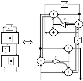
In this section, VLSI implementation of lattice WDF is presented. These filter structures are realized using adders, multipliers and delay elements. The multiplication of a data sample with each filter coefficient value is performed using a sequence of shift and add and/or subtract operations which is called as multiplierless implementation. Hence, the fil-ters are implemented only with the adders and/or subtractors and delay elements. For minimum adder implementation the coefficients are realized in CSD representation. Steps followed for the implementation are given in Fig. 6 [26]. Mentor Graphics ASIC Design Kit (ADK) tools are used for IC flow, synthesis to standard cells and IC physical design and simulation.
6. Design Examples
To show the design process three examples of the lattice wave digital structure and their multiplierless implementation are presented. In these implementations Richards’ and three port parallel adaptor allpass structures are used. The input samples wordlength is chosen as 8-bits. The coefficients wordlength is 9-bits and 10-bits for Richards’ and three port parallel adaptor allpass sections, respectively. The perfor-mance of the two implementations are compared in terms of maximum sampling frequency and area.
Fig. 6.Flow Diagram of VLSI Implementation.
Example 1:
Specifications of the Chebyshev low-pass lattice WDF are as follows [16, p. 12]: Sampling frequencyF = 16 kHz, Pass-band edge frequencyfp= 3.4 kHz, Stopband edge frequency fs= 4.5 kHz, Passband rippleAp= 0.5 dB, Stopband attenu-ation As=50 dB and Filter orderN= 9. We see from Fig. 1 that 9thorder lattice WDF is composed of one first- and four
second-order allpass sections [9]. Its transfer function is given by
H(z)=12
−0.66771
+z−1
1−0.66771z−1
!
0.61883−0.87844z−1
+z−2
1−0.87844z−1+0.61883z−2
!
0.91914−0.41780739z−1
+z−2
1−0.41780739z−1+0.91914z−2
!
+ 0.49630
−1.19393z−1
+z−2
1−1.19393z−1+0.49630z−2
!
0.76628−0.57968z−1
+z−2
1−0.57968z−1+0.76628z−2
! .
(14) For multiplierless implementation of the lattice WDF,
γcoefficients, adaptor type,αcoefficients (for Richards’ im-plementation), βcoefficients (for three port parallel adaptor implementation) and their CSD representations are given in Tab. 2. For Richards’ implementation, blocks of first- and second-order allpass sections are replaced with their equiva-lent signal flow graphs depicted in Fig. 3 and 4, respectively. The minimum sampling periodsTmin of individual allpass
sections are as follows
Tminα0 =Tm+2Ta,
Tminα1α2 =2Tm+5Ta,
Tminα3α4 =2Tm+5Ta,
Tminα5α6 =2Tm+5Ta,
and Tminα7α8 =2Tm+4Ta.
(15)
The minimum sampling periodTmin of the overall filter, is
given by
Tmin=max(Tminα0,Tminα1,α2,Tminα3,α4,Tminα5,α6,Tminα7,α8 )
γi,0≤i≤8 Adaptor αj,0≤j≤8 αC S D βk,1≤k≤8 βC S D type
0.667713527 1 0.33228647 0.01010101 − −
−0.49630558 3 0.49630558 0.10000001 1.34511717 1.010100000
0.797917736 1 0.202082263 0.01010100 0.1511885 0.001010010 −0.618835168 4 0.381164832 0.10100010 1.24864118 1.0100000010
0.542641521 1 0.457358479 0.10010101 0.370194 0.101000010 ˘0.766286584 4 0.233713416 0.01000100 1.17298493 1.010101000 0.328193215 2 0.328193215 0.01010100 0.5933016 0.101010000 −0.919144204 4 0.080855796 0.00010101 1.1684758 1.010101010
0.217705053 2 0.217705053 0.01001000 0.7506684 1.010000000
Tab. 2.Low-pass filter coefficients (Example 1).
The maximum sampling frequency fmaxis given by
fmax= 1 Tmin =
1 2Tm+5Ta
. (17)
For multiplierless implementation, fmaxis given by the following equation
fmax=min 1 2Ta+2Ta
, 1
3Ta+5Ta
, 1
4Ta+5Ta
, 1
3Ta+5Ta
,
1 3Ta+4Ta
= 1
9Ta
. (18)
To implement a low-pass lattice WDF using three port parallel adaptors, blocks of second-order allpass sections are replaced with three port parallel adaptor allpass structures, shown in Fig. 5. Although, (α0) is implemented with the Richards’ first-order allpass structure. Thefmaxof the overall filter is determined by one of the critical loops of this allpass section. The fmax in terms ofTm andTa for each of these allpass sections is same as given in (11). The multipliers are implemented with a network of shift and add and/or subtract operations using CSD coefficients. βcoefficients and their CSD equivalents are given in Tab. 2. For the multiplierless implementation, fmaxis given by
fmax=min
fmaxα0,fmaxβ1β2,fmaxβ3β4,fmaxβ5β6,fmaxβ7β8
=min 1 6Ta , 1 6Ta , 1 5Ta , 1 6Ta = 1 6Ta . (19)
Comparing equations (18) and (19), we observe that fmaxis improved by approximately 49 % by reducing critical delay. The filters are implemented in CMOS VLSI design and results are summarized in Tab. 3. Here, fmax for three port adaptors allpass based lattice WDF is improved by 15 % compared to Richards’ allpass based filter. However, the area is increased by 24 %.
fmax Area(mm2) Number of
gates Richards’ allpass 58.5 MHz 2.952 2304 Three port adaptor 67.6 MHZ 3.669 2887
allpass
Tab. 4.Comparison offmaxand area of low-pass lattice WDF based on Richards’ and three port parallel adaptor struc-tures (Example1).
Example 2:
Consider an elliptic low-pass lattice WDF with the following specifications [13].F= 16 kHz, fp= 3 kHz, fs= 5 kHz,Ap
= 1.0 dB , As = 40 dB, Filter type = Chebyshev, and N=5.
From Fig. 1, we observe that 5thorder lattice WDF consists of one first- and two second-order allpass sections. For the above specifications, transfer function is given by
H(z)=1 2
−0.6338
+z−1 1−0.6338z−1
0.8260−0.68566z−1
+z−2 1−0.68566z−1
+0.8260z−2
+
0.5372−1.01532z−1
+z−2 1−1.0153z−1
+0.5372z−2
.
(20)
For multiplierless implementation of the lattice WDF,
γ coefficients, adaptor type, α coefficients (for Richards’ implementation),βcoefficients (for three port parallel adap-tor implementation) and their CSD representations are given in Tab. 4. For Richards’ structure implementation, fmax is given by
fmax=min
1 2Ta+2Ta
, 1
4Ta+5Ta
, 1
3Ta+4Ta =min 1 4Ta , 1 9Ta , 1 7Ta = 1 9Ta . (21)
To implement the low-pass lattice WDF using three port parallel adaptors, the fmaxin terms ofTm andTafor each of these allpass sections, is same as given in (11). Theβ coeffi-cients and their CSD equivalents are given in Tab. 4. For the multiplierless implementation, fmaxis given as follows
fmax=min
fmaxα0,fmaxβ1β2,fmaxβ3β4
=min 1 4Ta , 1 7Ta , 1 6Ta = 1 7Ta . (22)
Comparing equations (21) and (22) shows that fmaxis improved by approximately 28.5 % by reducing critical loop delay. The filters are implemented in CMOS VLSI design to verify the results and are summarized in Tab. 5. Here,fmaxfor three port adaptors allpass based lattice WDF is improved by approximately 16.5 % compared to Richards’ allpass based filter. However, the area is increased by 18 %.
γi,0≤i≤4 Adaptor αj,0≤j≤4 αC S D βk,1≤k ≤4 βC S D type
0.6338 1 0.3662 0.10100010 − −
−0.5372 4 0.4628 0.1000101 1.2762603 1.010010101 0.6605 1 0.3395 0.10101001 0.26093 0.010001010
−0.8360 4 0.1740 0.01010101 1.262709 1.010001001 0.3755 1 0.3755 0.10100000 0.573291 0.10010101
Tab. 3.Coefficients of low-pass WDF filter (Example 2).
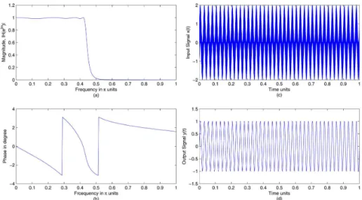
Fig. 7.Magnitude response (a), phase response (b), input signal (c), filtered output (d).
fmax Area(mm2) Number of gates Richards’ allpass 70.0 MHz 1.934 1476 Three port adaptor 81.6 MHZ 2.285 1698
allpass
Tab. 6.Comparison offmaxand area of low-pass lattice WDF
(Example 2).
Example 3:
Consider an elliptic low-pass lattice WDF with the following specifications [13]. F=16 kHz, fp = 3.4 kHz, fs= 4.6 kHz, Ap= 0.2 dB, As=65 dB, Filter type= Cauer, and Filter order N= 7. From Fig. 1, we observed that the 7th order lattice
WDF requires one first- and three second-order allpass sec-tions. For given filter specifications, the transfer function is obtained as
fmax Area(mm2) Number of gates Richards’ allpass 63.1 MHz 2.472 1865 Three port adaptor 71.3 MHz 2.966 2595
allpass
Tab. 7.Comparison offmaxand area of low-pass lattice WDF
(Example 3).
H(z)=12
−0.5190
+z−1
1−0.5190z−1
! 0
.66872−0.557752z−1
+z−2
1−0.55772z−1+0.66872z−2
!
+ 0.40441
−0.853474z−1
+z−2
1−0.853474z−1+0.40441z−2
! 0
.89613−0.39193z−1
+z−2
1−0.39193z−1+0.89613z−2
! .
(23) The magnitude and phase response of the designed fil-ter are depicted in Fig. 7(a) and 7(b). When an input signal x(t) =sin(80πt)+sin(12000πt)is applied to the filter, its
γi,0≤i≤6 Adaptor αj,0≤j≤6 αC S D βk,1≤k ≤6 βC S D type
0.51290 1 0.4871 0.10000101 − −
−0.40441 3 0.40441 0.10101000 0.8337626 1.001010101 0.60271 1 0.3922 0.10100100 0.2618522 0.010001010
−0.66872 4 0.3313 0.1010101 1.113236 1.001001010 0.33424 2 0.33424 0.10101010 0.5554835 0.100100100
−0.89613 4 0.1038 0.00100101 1.14402056 1.001001010 0.20669 2 0.2067 0.01010101 0.69502645 1.0101001
output is y(t) = sin(80πt). Both x(t) and y(t) are shown in Fig. 7(c) and 7(d). The responses shown in Fig. 7 are illustrated using MATLAB tool.
For multiplierless implementation of the lattice WDF,
γcoefficients, adaptor type,αcoefficients (for Richards’ im-plementation), βcoefficients (for three port parallel adaptor based implementation) and their CSD representations are given in Tab. 6. For Richards’ implementation, fmaxis given by
fmax=min
1 2Ta+2Ta
, 1
4Ta+5Ta
, 1
4Ta+4Ta
, 1
4Ta+4Ta
=min
1 4Ta
, 1
9Ta
, 1
8Ta
, 1
8Ta
= 1
9Ta
. (24)
To implement a low-pass lattice WDF using three port parallel adaptors, the fmaxin terms ofTm andTafor each of these allpass sections, is same as given in (11). βcoefficients and their CSD equivalents are given in Tab. 6. For multipli-erless implementation, minimum fmaxof the overall filter is given by
fmax=min
fmaxα0,fmaxβ1β2,fmaxβ3β4,fmaxβ5β6
=min
1 4Ta
, 1
7Ta
, 1
6Ta
, 1
6Ta
= 1
7Ta
. (25)
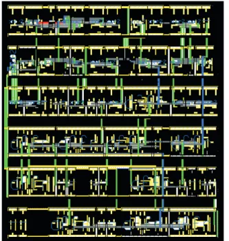
Comparing of equations (24) and (25),fmaxis improved by approximately 28.5 % by reducing critical loop delay. The filters are implemented in CMOS VLSI design and results are summarized in Tab. 7. CMOS layout diagram of the WDF us-ing three port adaptor allpass structure is depicted in Fig. 8. The fmax for three port adaptors based lattice WDF is im-proved by 13 % compared to Richards’ structure based filter. However, the area is increased by 20 %.
7. Conclusion
In this paper, novel approach to design a fixed-point lattice WDF for increased maximum sampling frequency is presented. It is increased by reducing the number of logic components in the critical loop resulting reduced critical de-lay of the logic components. Second-order three port parallel adaptor allpass section has smaller number of logic compo-nents in their critical loop than Richards’ allpass section. For the given examples the maximum sampling frequency is improved by using three port parallel adaptor allpass than the conventional Richards’ allpass structures. Three design examples are included here of different order lattice WDF. Three port parallel adaptor and Richards’ allpass structures based lattice WDF meeting the same filter specifications were designed and implemented using logic synthesis from Ver-ilog HDL description. Lattice WDF structures were evalu-ated with respect to throughput and arithmetic complexity. The efficient implementation of lattice WDF is presented using 0.18 μm CMOS process in a standard cell library.
Fig. 8.Layout Diagram of lattice WDF implemented with three port adaptor allpass structure.
References
[1] JOHANSSON, H., WANHAMMAR, L. Wave digital filter struc-tures for high-speed narrow-band and wide-band filtering. IEEE Transaction of Circuits and Systems-II: Analog and Digital Signal Processing, 1999, vol. 46, no. 6, p. 726–741. ISSN: 1057-7130. DOI: 10.1109/82.769781
[2] FETTWEIS, A. Wave digital filters: Theory and practice. InProceed-ings of the IEEE. 1986, p. 270–327. DOI: 10.1109/PROC.1986.13458
[3] WICKS, T., SUMMERFIELD, S. VLSI implementation of high speed wave digital filters based on a restricted coefficient set. InIEEE Inter-national Symposium on Circuits and Systems (ISCAS ’93). Chicago (USA), 1993, p. 603–606. DOI: 10.1109/ISCAS.1993.393793
[4] SUMMERFIELD, S., WICKS, T., LAWSON, S. Design and VLSI architecture and implementation of wave digital filters using short signed digit coefficients. InIEE Proceedings-Circuits Devices Sys-tems. Oct. 1996, p. 259–266. DOI: 10.1049/ip-cds:19960705
[5] SUMMERFIELD, S., LAWSON, S. The design of wave digital filter using fully pipelined bit-level systolic arrays.Journal of VLSI Signal Processing, Sep. 1990, vol. 2, p. 51-–64. DOI: 10.1007/BF00931036
[6] SINGH, R. J., MCCANNY, J. V. High performance VLSI architec-ture for Wave Digital Filtering.Journal of VLSI Signal Processing, 1992, vol. 4, p. 269–278. DOI: 10.1007/BF00930640
[7] ANDERSON, M. S. , SUMMERFIELD, S., LAWSON, S. Realiza-tion of lattice wave digital filters using three-port adaptors.Electronics Letters, 1995, vol. 31, no. 8, p. 628–629. DOI: 10.1049/el:19950459
[8] AGARWAL, M., RAWAT, T. K. VLSI implementation of lattice wave digital filters using fixed point arithmetic for increased max-imum sampling frequency.Journal of Computer Engineering and Informention Technology, 2015, vol. 4, no. 4. DOI: 10.4172/2324-9307.1000138
[9] OHLSSON, H. Studies on implementation of digital filters with high throughput and low power consumption.Thesis no. 1031, Linköping University, Sweden, 2003.
[10] YLI-KAAKINEN, J., SARAMÄKI, T. A systematic algorithm for the design of lattice wave digital filters with short-coefficient wordlength. IEEE Transaction on Circuits and Systems-I, 2007, vol. 54, no. 8, p. 1838–1851. DOI: 10.1109/TCSI.2007.902513
[11] OHLSSON, H., GUSTAFSSON, O., JOHANSSON, H., et al. Im-plementation of bit-parallel lattice wave digital filters with increased maximal sample rate. In Proceedings of 8th IEEE Conference on Electronics, Circuits and Systems (ICECS), 2001, vol. 1, p. 71–74. DOI: 10.1109/ICECS.2001.957672
[12] JOHANSSON, K., GUSTAFSSON, O., WANHAMMAR, L. Mul-tiple constant multiplication for digit-serial implementation of low power FIR filters.WSEAS Transaction on Circuits and Systems, 2006, vol. 5, no. 7, p. 1001–1008.
[13] GAZSI, L. Explicit formulas for lattice wave digital filters.IEEE Transactions on Circuits and Systems, 1985, vol. 32, no. 1, p. 68–88. DOI: 10.1109/TCS.1985.1085595
[14] AGARWAL, M., BARSAINYA, R., RAWAT, T. K. FPGA im-plementation of Hilbert transformer based on lattice wave digi-tal filters. In Proceedings of 4th IEEE Conference on Reliability, Infocom Technologies and Optimization (ICRITO). 2015, p. 1–5. DOI: 10.1109/ICRITO.2015.7359331
[15] BARSAINYA, R., AGARWAL, M., RAWAT, T. K. Multiplier-less implementation of quadrature mirror filter. InProceedings of 4th IEEE Conference on Reliability, Infocom Technologies and Optimiza-tion (ICRITO). 2015, p. 1–6. DOI: 10.1109/ICRITO.2015.7359328
[16] VENKAT, K.Wave Digital Filtering Using MSP430 – Application Report, Texas Instruments. 25 pages. 2006.
[17] WANHAMMAR, L.DSP Integrated Circuits. New York (USA): Aca-demic Press, 1999.
[18] GUSTAFSSON, O., WANHAMMAR, L. Maximally fast schedul-ing of bit-serial lattice wave digital filters usschedul-ing three-port adaptor allpass sections. InProceeding of Nordic Signal Processing Sympo-sium. 2000, p. 441–444.
[19] OHLSSON, H., WANHAMMAR, L. Implementation of bit-parallel lattice wave digital filters. InProceeding of Swedish System-on-Chip Conference. 2001, p. 71–74.
[20] GOETTE, J. On fixed-point filter realizations.Bern University of Ap-plied Sciences, Biel/Bienne Institute of Human Centered Engineering - microLab, Feb. 2015.
[21] VOLKOVA, A., HILAIRE, T. Fixed-point implementation of lattice wave digital filter: comparison and error analysis. InProceedings of the 23rd European Signal Processing Conference (EUSIPCO). 2015, p. 1118–1122. DOI: 10.1109/EUSIPCO.2015.7362557
[22] YATES, R.Practical Considerations in Fixed-Point FIR Filter Im-plementations. Sep. 2010.
[23] MATHWORKS. Fixed-Point Filter Design in MATLAB (documentation). [online] Cited 2015-08-14. Available at: http://in.mathworks.com/help/dsp/ug/fixed-point-filter-design.html
[24] DOLECEK, G. J., LADDOMADA, M. An improved class of multiplierless decimation filters: Analysis and design. Digi-tal Signal Processing, 2013, vol. 23, no. 5, p. 1773–1782. DOI: 10.1016/j.dsp.2013.05.011
[25] Constant Multiplier Optimization to Reduce Area (MAT-LAB Examples). [Online] Cited 2015-08-20. Available at: http://www.mathworks.com/examples/matlab-hdl-coder/1311-constant-multiplier-optimization-to-reduce-area
[26] NELSON, B. Test Generation and Design for Test (Mentor Graphics) Document. [Online] Cited 2016-03-10. Available at: http://www.eng.auburn.edu/ strouce/class/elec6970/NelsonBIST.pdf
About the Authors . . .
Meenakshi AGARWALreceived her B.Tech degree in Elec-tronics and Telecommunication Engineering in the year 2005 from CERT, UPTU University, Lucknow. She received her M.Tech, exemplary performance in 2009. She is currently pursuing Ph. D. from Netaji Subhas Institute of Technology (NSIT), University of Delhi.