Gap Energy Studied by Optical Transmittance in Lead Iodide
Monocrystals Grown by Bridgman’s Method
N. Veissid*, C.Y. An, A. Ferreira da Silva, J.I. Pinto de Souza
Instituto Nacional de Pesquisas Espaciais - INPE/LAS, C.P. 515, 12201-970 São José dos Campos, SP - Brazil
Received: February 27, 1999; Revised: July 15, 1999
The bandgap energy as a function of temperature has been determined for lead iodide. The monocrystal was obtained in a vacuum sealed quartz ampoule inside a vertical furnace by Bridg-man’s method. The optical transmittance measurement enables to evaluate the values of Eg. By a fitting procedure of Eg as a function of temperature is possible to extract the parameters that govern its behavior. The variation of Eg with temperature was determined as: Eg(T) = Eg(0) - αT2/(α + T), with: Eg(0) = (2.435 ± 0.008) eV, α = (8.7 ± 1.3) x 10-4eV/K and α = (192 ± 90) K. The bandgap energy of lead iodide at room temperature was found to be 2.277 ± 0.007 eV.
Keywords:optical properties, lead iodide, Bridgman’s Method
1. Introduction
Lead iodide crystals has been studied as a very promis-ing material with large technological applicability as room temperature nuclear radiation detectors1-3. Lead iodide (PbI2) is a wide band gap energy semiconductor (Eg = 2.2 eV) very similar to mercuric iodide (HgI2)4, but it presents more attractive physical properties to be used as a substrate for the fabrication of detectors. For example, its lower vapor pressure compared to the HgI2 contributes for a higher stability as detectors1. Devices manufactured with this material show good performance also at temperatures higher than room temperature (about 100 °C) and for long periods (3 months)2.
The bandgap energy of lead iodide has been reported by several authors5-8 and its value is found to be between 2.2 eV and 2.55 eV, for pure and doped samples. There are several methods to estimate the bandgap energy of lead iodide, as photoluminescence, electrical conductivity and optical absorption, among others. Here we have used the optical transmittance measurements in a way to investigate the temperature dependence of the band gap energy.
The crystal of lead iodide was grown by Bridgman’s method5.
2. Experimental
In the present investigation, the starting material for crystal growth is crystalline powder from Johnson Matthey 99.9999% in purity (metal basis). This material was
puri-fied using a horizontal float zone purification heater, where a vacuum sealed ampoule (10-5 Torr) had 20 passes at a velocity of 1mm/h. In a semiquantitative analysis, made by infrared absorption, around 1% of hydrocarbons was found in the material, after the float zone purification that reduced the content of carbon atoms. The purified material, 100 grams inside a vacuum sealed quartz ampoule (2 mm in thickness, 18 mm in inner diameter and 25 cm in length), was maintained at 430 °C for 48 h to obtain an homogene-ous compound.
For single crystal preparation, another tipped-end quartz ampoule (8 mm in inner diameter and 20 cm in length) was loaded with 10 g of the reacted PbI2 and sealed under a vacuum of 10-5 Torr. The ampoule was placed in a vertical furnace for growing PbI2 crystals by Bridgman’s method. After furnace heating, the upper temperature (start-ing ampoule position) was maintained at about 40 °C above the melting point (408 °C) of the compound. The crystal growth was performed by dropping the ampoule at a rate of about 2 mm/h through a cooling gradient of 10 °C/cm. This growth results in a PbI2 single crystal (30 mm length and 8 mm diameter) with the c-axis oriented perpendicular to the growth axis. After a homogenization process, thermal an-nealing at 250 °C during 24 h, the lead iodide material has the visual aspect of amber.
The crystal was cleaved perpendicular to c-axis and each slice has about 0.5 cm2 in area, with thickness around 0.5 mm. The optical transmittance (OT) measurements
e-mail: [email protected]
were made using the electrical signal of a solar cell, work-ing in the short circuit current mode. This solar cell, very well characterized, is used in the solar cell experiment of the first Brazillian satellite9-11. The OT system consists of a xenon lamp of 1 kW, a monochromator, a chopper in a frequency of 35 Hz, a lock-in amplifier, a home made liquid nitrogen cryostat and the sensor-sample aluminium con-tainer inside of cryostat. The apparatus is monitored by a computer, which displays monochromator wavelength, electrical current of solar cell and temperature. The cryostat works in the temperature range 90 K-340 K and the mono-chromatic light beam reaches the sensor through a 5mm diameter (glass window) in the aluminium container. The solar cell signal is first measured without the lead iodide and, then, with the sample. The transmittance value of sample (T) is determined as a percentage of the signal, i.e. as the rate of signal value without sample by the value with sample and multiplied by 100. The temperature sensor is a K-type thermocouple attached in the sensor-sample alu-minium structure.
3. Results and Analysis
Figure 1 shows the temperature dependence of the optical transmittance curves of lead iodide obtained by the rating of electrical signal of solar cell in short circuit current mode, without sample by the signal with the sample in front of sensor. Rigorously, the bandgap energy should have been calculated from the optical absorbance measurements but, in this work, the maximum transmittance and the minimum absorbance are considered at the same wave-length, because the semiconductor reflectivity is constant at this wavelength4. So, Eg(T) is calculated from the deriva-tive curve of OT presented in Fig. 1. These derivaderiva-tive curves, in the wavelength range of interest are presented in Fig. 2. The peak value in each curve is associated to the optical band-gap energy Eg5, where it is calculated using the following equation:
Eg= hc
λmax
(1)
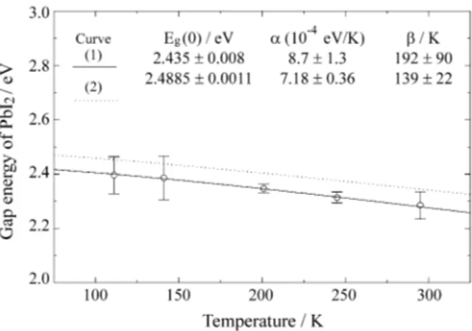
where h is the Planck constant, c is the light velocity and λmax is the wavelength in the maximum of the derivative curve. The Eg values are determined using Eq. (1), where λmax is obtained by a least square fitting procedure of the parable. In Fig. 3 these values are presented with the correspondent standard deviations as a function of temperature. Using another numerical least square fitting procedure is possible to extract the temperature dependence of the energy gap for many semiconductors from the Varshni relation12.
Eg(T)=Eg(0)− αT 2
β+T (2)
where Eg(0) is the bandgap energy at T = 0K and α and α are the so-called Varshni coefficients. The smooth curves shown in Fig. 3 were obtained by fitting of Eq. (2) to the data sets. The parameters values offering the best fits are
280 Veissid et al. Materials Research
Figure 1. Optical transmittance of lead iodide sample at several tempera-tures.
Figure 2. Fitted derivative curves in the wavelength range of the maxi-mum value of optical transmittance for lead iodide grown by Bridgman’s method.
presented with the corresponding standard deviations. For this work, we have found Eg(0) = (2.435 ± 0.008)eV, α = (8.7 ± 1.3) x 10-4 eV/K and α = (192 ± 90) K. It is worth to mention that the value of α for most of semiconductors is around 10-4 eV/K14. The Eg value as a function of temperature, determined by photoluminescence technique, for a sample of lead iodide of this same ingot can be compared with the present results13. The values obtained by photoluminescence are Eg(0) = (2.4885 ± 0.0011) eV, α = (7.18 ± 0.36) x 10-4 eV/K andα = (139 ± 22) K. Eg(T) is plotted in Fig. 3 as curve number (2).
4. Conclusions
The band gap energy expected from good undoped lead iodide monocrystals is higher than 2.55 eV at room temperature. The sample studied has Eg about 2.3 eV, value obtained by both methods (photoluminescence and transmittance). We concluded that the purification pro-cess (float zone) used to eliminate the based carbon atoms impurities, was not effective or perhaps it will be necessary to repeat the purification process several times more. We are intended to obtain new ingots and this point of view will be considered. The impurities charac-terization and the purification process will be studied in future works.
Lead iodide is a promising semiconductor material for the manufacturing of room temperature ionizing radiation detectors. Crystals grown by Bridgman’s method present good semiconductor characteristics as confirmed by the optical absorbance.
Acknowledgments
The authors (NV and AFS) would like to acknowledge support of the Conselho Nacional de Desenvolvimento Científico e Tecnológico (CNPq-Brasil).
References
1. George, M.A.; Azoulay, M.; Jayatirtha, H.N.; Biao, Y.; Burger, A.; Collins, W.E.; Silberman, E. J. Crystal Growth, v. 137, p. 299, 1994.
2. Lund, J.C.; Shah, K.S.; Squillante, M.R.; Moy, L.P.; Sinclair, F.; Entine, G. Nuclear Inst. and Methods in Phys. Res., v. A283, p. 299, 1989.
3. Shoji, T.; Ohba, K.; Suchiro, T.; Hiratate, Y. IEEE Trans. Nucl. Sci., v. 42, p. 659, 1995.
4. Silva, A.Ferreira da ; Veissid, N.; An, C.Y.; Caetano de Souza, J.; Silva, A.V. Batista da; Farias, P. César; Cruz, M.T.F. da J. Appl. Phys. v. 78, n. 9, p. 5822, 1995. 5. Ferreira da Silva, A.; Veissid, N.; An, C.Y.; Pepe, I.;
Barros de Oliveira, N.; Silva, A.V. Batista da. Applied Physics Letters, v. 69, n. 13, p. 1930, 1996.
6. Veissid, N.; An, C.Y.; Silva, A. Ferreira da. Revista de Física Aplicada e Instrumentação, v. 11, n. 4, p. 139, 1996.
7. Silva, T.S.; Alves, A.S.; Pepe, I.; Tsuzuki, H.; Naka-mura, O.; Neto, M.M.F. d’Aguiar; Silva, A. Ferreira da; Veissid, N.; An, C.Y. Journal of Applied Physics, v. 83, n. 11, p. 6193, 1998.
8. Shoji, T.; Ohba, K.; Suehiro, T.; Hiratate, Y. IEEE Trans. On Nuclear Science, v. 41, n. 4, p. 694, 1994. 9. Veissid, N.; Bonnet, D.; Richter, H. Solid-State
Elec-tronics, v. 38, n. 11, p. 1937, 1995.
10. Veissid, N.; Nubile, P.; Beloto, A.F. Solar Energy Materials and Solar Cells n. 46, p. 1, 1997.
11. Veissid, N.; Andrade, A.M. Proc. Of 10th E. C. Photo-voltaic Solar Energy Conf., Lisbon-Portugal, 43, 1991. 12. Varshni, Y.P. Physica, n. 34, p. 149, 1967.
13. Silva, A. Ferreira da; Veissid, N.; An, C.Y.; Veje, E. submitted to Journal of Applied Physics.
14. Pankove, J.I. Optical Processes in Semiconductors, Dover - NY, 1975.