Universidade do Algarve
Faculdade de Ciências e Tecnologia
Fabrication and characterization of memory
devices based on nanoparticles
Asal Kiazadeh
Doctor of Philosophy in Electronics and optoelectronics
Supervisor
Prof. Doctor Henrique Gomes
1
Fabrication and characterization of electronic devices based on
nanoparticles
Declaração de autoria de trabalho:
Declaro ser a autora deste trabalho, que é original e inédito. Autore e trabalhos consultados estão devidamente citados no texto e constam na listagem de refrências incluída.
Copyright © 2013, por Asal Kiazadeh
A Universidade do Algarve tem o direito, perpétuo e sem limites geográficos, de arquivar e publicar este trabalho através de exemplars impressos reproduzidos em papel ou de forma, ou por qualquer outro meio conhecido ou que venha a ser inventado, de o divulger através de repositóries científicos e de admitir a sua cópia e distribuição com objetivos educacionais ou de investigação, não comerciais, desde que seja dado crédito ao autor e editor.
2
Acknowledgements
It is my great pleasure to thank Prof. Dr. Henrique Gomes for the supervision and advice provided during my research, and for the training and access to required equipment in the electronic Laboratories.
I also would like to thank to my co-supervisors Prof. Dr. Ana Rosa Da Costa and Prof. Dr. Jose Morreira for all their help and support and for reviewing my dissertation.
My appreciation also goes to Prof. Dr. Dago de Leeuw, project leader at the Max Planck Institute for Polymer Research, and Prof. Dr. Stephan Meskers, The varied discussions we have had together were always enlightening.
I would like to thank the University of Algarve for facilitating the research environment and the Tu/e and Philips research Labs, as our collaborators during this research project.
I am forever indebted to my mother, Parvin Ghamami, I have no suitable words that can describe her everlasting love and support to me throughout my life.
I would like to express my utmost gratitude to my best friend, Daniel and my sister, Mahsa. This work was not possible without their help, encouragement, and support during the tough stages of my research and thanks in particular also go to Prof. Dr. Hamid Shahbazkia.
I am also grateful to my dear friend, Adrian, for his valuable comments on technical writing. My sincere gratitude goes to all my laboratory colleagues, as well as my friends and family for their support throughout this research.
Finally, I am thankful to the European commission Erasmus-Mundus Lot 7, for their financial support of my scholarship, to the Fp7 project, FlexNet, Network of excellence for building up Knowledge for better System Integration for Flexible Organic and Large Area Electronics (FOLAE) and its exploitation, to the Portuguse Foundation for Science and Technology (FCT) trough the project Intelligent Cell Surface (ICS) and the Instituto de Telecomunicações (IT-Lx).
3
Abstract
The objective of this study is to understand the electrical properties of non-volatile memories based on metal oxide nanoparticles embedded into an insulating polymer matrix. These memories are classified as resistive random access memories (RRAM), as they undergo resistive switching between well-defined conductance states when submitted to a voltage pulse.
A number of memory devices were fabricated and studied using electrical techniques. Current-voltage characteristics were studied as a function of the ambient atmosphere and temperature. The dynamic electrical behaviour was probed using triangular voltage profiles with different scan rates, transient techniques and electrical noise techniques. Electrical measurements were complemented with morphological characterization. Important outcomes of this thesis are the following:
It was shown that adsorbed moisture on the surface of the devices causes resistive switching. This type of resistive switching can lead to very high on/off ratios, and therefore it is not reliable. Silver oxide nanoparticles undergo an electroforming process similar to a soft-breakdown mechanism as reported for binary oxides. A model that explains the basic features of the electroforming mechanism was proposed. After the electroforming, the devices show resistance switching properties with a high on/off ratio (> 104), good retention time, and programming endurance.
A resistive switching mechanism was proposed. The model assumes that during electroforming a percolation network of micro conducting paths (filaments) is established between the electrodes. The creation and rupture of these micro-paths is responsible for the changes in conductance.
Results from this study indicate that nanostructured thin films made of silver oxide nanoparticles embedded in an insulating polymer show an electrical behaviour like the bulk oxide based memory structures. The planar structures present the advantage of being programmed in multi-resistance levels suggesting a very interesting finding that may pave the way to achieve a multi-bit memory device.
4
Resumo
O objetivo desta tese foi estudar as propriedades elétricas de componentes electrónicos fabricados com nanopartículas de metálicas. Este tipo de memoria é designado por memorias resistivas porque mudam a sua resistência elétrica através da aplicação de um tensão elétrica. Este componente é conhecido por “memristor”.
Um conjunto de memorias resistivas foi fabricado e caracterizado. Nomeadamente foram realizadas um conjunto de medidas elétricas em diferentes ambientes (vácuo e atmosfera ambiente) e em função da temperatura para obter informação sobre os mecanismos de transporte electrónico e sobre a comutação elétrica da resistência.
As memorias fabricadas tem um elevado hiato entre os estados resistivos (> 104), são não-voláteis e robustas, tendo sido testadas com mais de mil ciclos de programação entre os estados resistivos.
Esta tese propõe um modelo para explicar as variações de resistência elétrica. O modelo assume que as partículas de prata oxidam e formam um óxido de prata. Durante o processo de formação da memoria, o elevado campo elétrico aplicado leva a ruptura dielétrica controlada do óxido e forma defeitos eletricamente ativos. Esta rede de defeitos gera micro-caminhos para a condução elétrica ou filamentos. As mudanças de resistência elétrica são causadas pela criação/ruptura deste filamentos.
Os resultados desta tese indicam que as mudanças de resistência elétrica em filmes nanoestruturados com nanopartículas metálicas são semelhantes as observadas em estruturas resistivas com base em filmes finos óxidos como o dióxido de titânio (TiO2) e o óxido de alumínio (Al2O3) entre outros.
Os “memristors” fabricadas neste tese são estruturas planares. O objectivo inicial foi ter um instrumento de caracterização mais simples que a estrutura convencional em sanduiche. No entanto a estrutura planar permite também obter vários níveis de resistência elétrica sugerindo que pode funcionar como memorias “multi-bit”.
5
Table of Contents
CHAPTER 1- Motivations and Outline of the Thesis... 13
1.1 Motivations ... 14
1.2 Outline of the Thesis ... 16
1.3 Peer Reviewed Published Work and Conference Presentations ... 17
CHAPTER 2 - Overview of emerging memory technologies and review of the current status of nanoparticle memory based devices ... 20
2.1 Introduction: Non-Volatile Memory ... 21
2.2 RRAM- Resistive Random Access Memory ... 24
2.2.1 Memristor function to define RRAM ... 27
2.3 Literature review of nanoparticles based RRAM devices ... 28
2.4 Requirements for the future storage class memory ... 31
2.5 Unsolved issues ... 32
2.4. Conclusions ... 33
CHAPTER 3-Synthesis of metal nanoparticles and thin film deposition ... 34
3.1 Introduction ... 35
3.1 Fabrication methods ... 35
3.1.1 Terminology ... 35
3.1.2 Metal nanoparticles synthesis methods ... 36
3.1.3 Nucleation and growth of metallic nanoparticles ... 37
3.1.4 Magic numbers... 38
3.1.5 Colloid stability ... 40
3.1.6 Electrical and optical characteristics ... 42
3.2 Experimental methods ... 43
3.2.1 Silver nanoparticles ... 43
3.2.2 Materials and instruments ... 43
Sample type A ... 45 Sample type B ... 46 Sample type C ... 48 Sample type D ... 48 Sample type E ... 49 Sample type F ... 50 3.3 Deposition techniques ... 53
6
3.3.1 Drop casting ... 53
3.3.2 Boil deposition ... 54
3.3.3 Dip coating ... 54
3.3.4 Spin coating ... 55
3.4. Advantages and disadvantages of planar diodes ... 55
CHAPTER 4 -The effect of ambient atmosphere on resistive switching ... 59
4.1 Introduction ... 60
Types of current-voltage characteristics ... 60
4.2 The effect of ambient atmosphere on electrical characteristics ... 62
4.2.1 Electrical measurements. ... 62
4.2.2 The electrical behaviour of planar diodes based on gold nanoparticles ... 63
4.2.3 The electrical behaviour of planar diodes based on silver nanoparticles-PVP ... 63
4.3 The effect of channel length (L) ... 68
4.4 Discussion ... 70 4.5 Conclusion ... 71 CHAPTER 5 - Electroforming ... 72 5.1 Introduction ... 73 Dielectric soft-breakdown ... 73 Percolation ... 74
5.2 Experimental: Electroforming in systems with silver nanoparticles ... 76
5.3 Discussion ... 83
Percolation current paths... 84
5.4 Conclusions ... 87
CHAPTER 6 - Resistive switching mechanism in silver oxide nanoparticles ... 88
6.1 Introduction ... 89
6.2 Post-breakdown current (on and off states) ... 91
6.3 Temperature dependence of the current for both on and off states ... 96
6.4 Current fluctuations ... 97
6.5 Dependence of the on-state I-V characteristics on the voltage ramp speed ... 99
6.6 Delayed switch-on effect ... 101
6.7 Light-induced effects ... 103
6.8 Discussion ... 104
6.7 Conclusions ... 107
7
7.1 Introduction ... 110
7.2 Electrical characteristics ... 110
7.3 Temperature dependence of the current for a silver chloride polymer blend diode ... 114
7.4 Discussion ... 115
7.5 Conclusion ... 116
CHAPTER 8 - Conclusions of the Research and Suggested Future Work ... 118
8.1 Conclusions ... 119
8.2 Future Works ... 121
8
List of Figures
1.1 Number of papers on resistive switching per year [13]……….……....15
2.1.1 Cost per GigaByte (GB) of Desktop and Enterprise hard disk drives (HDD) compared to the cost reduction trend in DRAM and NAND flash memory [15]……….……….22
2.1.2 Observed trend in flash memory capacities in the past 12 years, presented at ISSCC (data from ISSCC 2011 documentation)………...22
2.1.3 Schematic view of a flash memory cell: the charge is stored in the floating gate (FG) by applying the proper voltage to the control gate (CG); tunnel and control dielectric are also shown………..23
2.2.1 Two terminal RRAM structure. The resistance of the switching medium determines the state of the device………...25
2.2.2 Two types of resistance switching. (a) bipolar switching (b) unipolar switching………..26
3.1.1 (a) FCC unit cell, (b) 13-atom nanoparticle set in its FCC unit cell, showing the shape of polyhedron associated with a nanocluster, (c) close-packed cuboctahedron cluster...38
3.1.2 Percentage of atoms located on the surface of a spherical silver particle as a function of diameter of the particle [54]…...39
3.1.3 Illustration of sterically and electrostatically stabilized nanoparticles [57]…………...41
3.1.4 The effect of metal particle size on the electronic properties. Whereas bulk metals and metal nanoparticles have a continuous band of energy levels, the limited number of atoms in metal nanoclusters results in discrete energy levels, allowing interaction with light by electronic transitions between energy levels. Metal nanoclusters bridge the gap between single atoms and nanoparticles [58]…...42
3.2.1 Silver nanoparticle solutions of different sizes and number concentrations. 1: 10 nm (3.6x 10¹² Nps / mL), 2: 40 nm (5.7x 10¹⁰ Nps / mL), 3: 60 nm (1.7x 10¹⁰ Nps / mL) and 4: 100 nm (3.6x 10⁹ Nps / mL)………...………...….….43
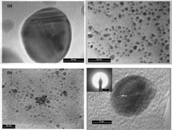
3.2.2 TEM images of (a) sample A, (b) sample B………...………..45
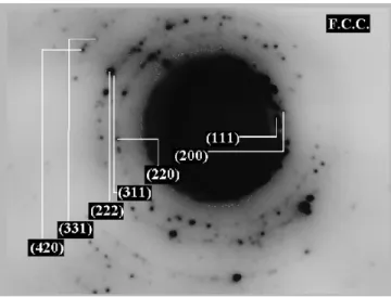
3.2.3 Typical SAED pattern of nanoparticles in ethanol………...…46
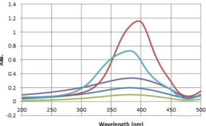
3.2.4 Surface plasmon resonance (SPR) from silver nanoparticle samples A (red) and B (blue)...………...47
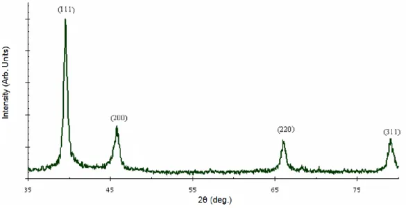
3.2.5 Typical XRD pattern recorded from a drop-coated film of Ag/polymer nanocomposite on a glass substrate…………...………....47
3.2.6 SPR absorption of sample A (blue), sample D (green)………...…...48
3.2.7 TEM images of sample D………...49
3.2.8 SPR absorption of silver/silver oxide nanoparticles (sample E) during 3 hours…..…...50
9
3.2.10 XRD from Silver chloride/ polyaniline (PANI) core–shell (sample F)………...51
3.2.11 FTIR spectrum of AgCl/PANI core–shell composite………...51
3.2.12 Final SPR peak absorption of gold nanoparticles………...53
3.3.1 Silicon substrates, (a) Thermally oxidized silicon wafer, (b) HMDS treated transistors...54
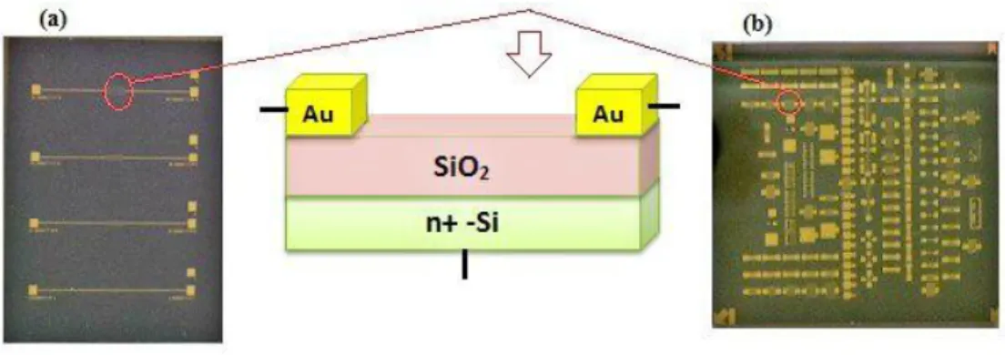
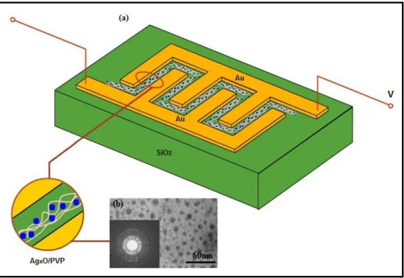
3.4.1 (a) Schematic diagram of PVP capped silver nanoparticles between interdigitated Au microelectrode arrays, fabricated on thermally oxidized silicon wafers, (b) TEM image and X-ray differaction of PVP capped silver nanoparticles...56
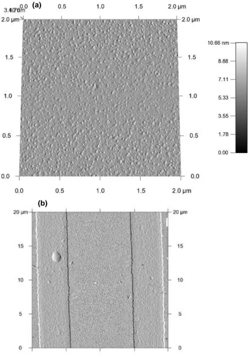
3.4.2 (a) Typical AFM image of PVP capped silver nanoparticles based diode type-B (b) Image of diode type-C (silver nanoparticles were prepared by electron beam evaporation), interdigitated Au microelectrode arrays, fabricated on thermally oxidized silicon wafers...57
3.4.3 (a) Typical AFM image of PVP capped silver nanoparticles based diode type-E (b) Typical AFM image of diode type-Au...58
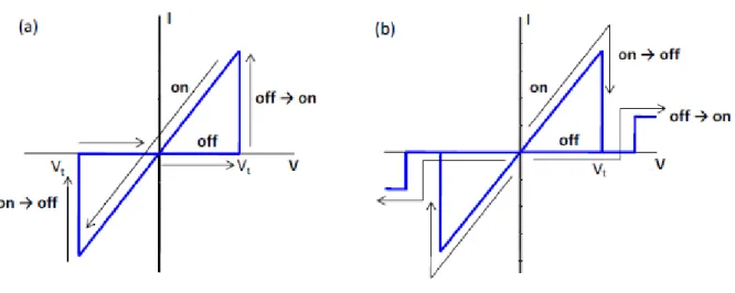
4.2.1 Schematic representation of N-shape I-V characteristics………...60
4.2.2 Schematic representation of (a) Symmetric, (b) Asymmetric S-shape I-V characteristics….…...61
4.2.1 I-V characteristics of a SiO2 substrate coated with a thin film of PVP. The resistance is approximately 0.5 TΩ under an applied voltage of 50 V. The measurement is done in vacuum...62
4.2.2 The I-V characteristics of AuNps in air………...63
4.2.3 The I-V characteristics of AgNps-PVP based device in air………...64
4.2.4 Current-voltage characteristics, (a) symmetric S-shape and (b) asymmetric, of silver oxide Nps-PVP (silver-PVP) planar diode (L: 10 µm)………....…...64
4.2.5 Retention time for both on and off states of a silver-PVP planar diode (L: 10 µm) in air…...65
4.2.6 Pristine-state and the final electroformed loop of silver-PVP planar diode (L: 10 µm) in vacuum...66
4.2.7 (a) I-V characteristics showing the on-state of silver-PVP planar diode (L: 10 µm) in vacuum...66
4.2.8 Endurance sweep cycles for a silver-PVP planar diode (L: 10 µm), in high vacuum (10-5 Torr): Write: 30 V, Erase: 50 V, and Read: 3 V. The on/off ratio is 4 orders of magnitude...67
4.2.9 Retention time for both on and off states of a silver-PVP planar diode (L: 10 µm) in high vacuum.67 4.3.1 Channel length dependence of the threshold voltage for switching from the off-state to the on-state for N- and S-shape switching...69
4.3.2 Current state at 3 V under N2/H2O gas exposure for a AgNps-PVP diode (L: 10 µm)...69
5.1.1 One-dimensional poly-walk: (a) in diffusion, the walk is directed by random scattering, (b) in percolation, the walk is controlled by the random medium...75
5.1.2 (a) As-fabricated state of the region (pristine-state), with the defects randomly distributed in an initial configuration (pink dots). (b) Percolation nanoscale filamentary path after the electroforming [97]...76
10
5.2.1 Current-voltage characteristics of a diode prior to electroforming. The hysteresis loops are typical of a capacitor like behaviour. The channel length L: 10 µm. The voltage ramp speed is 0.1Vs-1...77 5.2.2 Current-voltage characteristics of a diode during electroforming. The channel length (L) is 10 µm. The inset shows the Vforming for different channel lengths (L: 5 µm, 7.5 µm, 10 µm, 20 µm, 40 µm. (5
devices were measured for each L)...78 5.2.3 I-V characteristic of the on-state and off-state of a diode with silver nanoparticles, L: 10µm...79 5.2.4 The evolution of the current under a constant applied voltage (V=15 V) for a diode with L: 5µm...80 5.2.5 XRD patterns for the empty silicon oxide substrate (black), pristine state (blue), electroformed state (Red)...81 5.2.6 I-V characteristics of a diode fabricated with only a PVP layer. (a) Blue curve is the first measurement, the black curve is the second measurement. The dielectric breakdown occurs in the return path. The measurements were carried out in vacuum for a diode with a channel length of 5 µm...82 5.3.1 Schematic diagram of the three different types of filaments established upon electroforming. Permanent paths (bold green), programmable paths (narrow green) and paths that turn on and off intermittently or blink (in red). (a) During initial forming loops, (b) last forming loops (c) on-state, (d) off-state, (e) the lowest off-state...84 5.3.2 Schematic diagram showing the double barrier established between the silver oxide particle and the nearby polymer region. Oxygen vacancies in the oxide can trap holes and the oxygen rich nearby polymer regions trap electrons creating a local electric dipole...86 5.3.3 Schematic diagram of the compensating electron filamentary paths. This path is determined by the defect distribution and density...86 6.2.1 Symmetric current-voltage characteristics for different channel lengths (a) L: 5 µm, (b) L: 7.5 µm, (c) L: 10 µm. The on-state exhibits a pronounced NDR becomes more defined for higher channel lengths...92 6.2.2 I-V characteristics showing that as the applied voltage increases the NDR region is comprised of a cascade of switching-off events. Different off-states can be obtained by selecting the applied voltage...93 6.2.3 Different on- and off-states can be obtained by selective turning-off some of the current paths. This is done by applying voltages slightly above the NDR region, 35 V (black), 40 V (red), and 45 V (blue) for a time of 2 sec. (b) the programming of different conductance states can also be achieved by successively increasing the voltage range above the NDR region, In (b) is shown three different current states obtained by extending the scan voltage range, blue [0-60 V], red, black: [0-100 V] the ramp speed used is 500 mV/s...94 6.2.4 Time dependence of two on-states and 3 off-states. Different states can be programmed by controlling the amplitude and the time of the voltage step...94
11
6.2.5 Log (I)-Log (V) for both the on- and the off-state...95 6.3.1 Arrhenius plot for the on-, off- and the lower off-state. All plots are perfect parallel showing the same activation energy (72 meV). Channel length is L=10µm...96 6.4.1 Current fluctuations at the lower off-state...98 6.4.2 Typical time domain of the current fluctuation at NDR. The trace was recorded with an applied voltage of 40 V...98 6.4.3 Probability density function using the data in Fig. 6.4.2...99 6.5.1 Electrical characteristics of the on-state, voltage scan speed: 100 mV.s-1, 300 mV.s-1, 500 mV.s-1, 1000 mV.s-1 (L: 5 µm)...100 6.6.1 Temporal evolution of current from the off to the on-state after applying voltage steps of different magnitudes. The experiment started from high to low bias (L=10 µm)...101 6.6.2 Voltage dependence of the delay time for switching from off to on...102 6.7.1 Time response of the diode current to a few seconds light pulse. The diode is in the off-state with a constant applied voltage of 5 V...104 6.8.1 Hole flux, the same charge carriers at the on/off states, hole/electron recombination ruptures some conductive paths at the off-state...106 7.2.1 Schematic diagram of the device structure. The interdigitated gold microelectrode arrays were 10.000 m long (W), separated apart 10 m. The thin polymer film with the nanocrystals is approximately 1m thick. The substrate is a thermally oxidized silicon wafer with a 200 nm thick SiO2
layer...110 7.2.2 The pristine (blue) and the electroformed (black) states for AgCl nanocrystal polymer based diode, L = 10µm...111 7.2.3 The on/off I-V curves obtained after pulse at Von and Voff respectively for AgCl nanocrystal polymer
based diode, L = 10 µm...112
7.2.4 Initial current decay measured shortly after a programming pulse to the on-state. Inset shows the discrete variations in the current with a typical signature of random telegraph noise of AgCl nanocrystal polymer based diode...113 7.2.5 Endurance sweep of AgCl nanoclusters-PANI-PVP diode (L: 10µm), high vacuum: 10-5 Torr, Write: 18V, Erase: 30V and Read: 3V. The on/off ratio is 2 orders of magnitude...113 7.3.1 (a) Temperature dependence of the current-voltage characteristics of the AgCl nanocrystal polymer based device, below 245K the NDR disappears showing low conductance state, (b) Arrhenius plot of the high conductance state measured at 6 V. The line fits the experimental points (∆)...114
12
List of Tables
2.4.1 Summary of reported device characteristics...31 3.1.1 Total and surface number of atoms for FCC-structured silver nanoparticles together with an estimate of the particle size [54]………...40 3.2.2 Comparison of measured D-spacings for silver nanoclusters with D-spacings for FCC silver...46 4.3.1 Programming voltage process of N-shape characteristics for different channel lengths (L)...68 6.1.1 Charge transport mechanisms proposed in the literature for nanostructured resistive switching
13
CHAPTER 1- Motivations and Outline of the Thesis
In this chapter, a brief review in non-volatile memory developments is presented. The motivation of this research is also discussed. The thesis organization is presented at the end together with a list of publications of this work.
14 1.1 Motivations
There is a large demand for a high-density, high-speed, and low-power nonvolatile memory (NVM); the market of NVM has grown much faster than the entire semiconductor market in recent years [1]. Flash memory has been one of the most important key drivers of memory growth in terms of flexibility, cost and market size. However, as predicted by International Technology Roadmap for Semiconductors (ITRS) [2-3], the flash cell reduction will face physical limits in the near future due to the increasing difficulty of retaining electrons in shrinking dimensions. Flash also suffers from general shortcomings like slow programming (from microseconds up to milliseconds), limited endurance (typically 105-106 write/erase cycles) as well as the need for high voltages (10-20 V) during programming and erase. Therefore, new materials and novel device architectures are needed to overcome this technical and physical scaling limit.
There are various candidates competing for the next-generation memory. For example, magnetic random access memory (MRAM) and ferroelectric random access memory (FRAM), which use magnetic tunnel junctions and reversible polarization of ferroelectric materials, respectively, have attracted significant attention. However, both MRAM and FRAM face severe problems in scaling. Under this circumstance, a new candidate emerged: resistance switching random access memory (RRAM), in which the memory cells have the theoretically smallest area.
Resistive switching phenomenon was first reported in a series of binary oxides by Hickmott in 1962 [4]. Since then, the resistive switching behaviour under an applied electric field has been reported in many materials. Hence, the first period of research activity on resistive switching phenomena arose in the 1970s and 1980s. Most of the early research focused on discussing and revealing the physical mechanism of electrically stimulated resistive switching. Through the development of microelectronics processing technology, researchers recognized that resistive switching behaviour has the potential to be utilized as an ultimate NVM in the late 1990s, bringing the second research surge in resistive switching [5-12].
As shown in Fig.1.1, the number of papers on RRAM increased rapidly year by year [13],
indicating that this area is attracting enormous scientific interest because of the excellent scaling prospects and the outstanding operating and processing properties.
15
Fig. 1.1 Number of papers on resistive switching per year [13].
RRAM is still less mature than other emerging memory concepts, but it is appealing in its vast potential for exploiting a memory combining high density, high speed and non-volatility. In order to promote the commercial application of RRAM, further studies are required to elucidate the microscopic mechanism of resistive switching. Studies on reliability become important. What is the reason for cycling failure? How to improve retention time? How to improve yield and parameter dispersion? These unsolved issues and the coexistence of the scaling potential mean research in resistive switching can become a sustaining hotspot in fields of physics and electronics as well as in materials research.
The need for a deeper understanding of the physics of the resistive switching mechanism has been the major motivation for the work in this thesis. Towards this goal, we followed a twofold strategy: Firstly we use planar device structures. Although these structures are not useful for practical applications they offer an interesting research tool because they allow a decoupling of the effects related to electrodes from the effect relating to the bulk layers making the data analysis simpler. Secondly, in each sample we perform a systematic electrical characterization including temperature dependent measurements and dynamic measurements to study the time dependences of the physical process involved during switching. Our ultimate goal was to understand the basic processes that can control the change in resistance upon a voltage step. To gain further understanding we also compare the behaviour of our nanoparticle based device with
16
oxide-based memories and polymer or organic based memories. Apparently different devices show a common behaviour. This strong resemblance has been overlooked due to a lack of interaction between different scientific communities.
1.2 Outline of the Thesis
This thesis is organized into 8 chapters. Following this chapter, which gives an overview of the thesis, motivation and organization, the remainder of the thesis is arranged as follows:
Chapter 2 provides an overview of emerging memory technologies, followed by a review of the current status of nanoparticle memory based devices. The unsolved issues of RRAM in terms of the requirements for the future storage class memory will be also presented. This chapter concludes with the advantages and disadvantages of using planar devices when compared with more conventional sandwich structures.
In chapter 3, the fabrication methods and synthesis of metal nanoparticles (silver, silver oxide, gold, silver chloride) are explained. Different deposition methods are also presented. Thin films of metal nanoparticles were deposited on the silicon substrates by drop casting and spin coating. Structural and morphological characterization was done using TEM, UV-Vis spectroscopy, AFM and XRD.
Chapter 4 is concerned with a systematic investigation on the electrical properties of metal nanoparticles (silver and gold) in different ambient atmospheres. The same device structure can show different types of current-voltage (I-V) characteristics (S- and N-shape) depending on the surrounding atmosphere. The retention time and endurance cycles are also shown in this chapter. Chapter 5 mainly focuses on the electroforming process. The electroforming is presented as a dielectric soft-breakdown mechanism. In this chapter a model based on percolation networks is proposed to explain how conducting filaments can be formed in a nanostructured memory device.
In chapter 6, the study of the dynamic behaviour shows that repeated writing and erasing cycles require a time scale of seconds. It is proposed that this slow switching dynamic is related to the underlying physical process and if imposes a fundamental limitation on switching speed.
17
Electrical noise is also presented and discussed in terms of creation and annihilation of filamentary current paths. The weak temperature dependence of the current in all the conductance states is pointed to as evidence for a tunnelling charge transport mechanism. The overall electrical behaviour is tentatively explained in the light of a proposed resistive switching model.
In chapter 7, device characteristics of silver chloride embedded in a blend polymer (PANI and PVP) are presented. The current-voltage (I-V) characteristics consist of electroforming and on- and off-states will be shown. In this chapter, the temperature dependence of the on-state will also be presented. The data is discussed in the light of the previously developed model for charge transport mechanism in the silver nanoparticle based device.
Chapter 8 draws the major conclusions of this research and provides suggestions for future research in the area.
1.3 Peer Reviewed Published Work and Conference Presentations
Journal Publications
1. A. Kiazadeh, H. L. Gomes, P. R. F. Rocha, Q. Chen, A. M. Rosa da Costa, J. A. Moreira, D. M. de Leeuw and S. C. J. Meskers. “Intrinsic and extrinsic resistive switching in a planar diode based on silver oxide nanoparticles”, Thin Solid Films, 522, 407-411 (2012).
2. A. Kiazadeh, H. L. Gomes, A. M. Rosa da Costa, J. A. Moreira, D. M. de Leeuw, S. C. J. Meskers. “Non-volatile memory device using a polymer modified nanocrystal.”,Materials Science and Engineering B. 176 (19), 1552-1555 (2011)
3. A. Kiazadeh, H. L. Gomes, A. M. Rosa da Costa, J. A. Moreira, D. M. de Leeuw, S. C. J. Meskers. “Memristor based on silver oxide-polymer nanostructured thin film.” J. Appl. Phys. (pending).
4. A. Kiazadeh , Henrique Gomes, book chapter: Organic memory (molecular, hybrid and polymer memory), Woodhead publishing- Stanford University, Book: Advances in non-volatile memory and storage technology (accepted and under process)
Other related Journal publications
5. Paulo R. F. Rocha, A. Kiazadeh, Dago M. de Leeuw and Stefan C. J. Meskers, H. L. Gomes, “The role of internal structure in the anomalous switching dynamics of metal oxide/polymer resistive random access memories” J. Appl. Phys. 113 (13), 134504-134504-6 (2013)
18
6. H. L. Gomes, P. R. F. Rocha, A. Kiazadeh, D. M. De Leeuw and S. C. J. Meskers “Anomalous temperature dependence of the current in a metal-oxide-polymer resistive switching diode, J. Phys. D: Apply Phys. 44 (2), 025103 (2010)
7. Paulo R. F. Rocha, H. L. Gomes, Q. Chen, A. Kiazadeh, Dago M. de Leeuw and Stefan C. J. Meskers, Low-Frequency Diffusion Noise in Resistive-Switching Memories Based on Metal– Oxide Polymer Structure”, IEEE TRANSACTIONS ON ELECTRON DEVICES 59 (9), 2483-2487 (2012)
8. Q. Chen, H. L. Gomes, Paulo R. F. Rocha, A. Kiazadeh, Dago M. de Leeuw and Stefan C. J. Meskers, “Opto-electronic characterization of electron traps upon forming polymer oxide memory diodes”, Appl. Phys. Lett. 99, 083305 (2011)
Conference proceedings
9. A. Kiazadeh, P. Rocha, Q. Chen, H. L. Gomes, A. da Costa, J. A. Moreira: “New electronic memory device concepts based on metal oxide-polymer nanostructures planar diodes”, Technological Innovation for Value Creation: IFIP Advances in Information and Communication Technology Vol. 372, 521-526 (2012)
10. A. Kiazadeh, H. L. Gomes, Paulo R. F. Rocha, Q. Chen, A. M. Rosa da Costa, José A. Moreira, Dago M. de Leeuw and Stefan C. J. Meskers. “Planar non-volatile memory based on nanoparticles”, MRS Online Proceedings Library, part of Cambridge Journals (2011)
11. A. Kiazadeh, P. Rocha, Q. Chen, H. L. Gomes, A. da Costa, J. A. Moreira: “Resistive Random Access Memories (RRAMs) Based on Metal Nanoparticles”, TECHNOLOGICAL INNOVATION FOR SUSTAINABILITY Book Series: IFIP Advances in Information and Communication Technology Vol. 349, 591-595 (2011)
Oral and poster communications
1. A. Kiazadeh, H. L. Gomes, P. R. F. Rocha, Q. Chen, A. M. Rosa da Costa, J. A. Moreira, D. M. de Leeuw and S. C. J. Meskers. “ Resistive switching in nanostructured thin films”, Workshop NANO12, 21 October 2012, Lisbon, Portugal (oral communication)
2. A. Kiazadeh, H. L. Gomes, P. R. F. Rocha, Q. Chen, A. M. Rosa da Costa, J. A. Moreira, D. M. de Leeuw and S. C. J. Meskers. “Electrical behaviour of metal nanoparticles capped in PVP as insulating polymer” , 6th International Conference on Surfaces, Coatings and Nanostructured Materials (NANOSMAT-6), 19-21 October 2011, Krakow, Poland (oral communication)
3. A. Kiazadeh, H. L. Gomes, P. R. F. Rocha, Q. Chen, A. M. Rosa da Costa, J. A. Moreira, D. M. de Leeuw and S. C. J. Meskers. “Planar non-volatile memory based on nanoparticles”, 6th International Conference on Surfaces, Coatings and Nanostructured Materials (MRS spring meeting 2011), 25-29 April 2011, San Francisco , California, USA (oral communication)
19
4. A. Kiazadeh, Gomes H. L. and Tadjarodi A, ”Switching and Charge trapping phenomena in silver nanoparticles capped in polymers”, 6th
International Conference on Nanosciences & Nanotechnologies (NN9) 11-14 July 2009, Thessaloniki, Greece (poster presentation).
5. A. Kiazadeh, H. L. Gomes, A. R. Da Costa, J. A. Moreira, D. M. De Leeuw and S. C.J. Meskers, “non-volatile organic memory using a polymer modified nanoparticle device”, 7th
International Conference on Nanosciences & Nanotechnologies (NN10) 11-14 July 2010, Ouranopolise, Greece (oral Communication)
6. A. Kiazadeh, H. L. Gomes, A. R. Da Costa, J. A. Moreira, D. M. De Leeuw and S. C. J. Meskers, “Planar memory device based on silver nanoparticles”, 5th International Conference on Surfaces, Coatings and Nanostructured Materials (NANOSMAT-5), 19-21 October 2010, Reims, France (oral communication)
7. A. Kiazadeh, H. L. Gomes, A. R. Da Costa, J. A. Moreira, D. M. De Leeuw and S. C.J. Meskers, “Electronic memory devices based on metal nanoparticles”, MPA-4, 28-30 July 2010, Braga , Portugal (poster presentation)
8. A. Kiazadeh, H. L. Gomes, P. R. F. Rocha, Q. Chen, A. M. Rosa da Costa, J. A. Moreira, D. M. de Leeuw and S. C. J. Meskers. “New Electronic Memory Device Concepts Based on Metal oxide-polymer nanostructured planar diode”, DOCEIS 2012, 27-29 Feb. Caparica, Lisbon, Portugal. (oral communication)
9. A. Kiazadeh, H. L. Gomes, P. R. F. Rocha, Q. Chen, A. M. Rosa da Costa, J. A. Moreira, D. M. de Leeuw and S. C. J. Meskers. “New Electronic Memory Device Concepts Based on Metal oxide-polymer nanostructured planar diode”, DOCEIS 2011, Feb. Lisbon, Portugal. (oral communication)
20
“The world little knows how many of the thoughts and theories which have passed through the mind of a scientific investigator, have been crushed in silence and secrecy by his own severe criticism and adverse examination.” Michael Faraday
CHAPTER 2 - Overview of emerging memory technologies and review of the
current status of nanoparticle memory based devices
This chapter presents a summary of current understanding of resistive switching materials and devices. An introduction is given to the motivations behind the use of nanoparticle-polymer based resistive memory. Some basic concepts about memories are introduced along with a discussion of the current major memory technologies and their limitations.
Comparisons between the different classes of memory devices that have been investigated by others will then be given, describing the general structure of the devices and the characteristics they exhibit.
21 2.1 Introduction: Non-Volatile Memory
Generally, semiconductor memories can be divided into two categories, the volatile and the nonvolatile memories. Volatile memories are fast in writing and reading and can be integrated in very high density (dynamic random access memory (DRAM)) but once the power supply is turned off the data stored will be lost. In contrast, nonvolatile memories can keep the data without a power supply (hard disc drives (HDD) and flash memories). The name “flash” was given to emphasize the phenomenon that the whole memory array can be erased “in a flash”, meaning a very short time.
The increasing adoption of electronic low-volume portable devices with low power consumption and high performance capacity is pushing up the demand for non-volatile memories (NVMs). Smart phones, music players and tablets are only a few examples of the ever increasing role played by NVM in changing our life style. From a simple concept in the early 80’s, Flash memory, the actual market leader of NVMs, grew up and generated close to $23 billion in worldwide revenue in 2007 [14], representing one of the many success stories in the semiconductor industry.
This incredible growth was essentially driven by Moore’s Law, which led to dramatic reductions in unit cost over the past few decades for the entire semiconductor industry. This enables NVM to fulfill the requirement for products of ever higher density while continuously pulling down market prices.
As can be seen in Fig. 2.1.1, the cost of flash memories has fallen from $10 000 per gigabyte in the mid 90’s, to approaching $1 per gigabyte in 2010 [15]. This continuous reduction of the memory price enabled the creation of new markets that in turn largely repaid the efforts devoted to the manufacture of memory chips with increased performance and functionalities. All these improvements were made possible by the innovation in the industry along different fronts, firstly, in lithography which is fundamental for the area scaling. Great contribution were also provided by innovative self-aligned technologies, the introduction of NAND1 memories to reduce memory cell size, the introduction of multi-level cell technology and wafer size increasing from 150 mm in 1987 to 300 mm in recent years [14].
1
NAND flash memory architectures: small blocks of cells are connected in series between a high input signal and ground.
22
Fig. 2.1.1 Cost per GigaByte (GB) of Desktop and Enterprise hard disk drives (HDD) compared to the cost reduction trend in DRAM and NAND flash memory [15].
Despite their high cost per bit with respect to magnetic hard disk drives, semiconductor memories became the winning solution in all the consumer products requiring light weight, low size, low power consumption and high reliability. Fig. 2.1.2 reports the significant developments in NAND flash memory over the past few years, as extracted from the works presented at the International Solid-State Circuits Conference (ISSCC 2011). Continuous scaling down of the memory cell has resulted in an exponential increase of the memory density per chip.
Fig. 2.1.2 Observed trend in flash memory capacities in the past 12 years, presented at ISSCC (data from ISSCC 2011 documentation).
23
Note that in 2010, the reduction in process feature sizes, coupled with advanced multi-level cell (MLC) techniques have yielded a 32 Gb/chip capacity in a 32 nm technology with 2 bit/cell operation.
However, in order to guarantee an ever increasing memory density and ever decreasing memory costs, something more than the mere scaling down of feature size will be necessary, due to the intrinsic physical limits that flash technology will face in the next years [3]. As an example of some of these problems, we can cite the presence of oxide traps, contributing threshold-voltage instability issues such as stress-induced leakage current (SILC) [16], and cell-cell electrostatic coupling in the array [17]. A basic scheme of the flash memory is depicted in Fig. 2.1.3. Flash memories essentially consist of a metal oxide semiconductor field effect transistor (MOSFET) which is a transistor with tunable threshold voltage. As in a conventional transistor, the structure presents a floating gate (FG), in which it is possible to store charge, typically electrons.
Fig. 2.1.3 Schematic view of a flash memory cell: the charge is stored in the floating gate (FG) by applying the proper voltage to the control gate (CG); tunnel and control dielectric are also shown.
In terms of memory applications, it is generally believed that transistor based flash memories will approach the end of scaling within about a decade. Hence, one of the most important challenges in semiconductor industry is the need for a new memory technology which combines the best features of current memories such as high density of DRAM, fast speed of SRAM and the nonvolatile properties of flash with a CMOS compatible fabrication technology.
24
As a result, novel, non-FET based devices and architectures, which do not suffer from the same problems associated with transistor scaling, will be needed to meet the demands for devices of high density and high performance. Several nonvolatile memory device structures such as Ferroelectric random access memory (FeRAM), Magneto-resistive RAM (MRAM), Resistive RAM (RRAM) and Phase Change RAM (PCRAM) have been proposed. These emerging memory devices can store information and switch into different states (e.g. ‘0’ and ‘1’) by several mechanisms such as: ferroelectrification of a dielectric layer in a capacitor, which affects stored charges in the capacitor [18]; switching of magnetization in ferro-magnetic layers [19]; conducting path formation in organic materials [4] and phase change of a material from an amorphous state to a crystalline state [20]. The states of memory devices can then be distinguished by sensing the current flow through the devices in specific conditions, which reflects the state (stored information) of the memory. Unfortunately, none of the approaches seem ideal. For example, even though FeRAM and MRAM possess fast switching (< 20ns) and large programming endurance (> 1014 write/erase), these devices are not CMOS compatible. For PCRAM, the resistance switching involves Joule heating, which inherently imposes power consumption issues. Furthermore, the phase change is a volume effect which poses questions of whether the phase change can be uniformly controlled in ultimately scaled-down devices in which surface to volume ratio is very high.
The work reported in this thesis is focused on RRAMs based in a polymer matrix with embedded nanoparticles. After this introduction, the chapter presents resistive switching phenomenon and its possible use in resistive random access memories (RRAMs). The mathematical model to explain the resistive switching known as the Memristor is also introduced. Finally a review of nanostructured polymer based memory devices is presented.
2.2 RRAM- Resistive Random Access Memory
Resistive switching refers to the physical phenomenon of a dielectric suddenly changing its (two terminal) resistance under the action of a strong electric field or current. The change of resistance is non-volatile and reversible. Typical resistive switching systems are capacitor-like devices, where the electrode is an ordinary metal and the dielectric a transition metal oxide
25
(TMO). The basic characteristic of RRAM is its two different resistance states, i.e. high resistance state (HRS) and low resistance state (LRS), which can be switched from one to the other by an appropriate electric stimulus.
RRAM architectures potentially offer the simplest cell structure of all the emerging memory technologies, with a simple crossbar structure of electrodes on either side of a switching medium. Fig. 2.2.1 shows a two-terminal RRAM device. The resistance of the switching medium can be modulated by applying an electrical signal (current or voltage) to the electrodes. Even though large electrical nonvolatile resistance changes are also observed in FeRAM, MRAM and PRAM, the term RRAM typically refers to memory devices in which ferroelectricity, magnetization and phase change of material states (i.e. amorphous to crystalline) are not involved, hence distinguishing RRAM from FERAM, MRAM and PRAM.
Fig. 2.2.1 Two terminal RRAM structure. The resistance of the switching medium determines the state of the device.
The resistance switching effect has been observed in a broad range of materials such as organic materials [4-7], perovskite oxides [21] and transition metal oxides [22, 23] and currently, an organic layer consists of deliberately introduced nanoparticles [11]. In many of these materials, resistive switching was observed after an electroforming process. The electroforming is performed by application of a high voltage. The voltage is terminated when the current reaches the predetermined compliance level. The electroforming is often related to the soft breakdown of these materials (see chapter 5).
26
In general, resistance switching can be classified into two types, bipolar (or S-shape) and unipolar behaviour (or N-shaped).
In bipolar switching, the switching medium changes its resistance depending on the polarity and magnitude of the applied signal. For example, the device can be changed into an on-state (LRS) when a positive voltage larger than the threshold voltage (Vt) is applied to the top electrode, while a negative voltage larger than the threshold voltage switches the device back to the off-state (HRS). The operation which changes the resistance of the device from HRS to LRS is called a ‘SET’ process, while the opposite process is defined as ‘RESET’. Once RRAM is set to a specific state, the device can retain the information for a certain period without electrical power, which is termed the retention time.
Fig. 2.2.2 Two types of resistance switching. (a) bipolar switching (b) unipolar switching.
Because the resistance switching is observed in a broad range of materials, the exact switching mechanism is not a universal model yet. In the case of unipolar devices, switching only depends on the magnitude of the applied bias, there is a local maximum in the current at a threshold voltage (Vt) followed by a region of negative differential resistance (NDR). With voltage application at the top and bottom of NDR, the low and high resistances are obtained.
In this thesis, both resistive switching behaviours (S- and N-shape electrical characteristics) for the same device structure will be shown.
27
The resistance switching in RRAM can be nonvolatile (data storage > years) and fast (switching speed of a few 100 ns). In addition, its simple two-terminal structure suggests scaling of RRAM can reach beyond the transistor scaling limit, and allows for the fabrication of crossbar memory structures which offer high density, random access, and 3D stacking capabilities. As a result, RRAM is considered one of the most promising approaches for next generation memory technologies.
2.2.1 Memristor function to define RRAM
RRAMs based on resistive switches can all be supported by the theoretical framework known as the memristor. The existence of the memristor (contraction of the words “memory” and “resistor”) was predicted by Leon Chua in 1971 in the paper “Memristor-The Missing Circuit Element” [24].
According to the above cited paper, in circuit theory, there are four fundamental variables: the current, the voltage, the charge, and the flux. Therefore, there are six possible combinations to link each of the variables with another. The first relation (eq. 2.1) is derived from the physical definition of charge and current: the charge is the time integral of the current. The second relation (eq. 2.2) is given by Faraday's law of induction: the flux is the time integral of the voltage.
( ) ∫ ( ) (2.1) ( ) ∫ ( ) (2.2)
Three other relationships are given by the behaviour of the so-called "basic circuit elements": the resistor, the capacitor, and the inductor. The resistor puts in relation the voltage and the current: (2.3)
The capacitor links the charge and the voltage by the following relation: (2.4)
The inductor gives the relationship between the flux and the current: (2.5)
Chua presented the memristor as the fourth basic two-terminal circuit element, which would allow giving the missing relationship between the flux and the charge. This relationship could
28
not be realized with any passive RCL circuit. According to Chua's work, the fourth element should be a nonlinear resistor with a memory effect: the memristor, which would be described as follows:
(2.6)
The mathematical definition of a memristive device provides the framework for understanding the physical process involved in resistive switching. Generally, changes in the memristance depend upon the history of the device.
2.3 Literature review of nanoparticles based RRAM devices
The use of nanoparticles in RRAM devices originated in the work of Simmons and Verderber in 1967 [25]. They were one of the first to use an “electronic” model to explain resistive switching on gold/silicon-monoxide/aluminium (Au/SiO/Al) stacks. It was postulated that injected gold ions introduce a broad band of localized impurity levels within the normally forbidden band of the insulator. Charge carriers are assumed to transport by tunnelling through the insulator between adjacent sites within the impurity band: the carriers also can be trapped within the impurity band. The next progression in devices came from structures first proposed by researchers at the University of California [7, 26-28]. The device was a tri-layer structure of organic/metal-nanocluster/organic sandwiched between two aluminium electrodes (named as 3-layer organic bistable devices, 3L-OBDs). An organic semiconducting polymer, 2-amino-4, 5- imidazoledicarbonitrile (AIDCN), was used for the organic layers. The metal-nanocluster layer was formed by evaporating a thin metal layer in the presence of oxygen or AIDCN, forming discontinuous metal-nanoclusters. It was proposed that a charge could be stored at either side of the nanocluster layer, thereby doping the AIDCN layers and significantly increasing the conductivity of the device. Many permutations of metals [7] and various layer thicknesses [28] were studied with on/off ratios in the devices ranging from 4 – 6 orders of magnitude, depending upon the structure studied. He et al. [27] showed that switching mainly occurs in the bottom organic layer, postulating that this was due to the organometallic complex formed by evaporating the top contact, giving rise to an asymmetric device structure. The paper also shows devices can be made asymmetric by deliberately introducing an Al2O3 layer under the top electrode.
29
However, this casts doubt over the mechanisms discussed, as Al2O3 was one of the first materials reported to exhibit resistive switching. Subsequent reports by Tondelier et al. [29] studied the same structure as well as devices without the middle metal-nanocluster layer and found that a similar switching behaviour was present. They concluded that metal nanoparticles were included in the polymer layer due to the thermal evaporation of the top electrode, with metallic filaments of nanoparticles forming in the polymer under high electric fields, giving rise to a high conductivity on-state. A subsequent evolution in device structure came by including ready-made nanoparticles in the devices, rather than relying on nanoparticles forming during fabrication. Paul et al. [30] demonstrated the first of these devices by incorporating a monolayer of gold nanoparticles via the Langmuir-Blodgett technique into the insulating layer of metal-insulator-semiconductor (MIS) capacitors. Capacitors including nanoparticles were found to show hysteresis in their capacitance-voltage characteristics when compared to devices without nanoparticles. This was attributed to electrons being injected into the nanoparticles from the electrode, charging the nanoparticles and allowing data storage. Similar results were also demonstrated in MIS structures more recently by Leong et al. [31], however, they attributed the hysteresis as being due to holes injected into the nanoparticles. Although the devices described in these papers were not used directly as memory devices, they demonstrated that the principle of using nanoparticles as charge storage elements was feasible. The first paper to integrate discrete nanoparticles into MIM memory structures was presented by Ouyang et al. [8], who demonstrated resistive switching behaviour in devices comprised of an admixture of gold nanoparticles capped with dodecanethiol (termed Au-DT in the report). These nanoparticles are also the same as the Au nanoparticles/8-hydroxyquinoline (8HQ) molecules in a polystyrene matrix. It has been shown that 8HQ and gold nanoparticles can act as electron donors and acceptors respectively [32-34], with the change in conductivity in these devices attributed to the transfer of electrons. Ouyang et al. [35] later studied MIM structures including nanoparticles capped with 2-naphthalenethiol (Au-2NT) embedded in a polystyrene matrix. Here the proposed mechanism was a transfer of electrons from the capping ligands of the nanoparticles and the nanoparticle core itself, with tunnelling between the nanoparticles responsible for the conduction in the on-state. These devices were found not to have a transition back to the off-state. Work on investigating the effect of nanoparticles based on different metals, as well as their position in the structure and electrode material has been carried out by Bozano et al. [11-12]. Electrical
30
bistability was shown to be a common phenomenon among the materials chosen and the structures investigated. All devices used a semiconducting or insulating organic material as organic layer, with compositions similar to those studied in [7] and [8]. However, once again, Bozano et al. reported N-shaped I-V characteristics, in disagreement with those of Ma et al. [7] and Ouyang et al. [8-9, 35]. Bozano et al. found that characteristics were broadly similar to those reported by Simmons and Verderber (SV) [25] in their work on electroformed MIM structures and concluded that similar conduction mechanisms are responsible. The main difference was that, in the SV model, Au atoms introduced from the electrodes create charge transport and trapping sites in the insulator, whereas in Bozano’s device structures that role is played by the metal nanoparticles. Hence, conduction in the on-state is dominated by tunnelling between the nanoparticles. Devices based on gold nanoparticles and 8HQ admixtures have also been investigated by Prime et al. [36-37]. Interestingly, in these devices the electrical characteristics were reported with no abrupt transition between on- and off-states. Other structures based on gold nanoparticle charge transfer complexes have also been studied, with P3HT [38], and PVK [39] being used as both electron donor and polymeric matrix. Similar S-shaped characteristics were reported. Reddy et al. [40-41] found Poole-Frenkel emission to be dominant in the off-state in devices based on aluminium nanoparticles, while on-state current fitted Fowler-Nordheim tunnelling. In order to ensure nanoparticles were well dispersed in the devices, Tseng et al. [42] incorporated platinum nanoparticles into the tobacco mosaic virus (TMV), finding that bistability only occurred when the nanoparticles were present, with the mechanism again being attributed to charge transfer, this time between the TMV and the nanoparticles. Another memory structure demonstrated by Ma et al. included copper ions introduced into an AIDCN layer [43]. This device switched to a high conductivity state at approximately 0.7 V, and switched off again at 2 V. Ma et al. proposed that the electric field induced migration of the Cu+ ions into the polymer layer caused metallisation of the latter which resulted in a high conductivity state. At higher voltages, the ions drift all the way across the polymer layer, returning back to an insulator.
In the majority of the work published to date, bistability, on/off ratio, and non-volatility are reported, which constitute the absolute minimum requirements for a device to be called a memory. Other important device characteristics such as retention time and memory cycles before failure are either omitted completely or show large discrepancies. This lack of data regarding longer term memory performance could be a symptom of the general trend in the field to overly
31
concentrate on the on/off ratio of the devices, which have now reached extraordinary levels. A summary of reported data for the different characteristics is included in Table 2.3.1, with the data being limited only to devices containing metal and metal oxide nanoclusters or nanoparticles.
Table 2.3.1 Summary of reported device characteristics.
Characteristic Minimum reported Maximum reported on/off ratio 10 [12, 34-35] 109 [26]
Retention time > 3 hours [25] Several weeks [23-24] Memory cycles ~ 50 [34-35, 37] > 1 million [23-24]
Of these characteristics, the on/off ratio actually raises many questions regarding the working mechanisms. For example, it is an incredibly high current density for organic based materials with thicknesses of generally less than 100 nm and lateral dimensions of a few millimetres. Especially when considering ratios are as high as 109 which have on-state current at milliamps.
2.4 Requirements for the future storage class memory
Based on current flash characteristics, the requirements for a memory to be competitive in future are as follows: (Based on ITRS values):
The minimum feature that can be patterned with the lithography processes of the technology used < 22 nm.
Minimum resistive ratio 10.
Write/read speed <100 ns. (Flash > 10 µs) Write voltage 1 V to 5 V. (Flash > 5 V) Retention time: 10 years.
32
Therefore, future memories will have to be at least two orders of magnitude faster than flash and able to achieve a number of write cycles of at least 107. Those values are the reference for future comparison with our experiments, and to decide if a new technology can be competitive. Of course, the industrial production feasibility and price will also play a major role.
2.5 Unsolved issues
Despite continued research there is still much speculation over the exact mechanisms that are responsible for the large change in conductivity observed in resistive memories based on nanoparticles. The main hypotheses which have so far been reported are as follows:
Charge transfer creating an internal electric field. This internal electric field then either enhances or diminishes an external voltage applied to the device, thereby giving either high or low conductance.
Nanoparticle/nanocluster presence leading to a change in material properties. Based on charge trapping, various electrical conduction mechanisms have been proposed including space charge limited current, Poole-Frenkel emission, and Fowler-Nordheim or direct tunnelling.
Formation of current filamentary paths between electrodes. Conductive filaments are formed under electrical stress, either from migration of electrode material, alignment of nanoparticles or an oxygen vacancies chain. These filaments can then be ruptured, returning the device to a low conduction state.
Modelling of the resistive switching in each aforementioned assumption results in a failure: The trapping-detrapping of electronic charges faces an insolvable voltage-time dilemma.The large retention time of 10 years for nonvolatile memories calls for sufficient barriers to suppress the escape of the trapped electronic charge by thermally activated or tunnelling processes. At the postulated low voltages, these necessary barriers prevent high enough current densities needed for short read and write pulses (<100 ns) in the small areas (<10−10 cm−2) of ultrahigh integrated memories [44]. The stochastic nature of the thermal dissolution of the metallic filaments produces off-state voltage variations leading to non-reliable physical explanations. Moreover, the
33
metallic filamentary (or REDOX based) mechanism is not processing at low temperatures. Oxygen vacancy configuration is also generated by randomly placing a specified number of oxygen vacancies during the electroforming process, representing the weak spot of fabricated as such RRAM device.
Until the resistive switching mechanism is understood in greater detail, this is likely to prove a large obstacle in the development and possible commercialization of RRAM. In summary, there are several issues of missing or ambiguous data concerning RRAM that will each be investigated throughout the course of this research:
A study of the switching mechanisms in nanoparticle based RRAMs.
A study of the individual roles of each device component, insulating matrix, nanoparticle and electrodes in the resistive switching phenomena.
2.4. Conclusions
Actual memory technologies, such as flash type memories are approaching a scaling down limit beyond which they cannot be improved. There is a strong need for a new type of memory to meet the strong demand to store more information. A strong candidate is the resistive switching type of memory. This memory can be fabricated using metal nanoparticles embedded into a polymer insulating matrix. In spite of decades of research, the mechanism behind resistive switching remains elusive. This lack of knowledge is limiting the optimization and eventually the commercialization of these resistive RAMs.
34
“The universe is full of magical things patiently waiting for our wits to grow sharper.” Eden Phillpott
CHAPTER 3-Synthesis of metal nanoparticles and thin film deposition
This chapter describes the experimental methods used in this thesis to fabricate planar memory devices. These include, the synthesis of colloidal solutions of metal nanoparticles (silver, gold and silver oxide/chloride) and the deposition of thin films with embedded metal nanoparticles on the top of preformed microelectrode arrays on silicon substrates.
35 3.1 Introduction
The interesting properties of metal nanoparticles have been known for more than a century now, but the recent development in nano-fabrication techniques and lithography has expanded the interest to a wide range of applications over the last years. Among the different preparation methods, chemical synthesis of metallic nanoparticles is a simple and economical solution, which can be used on the large scale, necessary for industrial applications. In the present work, a novel approach to fabricate silver (Ag) nanoparticles will be described. Silver nanoparticles were synthesized by chemical reduction reactions. Silver nitrate was adopted as the main precursor, and reduced by N,N dimethylformamide (DMF) or ethanol (both are weak reducing agent) to produce particles of different size ranges. Particle size was measured by UV-Vis spectroscopy and transmission electron microscopy (TEM). TEM was used to inspect nanoparticle structure and morphology. The main purpose of the chemical syntheses is the deposition of the silver nanoparticles onto silicon substrates to investigate resistive switching. Different techniques for depositing the colloidal silver solutions were tested. This chapter aims to address the basic terminology related to nanoparticles and fabrication methods. Then synthesis of nanoparticles embedded in a polymer host matrix will be presented. Deposition methods will also be briefly described.
3.1 Fabrication methods
3.1.1 Terminology
Following the increased focus on nanotechnology and materials in the nano-sized area, many new terms have been brought into use. Below is a short list of the most frequently employed into expressions in this work. A nanoparticle has all three external dimensions in the nanometer range, e.g. between 1 and 100 nm. If not all dimensions are in the nanometer scale the material is often referred to as nanostructured or nanoscaled; e.g. composition of interrelated constituent parts in which one or more of those parts is a nanoscale region. A nanocrystal is a nanoscale solid formed with a periodic lattice of atoms, ions or molecules. A metal nanocluster has at least
36
one dimension between 1 and 12 nanometers and a narrow size distribution. Colloids are not to be mistaken for chemical solutions. While the latter contain completely dissolved particles with sizes typically below the nanometer scale, colloidal particles are still small enough to be dispersed uniformly and maintain a homogenous appearance but they are also large enough to scatter light and not dissolve. These particles are in a state of constant random movement called Brownian motion due to collisions with the surrounding medium. Repulsive electrostatic forces or steric effects keep the particles in suspension (British standard institution: PAS 71:2011).
3.1.2 Metal nanoparticles synthesis methods
1. Wet chemical synthesis
The "bottom-up" method of wet chemical nanoparticle preparation is based on the reduction of metal salts, electrochemical pathways or controlled decomposition of metastable organometallic compounds [45]. Chemical reduction methods to produce silver nanoparticles vary in the choice of the silver precursor, the reducing agent and their relative quantities and concentrations, temperature, mixing rate, duration of reaction, etc. By the use of different reagents and conditions for the synthesis, large variations in the particle shape, size and size distributions may be expected. As for the source of silver, several salts have shown to be applicable [46, 47] but silver nitrate is by far the most adopted. It has been shown that stronger reducing agents produce smaller nuclei in the "seed" [45]. However, it is possible to obtain comparable reaction rates and particle sizes by adjusting the reaction temperatures. This will however, lead to differences in the internal crystal structure and thus the degree of crystalinity [48]. The chemical synthesis method is utilized in this thesis.
2. Physical methods of nanoparticle deposition
![Fig. 1.1 Number of papers on resistive switching per year [13].](https://thumb-eu.123doks.com/thumbv2/123dok_br/18629160.910912/16.918.270.623.104.397/fig-number-papers-resistive-switching-year.webp)
![Fig. 3.1.2 Percentage of atoms located on the surface of a spherical silver particle as a function of the diameter of the particle [54]](https://thumb-eu.123doks.com/thumbv2/123dok_br/18629160.910912/40.918.231.666.714.955/percentage-located-surface-spherical-particle-function-diameter-particle.webp)