The implemented active filter is of gm-C type and includes a current-controlled oscillator to support the realization of the above.
System Overview
- Superheterodyne
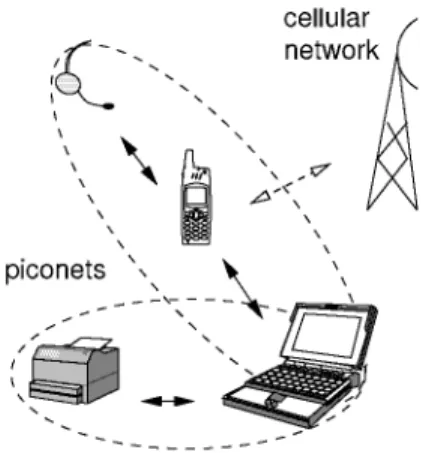
Although most portable devices at the birth of the Bluetooth project were already equipped with infrared links (IrDA). To comply with out-of-band government regulations, two guard bands are used: one at 2 MHz at the lower band edge and one at. The key concept behind this architecture is the use of the heterodyne principle to convert the incoming signal.
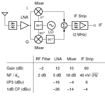
Since the two signals are no longer distinguishable at the output of the mixer, the unwanted of the two signals, called image, must be suppressed before mixing. The purpose of the preselection filters is therefore not only to suppress strong out-of-band signals which could saturate the front-end of the receiver, but also to suppress the image signal located at a frequency of 2fjp other than the desired one. The IK strip also provides most of the receiver gain, including, if necessary, an automatic gain control (AGC) loop.
In order to accommodate standards with different bandwidths, a variety of selectable channel filters are required. Doing so increases the noise figure of the receiver by at least 3 dB.
LNA |°° LO
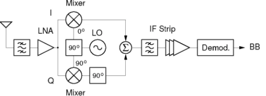
Direct Conversion
Over the last decade, the direct conversion receiver architecture has received a lot of attention because it is the architecture with the potential. The most serious problem faced by direct conversion receivers is the DC offset problem that requires the receiver to distinguish between the low-frequency components of the signal, which ideally extend into depth.
Direct Conversion
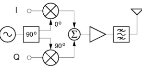
Flicker noise, which can be orders of magnitude larger than thermal noise, can be an additional factor limiting achievable sensitivity, especially in CMOS implementations. Here, any phase Si and gain SG mismatch between the two baseband strips gives rise to leakage of power from one sideband to the other, resulting in modulation distortion. Still, the DC offset should be minimized as it gives rise to LO feedthrough overlapping with the modulated carrier.
In medium and high power transmitters, the modulated output of the power amplifier (PA) can interfere with the LO signal [)<].
Open Loop Modulation
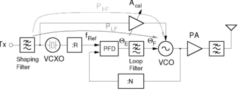
One possible solution to this problem is to open the synthesizer loop during the modulation intervals and "flywheel" modulate the VCO.
Two Point Modulation
The transfer function that describes the instantaneous VCO angular frequency io0 when the modulating signal Vfm is applied to the VCO input (path Phf in Figure 3.7) is. In addition, to satisfy equation (3.10), the gain of the VCXO or the gain of the VCO must be calibrated. Often, in a transceiver, the reference frequency of the PLL is also used as the base clock frequency of the baseband processor.
The effect of the slight frequency change introduced by the two-point modulator on the operation of the latter must therefore be taken into account. Since a fractional-N PLL allows a very fine control of the frequency, the modulation information can directly. The main disadvantage of this method is the fact that the compensation filter depends on the PLLloop filter.
Others must be translated into a metric appropriate to the design of the transceiver's front end. So after specifying the type of detector to use, the noise figure can be used as a better measure of the receiver front end.
Receiver Specifications
Selectivity and 1 dB compression point (CPidB) for each block of the system can only be specified once its IF frequency and range are specified.
Transmitter Specifications
The Receiver
The resistance of all other interfaces can be chosen freely and is best chosen during circuit design. MOSFETs are actually voltage-controlled devices whose nonlinear characteristics are best specified by voltage levels. Selecting the frequency of the IF receiver requires a trade-off between power consumption and noise.
To somewhat relax the linearity requirements of the IF strip, and in particular of the channel filter, only 20 dB of gain has been allocated for it. Due to the low supply voltage of 1.8 V and the difficulty of implementing linear transconductors, the channel filter will be the block limiting the top end of the dynamic range. Due to process, temperature and supply voltage variations, the filter center frequency must be adjustable, with a tuning range of approximately ±20%.
The Transmitter
Any spurious signal emitted by the PA during the reception time windows actually becomes a receiver. This tendency limits the number of units that can be stacked and often precludes the use of Some important characteristics of the TSMC 0.18 /jm CMOS process used for this project are summarized in Table 5 1 .

V 0.18 ina
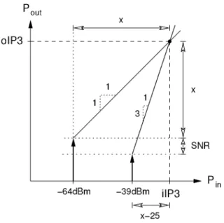
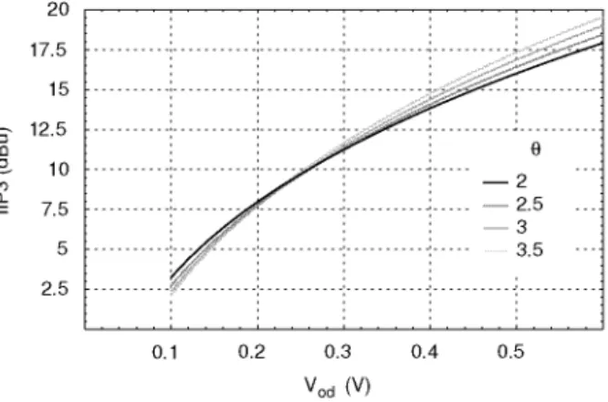
In particular, we calculate the third-order cutoff point referenced to the input of a common-source amplifier assuming that the I-V characteristic of the transistor is the dominant nonlinearity. At overload voltages lower than 0 V, the transistor is in weak inversion and its characteristics become exposed. As a result, iIP3 for vod < 100 mV degrades rapidly approaching the value—12.7+201og(n)dBu for negative values, where.
The inductor Ld is used to tune-out Cp and the parasitic drain-bulk capacitance of M2 so that only the real part of the load impedance needs to be considered for the design. Resistor Rd is used to lower the quality factor Qp of the load resonator and is set precisely. From (6.9) it also appears that the transconductance of the input stage Gm is set by Ls.
Simultaneously reducing the current and width of the transistor so that the transistor remains in strong in¬.
On Chip Rx/Tx Antenna Switch
Lg and its influence on the PA's output impedance can be easily corrected by fine-tuning Lm and Cm. An upper limit to the width of the transistors is set by their parasitic capacitances, most of which are proportional to the transistor width.

Image-Reject Mixer
- Single Balanced Mixer
Image-Reject Mixer 51
Image-Reject Mixer 53
The maximum size is thus limited only by the drive capacities of the stage drive.
C nMOS W (iiia) L (jum) Ida (mA)
- LO Phase Shifter
- Image-Reject Mixer 55
- Image-Reject Mixer 57
We analyze the phase error created by the second harmonic only, since the higher harmonics are always significant. The phase error a is amplitude and phase dependent: if the second harmonic component is in phase with. With a fully differential structure ESCL gates inject very little noise into the power supply and substrate and are immune.
The static power consumption in this logic family is not a problem here, as the divider always works at full speed. The predominant RC time constant that limits the speed of the circuit is provided by the load resistances and the total capacitive load.
- Image-Reject Mixer 59
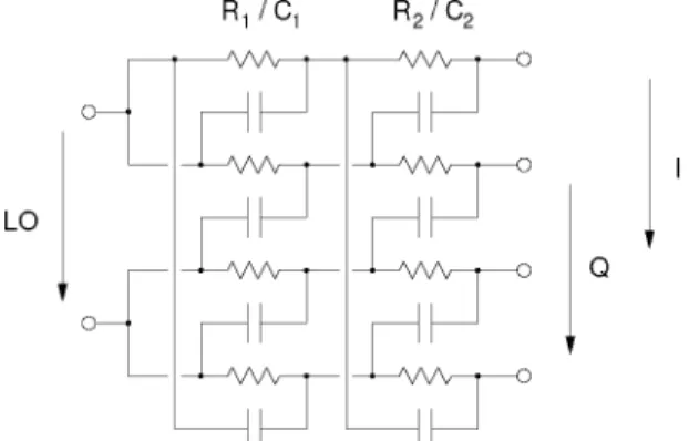
- IF Polyphase Filter
- Voltage Controlled Oscillator
- Measured Performance
- Linearized Transconductor
- Bandgap Reference
- Automatic Tuning
- Measured Performance
- IF Limiting Amplifier
- IF Limiting Amplifier 83
- Measured Performance
- Phase-Shift Network
- Multiplier
- Measured Performance
The common mode voltage of the filter is set with the help of the on-chip band reference. The first stage is connected to the rest of the amplifier with 12.5 pF coupling capacitors. The output currents of the differential pair are reflected in the switching transistors by the cur¬.
The circuit below the latter is a bandgap reference used to set the gyrator common-mode voltage. The block diagram of the prescaler is shown in Fig. 7 1 Just like the digital LO phase shifter is implemented in ESCLlogic Theprescaler.

12 To ensure a high production yield, the prescaler has been designed to work at a frequency 40% higher than required at nommai
- Measured Performance
- Measured Performance
- Crystal Oscillator 101
- Crystal Oscillator
- Crystal Oscillator 103
- Implemented Oscillators
- Crystal Oscillator 105
- Varactors
- Crystal Oscillator 107
- Amplitude Detector
- Crystal Oscillator 109
- Amplitude Dynamics
- Crystal Oscillator 111
- Crystal Oscillator 113
- Modulation Bandwidth of the VCXOs
- Measured Performance
- Crystal Oscillator 115
- kHz at 6 kHz, and triangular-like with Afpp = 1.78 kHz at
- kHz at 25 kHz. At this frequency the signal results strongly
- Crystal Oscillator 117