A High Eficiency Power Factor Correction Using
Interleaved Boost Converter With Fuzzy Logic
Control
M.BHUVANESWARIPG Scholar,
Department of Electrical and Electronics Engineering, Anna University, Regional Centre, Coimbatore,
Tamil Nadu -641047, India. [email protected].
R.SURESH KUMAR
Assistant Professor,
Department of Electrical and Electronics Engineering, Anna University, Regional Centre, Coimbatore,
Tamil Nadu -641047, India.
Abstract:
This paper presents interleaved front end boost converter to perform better power factor correction to store energy for electric vehicles. The interleaved boost converter increases reliability, decreased stress
on critical components, improves eficiency and more lexibility. The parallel connection of two boost
converters reduces the input ripple current of the converter. The interleaved boost converter with coupled inductors reduces the volume and copper usage of the magnetic components and also achieves high power
density. The coupled inductor delivers continuous current to improve the eficiency. The boost power factor correction (PFC) converter with auxiliary circuit optimizes the amount of reactive current during light load condition. In addition the control system regulates the amount of reactive current to guarantee zero voltage
switching (ZVS) during line cycle for different load conditions. The proposed interleaved boost converter
with coupled inductor was modeled and its performance is simulated and analyzed in Mat lab/Simulink
environment.
Keywords: AC/DC converter, Interleaved Boost Converter, Power Factor Correction (PFC), Zero-Voltage Switching (ZVS), Zero Current Switching (ZCS).
1. Introduction
Electric vehicle power conditioning system usually utilizes a high energy battery pack to store energy for the electric traction system. The high energy battery pack is typically charged from a utility ac outlet. PFC is essential to improve the quality of the input current which is drawn from the utility. Boost converters are generally used to realize input PFC and ac/dc conversion in the front end of an ac/dc converter.An interleaved boost converter usually combines more than two conventional topologies, and the current in the element of the interleaved boost converter is half of the conventional topology in the same power condition. The single boost converter can use the zero-voltage switching (ZVS) and/or ZCS to reduce the switching loss of the high-frequency switching [1]–[2]. The interleaved boost converters with ZCS or ZVS are proposed in [5].
International Journal of Engineering Science and Technology
e-ISSN : 0975-5462
switching through a simple passive auxiliary circuit which provide reactive current to charge and discharge the output capacitors of the boost MOSFETs and guarantee ZVS.
2. Interleaved Boost Converter
The proposed interleaved boost PFC converter with coupled inductor is shown ig 1.These topologies have higher eficiency than the conventional boost converter because the proposed circuits decrease the switching
losses of the main switches with ZVS.
T
Figure 1. Proposed interleaved boost converter
The converter can be designed to have a simple circuit, excellent current sharing characteristics, low input
current ripple and zero boost-rectiier reverse-recovery loss. Coupled inductor employed in the interleaved boost PFC converter also exhibits improved performance, such as increased eficiency, smaller size, and reduced EMI ilter.High switching frequency operation is necessary to achieve small size of the converter
3. Auxiliary Circuit
The proposed converter implements soft switching through a simple passive auxiliary circuit placed in between the two phases of the interleaved boost converter. Since there are no extra semiconductors used in the auxiliary
circuit, high eficiency and reliability are the main advantages of the proposed system.
Figure 2. Placement of auxiliary circuit in interleaved boost converter
The proposed converter is able to optimize the amount of reactive current required to implement soft switching based on the load condition and the input voltage. This auxiliary circuit is able to provide reactive current to charge and discharge the output capacitors of the boost MOSFETs and guarantee ZVS. The key limitations of the previously proposed auxiliary circuits for single-switch boost PFC converters are the use of extra semiconductor devices such as diodes and MOSFETs as well as passive components and the extra losses associated with the auxiliary circuit. The Proposed system reduces losses by using only inductors and capacitors.
4. Analysis of Boost PFC Converter
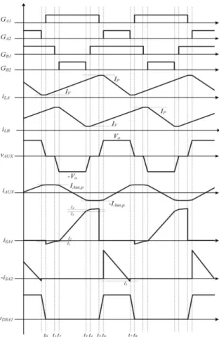
The waveforms of the converter for D >0.5 is shown in ig3. According to this igure, there are eight operating
Figure 3. Interleaved boost converter for duty ratio D>0.5
4.1. Operating Modes
Mode I (t0 < t < t1): This mode starts when the gate pulse is applied to Q1. Once the voltage is applied to the gate, Q1 is turned ON under zero voltage. Since Q1 and Q2 are ON during this interval, the voltage across the auxiliary inductor is zero. Thus, the current through the auxiliary circuit remains at IAux,p. Since the two phases have 1800phase shift, the value of t1 is given by
t1−t0=
(
D−0 5.)
Ts (1)The duty ratio is given by
D=
(
t1−t0)
fs+1
2 (2)
this mode ends once the gate voltage has been removed from Q2.
Mode II (t1 < t < t2): This mode is the dead time between the phase B MOSFETs. During this interval, the auxiliary circuit current charges the output capacitance of Q2 and discharges the output capacitance of Q4. In this mode, the average voltage across the boost inductance L1is zero. Therefore, the current through L1remains constant at its peak value.The voltage across the auxiliary inductor is given by
aux 1
( )
0(
)
2 1V
V t t t
t t
= − −
− (3)
International Journal of Engineering Science and Technology
e-ISSN : 0975-5462
This mode ends once the gate signal of Q4 has become zero.
Mode IV (t3 < t < t4): During this mode, the output capacitor of Q4 is charging from zero to Vo and the output
capacitor of Q2 is discharging from Vo to zero. This period is actually the dead time between Q4 and Q2 (t4 − t3
= td). This mode ends once the gate signal is applied to Q2
Mode V (t4 < t < t5): This mode start when the gate signal is applied to Q2.Once the gate has been applied, Q2 is turned ON under ZVS. The switch current during this mode is given by
Q1
( )
V Aux,p in 01 V
i t I I (t t )
L
= + − − (5)
Since Q1 and Q2 are ON during this period, the voltage across the auxiliary inductor is zero; hence, the auxiliary inductor current remains constant at its peak value, IAux, p.
This mode ends once the gate signal is removed from Q1. The value of iQ1at this time is given by
Q1
( )
V Aux,p ins 1
V
i
t
I
I
D
f L
=
+
−
(6)Mode VI (t5 < t < t6): During this mode, the output capacitor of Q1 is charging from zero to Vo and the output
capacitor ofQ3 is discharging from Vo to zero. This period is actually the dead time between Q1 and Q3 (t6 − t5
= td). In this period, the current through the boost inductor L1remains constant at its peak value.The auxiliary inductor current iAux is given by
Aux
( )
Aux,p 0 5 2d V
i t I (t t )
2t L
= − + − (7)
This mode ends once the output capacitors have completely been charged and discharged.
Mode VII (t6 < t < t7): During this mode, the voltage across the auxiliary circuit is Vo. During this mode, the MOSFET channel Q3 is conducting the current to the output. The current through the auxiliary circuit is given by
( )
0 0Aux Aux,p d 6
V V
i t I t (t t )
2L L
= − + + − (8)
This mode ends when Q3 reaches zero.
Mode VIII (t7 <t<t8): During this mode, the output capacitor of Q1 is discharging from Vo to zero and the output capacitor of Q3 is charging from zero to Vo. In this mode, the current through L1is at its minimum value and the excess current from the auxiliary circuit charges and discharges the output capacitors. This mode ends once the output capacitors have been charged.
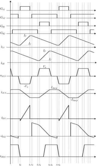
Figure 4. Interleaved boost converter for duty ratio D<0.5
The purpose of the power factor correction circuit is to minimize the input current waveform distortion and make it in phase with the voltage. The auxiliary circuit provides ZVS condition for the power MOSFETs when the
auxiliary circuit current decreases. In the proposed control system, the frequency is modiied once the duty ratio
has reached D=0.5.
Advantages of high power factor
• Reduce the distortion of voltage waveform.
• All the power is active, reactive power is negligible.
• The rms value of current is smaller.
• Number of loads that can be fed from the same source increases.
5. Simulink Model
The Simulink model of interleaved boost converter using Mat lab/ Simulink software is shown in ig 5. At
International Journal of Engineering Science and Technology
e-ISSN : 0975-5462
Figure 5. Simulation model of Interleaved boost converter
The frequency loop is introduced in the control system determines the frequency of the modulator based on the load condition and the duty cycle of the converter.
6. Simulink Result
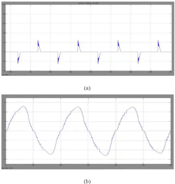
The experimental result for 3 kW is conducted to verify the performance of the proposed converter. The interleaved boost converter converts the rectiied input voltage to the intermediate dc-bus voltage. The output capacitor of the interleaved boost converter is large (1.4 mF) in order to decrease the 2nd harmonic voltage ripple caused by the power ripple of the input boost PFC converter. The simulation results of source current with and without power factor is presented. Due to power factor correction input ripple current is reduced. The experimental results are exported to Mat lab for plotting. They validate the effectiveness of the proposed control methods
(a)
(b)
Figure 6. Source current of interleaved boost converter (a) Without PFC correction (b) With PFC correction
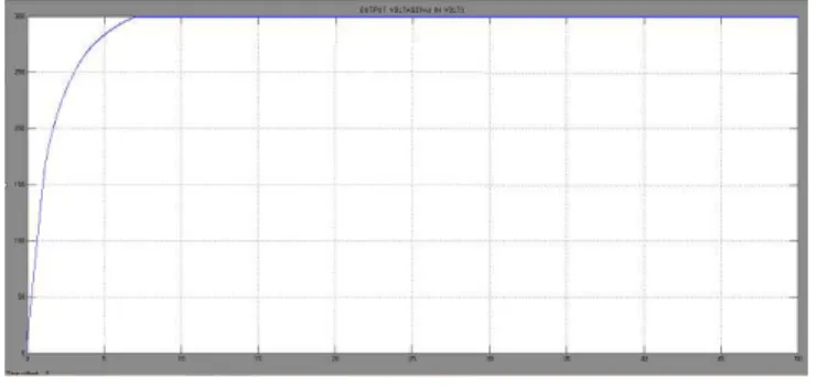
Figure 7. Output voltage
The waveform of source voltage and current of interleaved boost converter is shown in ig 8.The auxiliary circuit current is at its minimum at the zero crossing points of the input current and it is at its maximum at the peak of the input current. This implies that the auxiliary circuit current adaptively changes based on the shape of the input current and is optimized over the line cycle
Figure 8. Source voltage and current of interleaved boost converter
The boost MOSFET is turned on under zero voltage. This is due to the negative current provided by the auxiliary circuit. Basically, the output capacitor of the boost MOSFET is completely discharged prior to applying the gate signal and once the voltage across the MOSFET become zero; the gate signal is applied to the MOSFET.
.
Figure 9. Inductor current of interleaved boost converter
The simulation result of inductor current is shown in Fig9 . From this graph the switching losses and the turn on losses in the interleaved boost converter is reduced due to zero voltage switching.
7. Conclusion
International Journal of Engineering Science and Technology
e-ISSN : 0975-5462 References
[1] E. Adib and H. Farzanehfard, “Family of soft-switching PWM converters with current sharing in switches,” IEEE Trans. Power Electron., vol. 24, no. 4, pp. 979–985, Apr. 2009.
[2] C. A. Canesin and F. A. S. Goncalves, “A 2kW Interleaved ZCS-FM boost rectiier digitally controlled by FPGA device,” in Proc. IEEE Power Electron. Spec. Conf., Jul. 2006, vol. 2, pp. 1382–1387.
[3] C. M. de Olieira Stein, J. R. Pinheiro, and H. L. Hey, “A ZCT auxiliary commutation circuit for interleaved boost converters operat-ing in critical conduction mode,” IEEE Trans. Power Electron., vol. 17, no. 6, pp. 954– 962, Nov. 2002.
[4] H. Farzanehfard and S. Choi, “Zero-voltage-transition PWM converters with synchronous rectiier,” IEEE Trans. Power Electron., vol. 25, no. 1, pp. 105–110, Jan. 2010.
[5] Y.-C. Hsieh, T.-C. Hsueh and H.-C. Yen, “An interleaved boost converter with zero-voltage transition,” IEEE Trans. Power Elec-tron., vol. 24, no. 4, pp. 973–978, Apr. 2009.
[6] G. Hua, C.-S. Leu, Y. Jiang, and F. C. Y. Lee, “Novel zero-voltage transition PWM converters,” IEEE Trans. Power Electron., vol. 9, no. 2, pp. 213–219, Mar. 2004.
[7] W. Li and X. He, “ZVT interleaved boost converters for high-eficiency, high step-up DC–DC conversion,” IET Electron. Power Appl., vol. 1, no. 2, pp. 284–290, Mar. 2007.
[8] F. Musavi, W. Eberle, and W. G. Dunford, “A high performance single phase bridgeless interleaved PFC converter for plug-in hybrid electric vehicle battery chargers,” IEEE Trans. Ind. Appl., vol. 47, no. 4, pp. 1833– 1843, Jul./Aug. 2011.
[9] S. Park and S. Choi, “Soft-switched CCM boost converters with high voltage gain for high-power applications,” IEEE Trans. Power Electron., vol. 25, no. 5, pp. 1211–1217, May 2010.
[10] S.H. Park, S.R. Park, J.S. Yu, Y.C. Jung, and C.-Y. Won, “Analysis and design of a soft-switching boost converter with an HI-bridge auxiliary resonant circuit,” IEEE Trans. Power Electron., vol. 25, no. 8, pp. 2142– 2149, Aug. 2010.
[11] S. S. Saha, B. Majumdar, T. Halder, and S. K. Biswas, “New fully soft switched boost-converter with reduced conduction losses,” in Proc IEEE Int. Conf. Power Electron. Drives Syst., 2005, vol. 1, pp. 107–112.
[12] H.-Y. Tsai, T.-H. Hsia, and D. Chen, “A novel soft-switching bridgeless power factor correction circuit,” in Proc. Eur. Conf. Power Electron. Appl., Sep. 2007, pp. 1–10.
[13] C. M. Wang, “A new single-phase ZCS-PWM boost rectiier with high power factor and low conduction losses,” IEEE Trans. Ind. Electron., vol. 53, no. 2, pp. 500–510, Apr. 2006.
[14] G. Yao, A. Chen, and X. He, “Soft switching circuit for interleaved boost converters,” IEEE Trans. Power Electron., vol. 22, no. 1, pp. 80–86, Jan. 2007.