AN IMPROVED DESIGN FOR ZVT DC-DC PWM CONVERTERS
WITH SNUBBER ASSISTED AUXILIARY SWITCH
J. Russi, M. L. Martins, H. A. Gründling,
H. Pinheiro, J. R. Pinheiro and H. L. Hey
Power Electronics and Control Research Group - GEPOC Federal University of Santa Maria - UFSM
97105-900 - Santa Maria - RS – Brazil
[email protected], [email protected], [email protected] - www.ufsm.br/gepoc
ABSTRACT
This paper proposes an improved design to calculate the snubber auxiliary elements of ZVT DC-DC PWM converters with snubber assisted auxiliary switch. The proposed improved design guidelines are based on the reduction of the conduction losses through the auxiliary circuit. It is accomplished by the unique location of the turn-off snubber capacitor, which is shared by both active switches. By means of this improved design guidelines the converter efficiency can be increased.
An efficiency comparative analysis is carried out and the experimental results, obtained from 1 kW, 100 kHz laboratory prototypes, show a relevant improvement in converter efficiency compared to the original converter design. In addition, experimental results also confirm that with the improved design the ZVT PWM converters with snubber assisted auxiliary switch can be competitive with ZVT PWM converters with constant auxiliary voltage source (True PWM ZVS pole).
KEYWORDS: Soft-switching, ZVT, converters design.
RESUMO
Este artigo propõe uma metodologia de projeto aprimorada para determinação dos componentes auxiliares para o conversor ZVT CC-CC PWM snubber assisted auxiliary switch. O procedimento de projeto proposto é baseado na
redução das perdas de condução no circuito auxiliar. Isto é somente possível devido à localização do capacitor snubber de bloqueio, o qual é compartilhado por ambas as chaves ativas. Através do procedimento de projeto proposto o rendimento do conversor pode ser aumentado.
Uma análise comparativa do rendimento é apresentada e os resultados experimentais, obtidos de protótipos de laboratório de 1 kW, 100 kHz, mostram uma melhoria relevante em relação ao rendimento apresentado pelo projeto original. Além disso, os resultados experimentais também confirmam que o projeto proposto para o conversor ZVT snubber assisted auxiliary switch torna-o competitivo em relação ao conversor ZVT PWM com fonte auxiliar de tensão constante (true PWM ZVS pole).
PALAVRAS-CHAVE: Comutação suave, ZVT, projeto de conversores.
1 INTRODUCTION
With the aim of obtaining an improvement in overall performance of the PWM converters and further a reduction in size and weight of these power converters, soft-switching techniques have been the subject of intensive research. These techniques allow the power converters to operate with higher switching frequencies without penalizing the trade-off between switching losses and converter efficiency. Among these techniques, the commutation under Zero Voltage Transition – ZVT has been frequently employed, mainly when the active switches are implemented with majority carrier semiconductor devices. Besides the enhanced switching conditions for main devices, this technique also provides the absorption of main devices intrinsic capacitances. Moreover, the ZVT cell is placed in parallel with the main power path, enabling the converter to Artigo Submetido em 08/08/03
1a. Revisão em 27/09/04
operate as close as possible to its PWM counterpart, with low conduction losses when compared to other Zero Voltage Switching - ZVS techniques (Hua et al., 1995). In spite of ZVT converter proposed by (Hua et al., 1992) presents many advantages, its auxiliary circuit promotes inadequate commutation conditions to auxiliary switch. When auxiliary switch is implemented using power MOSFET devices, its output intrinsic capacitance enables Zero Voltage Switching - ZVS turn-off. Nevertheless, the energy stored during this process is totally dissipated when the switch is turned on reducing the efficiency gain of the soft switching approach (Erickson and Maksimovic, 2001). On the other hand, when IGBT devices are used, the turn-on capacitive losses are minimized but the turn-off losses associated with its current tail are not effectively reduced (Filho et al., 1994), which further limits its frequency operation.
Recently, several topologies have been proposed to minimize this inconvenient characteristic, which are based on one of the following principles:
a) Addition of a DC voltage source in series with the auxiliary switch Sa (Martins et al., 1993; Gegner and Lee,
1994; Gegner and Lee, 1994; Lee, et al., 1998; Filho, et al., 1994), yielding zero-current switching (ZCS) conditions to this switch. As ZCS switching conditions are well suited to IGBT devices the turn-on capacitive losses are quite reduced. Moreover, depending on the value of the DC voltage source, a reduction in reactive energy can be accomplished. Therefore, the conduction losses can be minimized. Nevertheless, the implementation of the auxiliary DC voltage source is done by means of (i) a voltage transformer (Martins et al., 1993; Gegner and Lee, 1994; Gegner and Lee, 1994; Lee, et al., 1998) or (ii) a converter voltage source or sink (Filho, et al., 1994), which can result in (i) demagnetizing problems and EMI degradation or (ii) operation under limited voltage ratio conversion;
b) Addition of a resonant circuit in series with the auxiliary switch also yields in ZCS conditions to this switch. Although low switching losses are achieved, the additional current stresses on main switch and/or additional voltage stresses on auxiliary switch (Yang and Lee, 1993; Moschopoulos et al., 1995; Tseng and Chen, 1998; Xu et al., 2000; Jain et al., 2001), resulting from the resonant tank operation, enlarge the converter conduction losses.
c) Addition of passive turn-off snubbers to the auxiliary switch (Streit and Tollik, 1991; Yaakov et al., 1995; Liu et al., 2000; Kim et al., 2000; Menegáz et al., 1999), which can effectively improve the switching conditions to auxiliary switch. However, they cannot avoid the turn-on capacitive losses due to parasitic capacitance present in auxiliary switch (MOSFET).
As it can be seen, none of the above mentioned solutions could enhance the ZVT features without adding some drawback. However, by the efficiency point of view, the reduction of reactive energy makes ZVT converters with auxiliary DC voltage source more attractive (Martins et al., 1993; Gegner and Lee, 1994; Gegner and Lee, 1994; Lee, et al., 1998; Filho, et al., 1994).
In spite of this fact, if the storage energy in both, main and auxiliary switch turn-off snubbers, is not discharged by the auxiliary inductor, instead of, being directly regenerated to the output, the conduction losses can be quite reduced. This way, ZVT converters with snubber assisted auxiliary switch can be as attractive as ZVT with auxiliary DC voltage source, without any inconvenient related to the DC voltage source implementation.
To accomplish these features, the ZVT DC-DC PWM converter with snubber assisted auxiliary switch presented in (Streit and Tollik, 1991; Yaakov et al., 1995; Liu et al., 2000), also referred as Flying Capacitor ZVT converter, was designed in such way that the auxiliary inductor and turn-off snubber capacitors for main and auxiliary switches are independent of each other, ensuring that there is no trade-off among the choice of their values. Therefore, they can be truly optimized, improving the converter efficiency performance.
This paper is organized as follows: Section 2 describes the ZVT PWM converters with snubber assisted auxiliary switch, as well as its operation principle. Section 3 presents an improved snubber design to calculate the snubber for the auxiliary switch. In Section 4 a comparative analysis between the original and the proposed design are carried out. Section 5 presents the comparative experimental results obtained from three ZVT PWM boost laboratory prototypes. Finally, Section 6 presents the conclusions from the analysis and the experimental results.
2 ZVT PWM CONVERTERS WITH
SNUBBER ASSISTED AUXILIARY
SWITCH - SAAS
The common DC-DC PWM switching cell, Fig. 1(a), can be used to derive every DC-DC PWM converter topology. Hence, to obtain a generalized analysis of the commutation process, this circuit, presented in (Zhu and Ding, 1999), is adopted. Assuming that the filter inductance L (L1) is large
enough, the current can be considered constant during one switching period of the PWM converter. Therefore, its circuit can be simplified as depicted in Fig. 1(b).
-Da1; two bypass diodes Da2 and Da3; a snubber inductor LS;
a snubber capacitor CSn; and the intrinsic switches output
capacitances CS and CSa. In steady-state operation the
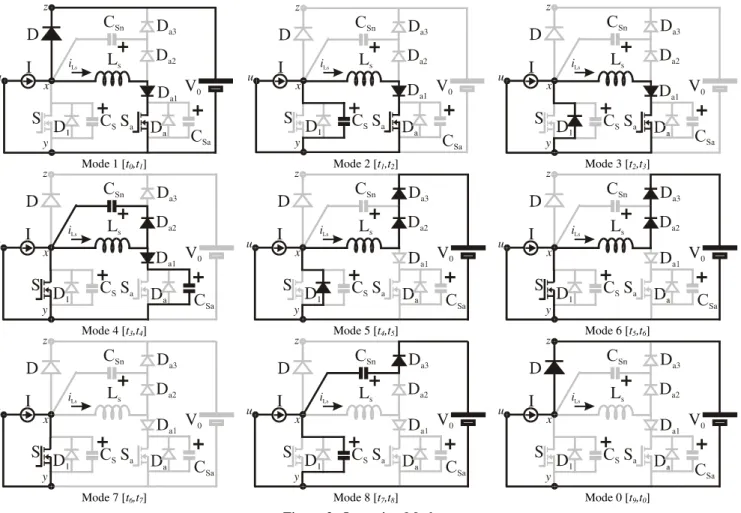
converter assumes nine circuit modes, Fig 3. The operation of each mode is described as follows.
Mode 0 (t<t0): Before t0, both switches are off and current I
flows through diode D. The converter PWM modulation defines the time for this mode. During this operation mode CSn is discharged and CS and CSa are charged to VZY.
Mode 1 (t0<t<t1): At t0 auxiliary switch Sa is turned on with
ZCS conditions and auxiliary inductor, currents ils increases
linearly with the following ratio.
Ls ZY S
i =V t L (1)
This mode ends when iLs reaches the value of current I.
1 0 S ZY
t − =t IL V (2)
Mode 2 (t1<t<t2): At t1 diode D turns off and the energy
stored in CS discharges through LS in a resonant way. The
resonant process is governed by the following expressions. L L1 x z y u u1 S (a) I I1 y S x z u u1 (b)
Figure 1. General PWM converter diagram. (a) Basic PWM switching cell; (b) Simplified PWM switching cell.
I
x zy u
iLs
L
sS
aV
0D
a2D
a3S
D
a1 I x z y uiLs Ls
Sa V0 Da2 Da3 S Da1
I
x z y uiLs
L
sS
aV
0D
a2D
a3S
D
a1Mode 1[t0,t1] Mode 2 [t1,t2] Mode 3 [t2,t3]
I
x zy u
iLs
L
sS
aV
0D
a2D
a3S
I
x z y uiLs
L
sS
aV
0D
a2D
a3S
I
x z y uiLs
L
sS
aV
0D
a2D
a3S
Mode 4 [t3,t4] Mode 5 [t4,t5] Mode 6 [t5,t6]
I
x zy u
iLs
L
sS
aV
0D
a2D
a3S
I
x z y uiLs
L
sS
aV
0D
a2D
a3S
I
x z y uiLs
L
sS
aV
0D
a2D
a3S
D
a1Mode 7 [t6,t7] Mode 8 [t7,t8] Mode 0 [t9,t0]
Figure 3. Operation Modes.
I
x z
y u
iLs
L
SS
aV
0D
a2D
a3S
D
a1( )
sin
Ls ZY S S
i = +I V ω t Z (3)
( )
cos
Cs ZY S
v =V ω t (4)
Where, ωS =1 L CS S and ZS = L CS S .
This mode lasts until CS to be completely discharged.
2 1 S S 2
t − =t π L C (5)
Mode 3 (t2<t<t3): At t2 main switch body-diode D1 turns
on. ZVS and ZCS conditions are ensured for main switch turn-on. This freewheeling interval should be as small as possible to minimize the auxiliary circuit conduction losses, however, it must last time enough to the gate source voltage signal turn S completely on.
Mode 4 (t3<t<t4): At t3 Sa is turned off, bypass diode Da2 is
turned on and iLs resonates with the equivalent parallel
capacitance comprised by CSn and CSa. As CSa<<CSn, the
dv/dt control is actually accomplished by CSn.
The resonant process is governed by the following expressions.
( )
3 cos( )
Ls Ls eq
i =i t ω t (6)
( )
3 sin( )
Csn eq Ls eq
v =Z i t ω t (7)
Where, ωeq=1 LS
(
CSn+CSa)
and Zeq= LS(
CSn+CSa)
.In this mode, current I is diverted to main switch. This mode lasts until vCsn reaches Vzy.
( )
(
)
1
4 3 sin ZY eq Ls 3 eq
t − =t − V Z i t ω (8)
Mode 5 (t4<t<t5): At t4 bypass diode Da3 turns on and
voltage across CSn and CSa is clamped at Vzy. In this mode iLs decreases linearly with the following ratio.
( )
3Ls Ls ZY S
i =i t −V t L (9)
This mode ends when main switch body-diode turns off.
( )
(
)
5 4 Ls 3 S ZY
t − =t i t −I L V (10)
Mode 6 (t5<t<t6): In this mode, iLs continues to decrease
linearly with the ratio defined by (9). This mode lasts until
iLs reaches zero.
6 5 S ZY
t − =t IL V (11)
Mode 7 (t6<t<t7): In this mode, current I flows through S
and converter operates as its PWM counterpart. The converter PWM modulation governs the duration of this mode.
Mode 8 (t7<t<t8): At t7 main switch is turned off and
voltage across its terminals increases linearly with the ratio defined below.
(
)
(
)
Cs Sn S
v = I C +C t (12)
As CS<<CSn, the dv/dt control is actually performed by CSn
This mode ends when vCs reaches VZY.
(
)
8 7 Sn S ZY
t − =t C +C V I (13)
Mode 9 (t8<t<t0): At t8, vCs reaches VZY and diode D turns
on. In this mode, current I flows through D.
The main theoretical waveforms are shown in Fig. 4.
3 IMPROVED SNUBBER DESIGN
In conventional design guidelines (Yaakov et al., 1995; Liu
et al., 2000), auxiliary elements LS and CS are defined as a
function of the current stresses on auxiliary switch, given by kI,
(
)
(
1)
I ZY S
k = + V Z I (14)
and the total ZVS time, given by tZVS,
i
Ls(t)
i
D(t)
i
S(t)
v
Cs(t)
V
zyV
zyV
zyv
Csa(t)
v
Csn(t)
S
S
at
t
t
t
t
t
t
t
t
0t
1t
2t
3t
4t
5t
6t
7t
8I
I
I
2
ZVS S ZY S S
t =IL V +π L C (15)
Solving (14) and (15) for LS and CS the following
expressions can be found,
(
)
(
1 1 2)
S ZY ZVS I
L =V t I +π k − (16)
(
)
2(
(
)
)
1 1 1 2
S ZVS I ZY I
C =It k − V +π k − (17)
Where kI is directly related to the conduction losses and are
chosen to be in a range between 1.3 and 1.5 times of current I and tZVS is related to the Minimum and maximum
duty-cycle. For DC-DC converter tZVS is in a range of 10% to
15% of converter operation period. On the other hand, in PFC applications it is significantly reduced to a range of 2% to 3% of the converter operation period.
The auxiliary capacitor CSn is chosen to assure the time
conditions given by tZVS or to ensure turn-off smoothness
for Sa.
The ZVT DC-DC PWM converter with SAAS has a unique characteristic that consist of the presence of a turn-off snubber CSn across the auxiliary inductor LS. By a proper
choice of CSn it can also smooth the main switch turn-off
commutation process. This way, main switch snubber capacitor can be as small as possible without penalizing the turn-off losses.
As the energy stored in CSn is regenerated to the output
without circulating through LS, CSn can be made large
enough to ensure low switching losses for both, main and auxiliary switch with no additional conduction losses. To ensure snubber operation for S and Sa, CSn must verify
the following expression.
(
)
(
)
2 2Sn S ZY S ZY
C ≤L I+ V Z V (18)
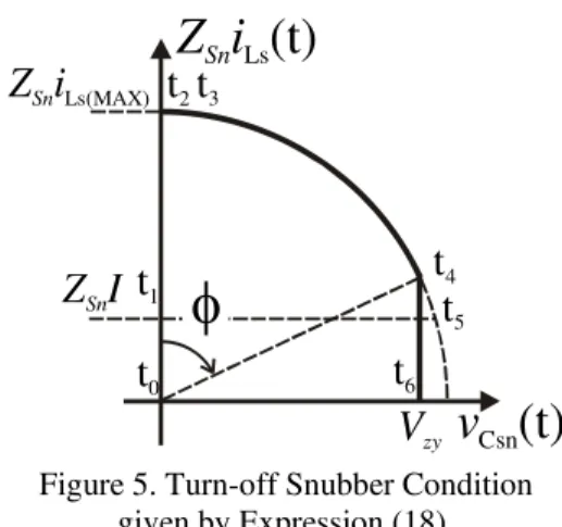
Expression above is graphically represented in the state-plane ZSniLs x vCsn, shown in Fig. 5.
Once that (18) is true, CSn can be chosen to optimize the
switching conditions of main switch during its turn-off by the expression below,
(
/)
Sn Sa MAX
C ≥I dv dt (19)
In order to ensure low current stresses and conduction losses through the auxiliary circuit snubber capacitors CS
and CSa can be made the smallest possible. This way, they
are considered as the intrinsic output capacitances (Coss) of
each switch, respectively.
( )
S oss
C =C S (20)
( )
Sa oss a
C =C S (21)
As CS and CSa guarantee low conduction losses, inductor LS
can be chosen to optimize the turn-off conditions of the main diode D. Therefore,
(
/)
S ZY D MAX
L ≥V di dt (22)
4 COMPARATIVE
ANALYSIS
To evaluate the gains obtained by the proposed snubber design optimization, the converter with SAAS presented in (Yaakov et al., 1995) is implemented using both design guidelines, the original design guidelines provided in (Yaakov et al., 1995) and the design guidelines described in previous section (Section 3). Table 1 gives the converter specifications.
4.1 Design guidelines from reference
(Yaakov et al., 1995)
By (Yaakov et al., 1995) the resonant auxiliary elements are calculated using expressions (16), (17) and (23).
(
) (
/)
Sn ZY S Sa MAX
C = I+V Z dv dt (23)
As LS and CS are function of kI and tZVS, expressions (16)
and (17) are depicted in Fig. 6 for a range of values of kI
(1.0 to 2.0) and tZVS (2% to 20%T), where the converter
operation period T is given by
T
=
1
f
s. From (Yaakov et al., 1995) typical values of kI lie in the range of 1.3 and1.5, whilst tZVS is in the range of 2% to 3% of T for Power
Factor Correction (PFC) applications (Bazinet and O'Connor, 1994). and in the range of 10% to 15% for DC-DC applications (Zhu and Ding, 1999). For comparative purposes, kI is chosen equal to 1.4 and tZVS equal to 10% T.
By means of Fig. 6, LS and CS are found as, 35μH and
1.8nF, respectively. By expression (23), CSn is calculated
equal to 2.8nF.
v
Csn(t)
Z i
Sn Ls(t)
V
zyZ i
Sn Ls(MAX)Z I
Snt
0t
1t
2t
3t
6t
4φ
t
54.2 Design guidelines from Section III
Once that condition given by expression (18) is ensured, the auxiliary elements are calculated by expressions (19) and (22), as LS= 4μH, CSn= 2.7nF (IRF840) and CS is the output
capacitance of the MOSFET (0.4nF) itself. Due to the non-linear characteristic of the MOSFET output capacitance (Coss) it is estimated as two or three times smaller than the
value presented by the data sheet (Coss= 310pF, VDS= 25V)
(International Rectifiers, Application note), resulting in a value for CS of about 155pF. Therefore,
160.6
S S S
Z = L C ≈ Ω.
5 EXPERIMENTAL
RESULTS
In order to compare the efficiency gain of the proposed optimized snubber design, the performance of the ZVT DC-DC PWM boost converter with SAAS (Streit and Tollik, 1991; Yaakov et al., 1995; Liu et al., 2000; Kim et al.,
2000; Menegáz et al., 1999) was evaluated on a 1 kW, 100
kHz laboratory prototype. The main converter parameters are summarized in Table 2. Two sets of auxiliary circuit elements were built. For the first set, the elements were specified following the design guidelines given by (Yaakov
et al., 1995) and presented in Section 4.1, Fig. 7(a). For the second set, the elements were specified following the optimized snubber design presented in Section 4.2, Fig. 7(b).
Moreover, a ZVT PWM boost converter with auxiliary DC voltage source, Fig. 7(c), was also compared. The parameters of this topology are given in Table 2. To reduce
LCSS
(H
)
an
d
(n
F
)
μ
t =2%Tzvs t =4%Tzvs t =6%Tzvs t =8%Tzvs t =10%Tzvs t =12%Tzvs t =14%Tzvs t =16%Tzvs t =18%Tzvs t =20%Tzvs t =10%Tzvs
C =1.8nFS
L =35 HS μ
( k )I
Figure 6. Representation of Expressions (16) and (17). Table 1. Specifications of power converter prototypes.
Parameter
Component ZVT PWM converter with snubber assisted auxiliary switch.
True-PWM ZVS pole boost converter.
V
i 150 V 150 V
V0 400 V 400 V
P0 1.0 kW 1.0 kW
fs 100 kHz 100 kHz
L 0.9 mH 0.9 mH
C 150 uF 150 uF
S IRFP450 IRFP450
S
a IRF840 HGTP3N60C3D
D MUR1560 MUR1560
Da1, Da2,Da3 RHR870 MUR1560
Vi
S
Sa
IRFP450 IRF840
MUR1560
Sk304 1N5306
150 V
4uH 2.2nF 0.47nF
150uF
910uH MUR1560 R
160 Ω
(a)
Vi S
Sa
IRFP450 IRF840
MUR1560
Sk304 1N5306
150 V
35uH 2.2nF
1.5nF
0.47nF
0.47nF
150uF
910uH MUR1560 R
160 Ω
(b)
IRFP450
MUR1560
MUR1560 MUR1560
150 V 5.1nF
150uF
910uH R
160 Ω
S
Da1
Da2
Tap Tas
Vi
L
Da3
Sa
Lsat
Ls
MUR1560
HGTPS3N60C3D 30turns 10turns 4.7uH
(c)
Figure 7. Diagrams of Implemented Prototypes. ZVT PWM boost converter with SAAS: (a) By Snubber Improved Design; (b) By Design of (Yaakov et al., 1995) (c)
True-PWM ZVS Pole Boost Converter (Martins et al., 1993).
Table 2. Auxiliary Circuit Parameters.
Parameter
ZVT PWM converter with SAAS. Component
Proposed Ref [16].
True PWM ZVS pole boost converter, ref. [5].
LS 4μH 35μH 3.7μF(+L k=1uF)
Cs 0.4nF 1.8nF 5.1 nF
CSn 2.7nF 2.8nF ---
F. Core ---- ---- EE-30/14
the auxiliary semiconductors and coupled inductors parasitic capacitance effects, a saturable inductor, implemented with 8 turns on a Toshiba “spike killer” core (SA 14x8x4.5) was used in series with LS.
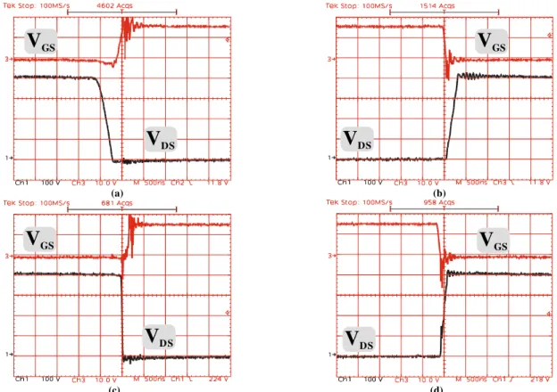
Fig. 8 shows the most relevant experimental waveforms obtained from the ZVT PWM boost converters with SAAS prototypes. It can be seen by the waveforms of voltage across the main switches that soft-switching conditions are achieved for main switch turn-on and turn-off processes, Fig. 8(a) and 8(c) for the original design guidelines and in Fig. 8(b) and 8(d) for the presented improved design guidelines, respectively.
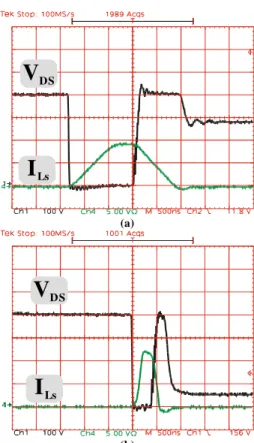
In Fig. 9 it can be seen that the maximum current through LS is slightly lower in the original design guidelines Fig.
9(a) than that in the presented improved design guidelines Fig. 9(b). However, the commutation time is higher in the original design guidelines, Fig. 9(a), which ensures low conductions losses to the presented improved design guidelines. In Fig. 9 it also can be seen that auxiliary switch turn-off is smooth due to the presence of CSn. Actually, a
perfect voltage turn-off of main switch cannot be achieved due to the voltage drop across CSn occurred at instant t6,
when the reverse recovery of diodes Da2 and Da3 take place.
Thus, turn-off losses of main switch are function of LS and
input current I.
Fig. 10 shows the waveforms in the snubber elements, LS
and CSn, where the above mentioned voltage drop can be
seen.
By Fig. 11 it can be seen that, at full load, the efficiency of the converter designed by the improved snubber design (circles) is about 0.5% higher and the average efficiency gain for the entire output range is higher than 0.5% compared to the original design (triangles). Besides, the improved snubber design also achieved higher efficiency for about 80% of entire load range compared to a True PWM ZVS pole boost converter (squares). As a result of the auxiliary circuit lower conduction, the ZVT PWM with SAAS with the proposed design presents higher efficiency in light and medium load condictions. This feature is offset by the turn-off losses of main switch, which are increased in high load conditions due to reverse recovery of auxiliary diodes.
To overcome this problem it is required to consider not only the main diode (D) di/dt requirements but also the auxiliary diodes di/dt to compute the auxiliary inductor LS.
However, a trade-off between the auxiliary circuit conduction losses and turn-off losses of main switch should be defined and adopted to calculate LS. With this trade-off
the efficiency may be even improved.
V
GSV
DSV
GSV
DS(a) (b)
V
GSV
DSV
GSV
DS(c) (d)
Figure 8. Main Switch Experimental Waveforms. (a) and (b) For Original Design Guidelines; (c) and (d) For Presented Improved Design Guidelines.
6 CONCLUSION
This paper presented an improved design to calculate the auxiliary elements of the ZVT DC-DC PWM converters with snubber assisted auxiliary switch. The presented design guidelines are based on the unique location of the turn-off snubber capacitor shared by the active switches. As the snubber energy does not circulate through auxiliary inductor, a reduction of the auxiliary circuit conduction losses can be achieved. As a result, converter efficiency can be improved.
Theoretical analysis is confirmed by the comparison of experimental results obtained from two prototypes designed by the presented improved design guidelines and by the original ones (Yaakov et al., 1995). The results show an efficiency gain higher than 0.5% for entire output power range.
In addition, experimental results also have shown that with the improved design the ZVT PWM converters with SAAS can be competitive with ZVT PWM converters with constant auxiliary voltage source (True PWM ZVS pole) in a large load range, which makes the ZVT with SAAS
converter a strong candidate for PFC applications. On the other hand, the ZVT with SAAS converter presented smaller efficiency at full-load (20%), its smaller component count and design simplicity still make it competitive, when compared to the True PWM ZVS pole converter.
ACKNOWLEDGMENT
The authors would like to express their gratitude to
I
LsV
DS(a)
I
LsV
DS(b)
Figure 9. Auxiliary Switch Experimental Waveforms. (a) For Original Design Guidelines; (b) For Presented
Improved Design Guidelines.
Scales: ILs: 5 A/div; VCsn: 100 V/div; Time – 500 ns/div.
I
LsV
Csn(a)
I
LsV
Csn(b)
Figure 10. Snubber Elements Experimental Waveforms. (a) For Original Design Guidelines; (b) For Presented
Improved Design Guidelines.
Scales: ILs: 5 A/div; VCsn: 100 V/div; Time – 500 ns/div.
400 500 600 700 800 900 1000 0.96
0.97 0.98 0.99
η
P
0True PWM ZVS Pole
ZVT PWM with S.A.A.S. (original) ZVT PWM with S.A.A.S. (improved)
“Coordenação de Aperfeiçoamento de Pessoal de Ensino Superior – CAPES” and “Conselho Nacional de Desenvolvimento Científico e Tecnológico – CNPq” (proc. 308865/2003-0 and proc. 141914/ 2003-3) for financial support, Icotron – an EPCOS Company and Thornton Inpec Eletrônica Ltda for material support.
REFERENCES
Bazinet, J., O’Connor, J. A. (1994). “Analysis and Design of a Zero Voltage Transition Power Factor Correction Circuit”, in IEEE Applied Power Electronics Conference , pp. 591-597.
Erickson, R. W., Maksimovic, D. (2001). Fundamentals of Power Electronics, University of Colorado, Bolder, Colorado, 2nd edition, pp. 92-100.
Filho, N. P., Farias, V. J., Freitas, L. C. (1994). “A Novel Family of DC-DC PWM Converters Using the Self-Resonance Principle”, in IEEE Power Electronics Specialists Conference, pp. 1385-1391.
Gegner, J. P., Lee, C. Q. (1994). “Zero-Voltage-Transition Converters Using a Simple Magnetic Feedback Technique”, in IEEE Power Electronics Specialists Conference, pp. 590-596.
Gegner, J.P., Lee, C.Q. (1994). “Zero-Voltage-Transition Converters Using an Inductor Feedback Technique”, in IEEE Applied Power Electronics Conference, Vol.2, pp. 862-868, Ninth Annual.
Hua, G., Leu, C.-S., Lee, F. C. (1992). “Novel Zero-Voltage-Transition PWM Converters”, in IEEE Power Electronics Specialists Conference, pp. 55-60.
Hua, G., Leu, C.-S., Lee, F. C. (1995). “Soft-Switching Techniques in PWM Converters”, in IEEE Trans. On Industrial Electronics, Vol. 42, Issue 6, pp. 595-603. International Rectifiers Application note, “A More Realistic
Characterization Of Power MOSFET Output Capacitance Coss”, AN-1001.
Jain, N., Jain, P., Joós, G. (2001). “Analysis of a Zero Voltage Transition Boost Converter using a Soft Switching Auxiliary Circuit with Reduced Conduction Losses”, in IEEE Power Electronics Specialists Conference, Vol. 4, pp. 1799-1804.
Kim, T.-W., Kim, H. –S., Ahn, H. –W. (2000). “An Improved ZVT PWM Boost Converter”, in IEEE Power Electronics Specialists Conference, Vol. 2, pp. 615-619.
Lee, F. C., Lin, R. L., Zhao, Y. (1998). “Improved Soft-Switching ZVT Converters with Active Snubber”, in
IEEE Applied Power Electronics Conference, Vol. 2, pp. 1063-1069.
Liu, H. –F., Liu, Y. –H. and Tzou, Y. –Y. (2000). “Implementation of ZVT Soft Switching Technique in a Single-Phase PFC Rectifier for Server Power Supply”. in IEEE Power Electronics and Motion Control Conference PIEMC 2000, pp. 584-589, Vol. 2. Martins, D. C., Brilhante, J. A., Seixas, F. J., Barbi, I.
(1993). “Buck PWM Converter Using a New ZVS Commutation Cell – Design and Experimentation”, in COBEP 93, pp. 93-98.
Menegáz, P. J. M., Có, M. A., Simonetti, D. S. L., Vieira, J. L. F. (1999). “Improving the Operation of ZVT DC-DC Converters”, in IEEE Power Electronics Specialists Conference, pp. 293-297.
Moschopoulos, G., Jain, P., Joos, G. (1995). “A Novel Zero-Voltage Switched PWM Boost Converter”, in
IEEE Power Electronics Specialists Conference, pp. 694-700.
Stein, C. M. O., Hey, H.L. (1998). “A New Family of Soft-Switching DC-DC PWM Converters Using a True ZCZVT Commutation Cell”, in IEEE IECON 98, pp. 1030 –1035.
Streit, R., Tollik, D. (1991). “A High Efficiency Telecom Rectifier Using A Novel Soft-Switched Boost-Based Input Current Shaper”, inINTELEC, pp. 720-726 Trivedi, M., Shenai, K. (1999). “Evaluation of Planar and
Trench IGBT for Hard- and Soft-Switching Performance” in Proc. of IEEE Industry Application Society Annual Meeting IAS’99, pp.717-721;
Tseng, C.-J., Chen, C.-L. (1998). “Novel ZVT-PWM Converters With Active Snubbers”, in IEEE Transactions on Power Electronics, Vol. 13, n. 5, pp. 861-869.
Xu, D. M., Zhang, J. M., Ren, Y. C., Qian, Z. (2000). “A Novel Single-Phase Active-Clamped ZVT-PWM PFC Converter”, in IEEE Applied Power Electronics Conference, p. 456-459.
Yaakov, S. B., Ivensky, G., Levitin, O. and Treiner A. (1995). “Optimization of the Auxiliary Switch Components in a Flying Capacitor ZVS PWM Converters”, in IEEE Applied Power Electronics Conference, pp. 503-509.
Yang, L., Lee, C. Q. (1993). “Analysis and Design of Boost Zero-Voltage-Transition PWM Converter”, in IEEE Applied Power Electronics Conference, pp. 707-713. Zhu, J. Y. and Ding, D. (1999). “Voltage- and