E
ff
ect of Nb doping on sintering and dielectric properties of PZT
ceramics
Ali Mirzaei
1,∗, Maryam Bonyani
1, Shahab Torkian
21Department of Materials Science and Engineering, Shiraz University, Shiraz, Iran
2Materials Engineering Department, Malek Ashtar University of Technology, Shahin Shahr, Iran
Received 8 June 2016; Received in revised form 18 August 2016; Accepted 27 September 2016
Abstract
The extensive use of piezoelectric ceramics such as lead zirconate titanate (PZT) in different applications be-came possible with the development of donor or acceptor dopants. Therefore, studies on the effect of dopants on the properties of PZT ceramics are highly demanded. In this study undoped and 2.4 mol% Nb-doped PZT (PZTN) powders were successfully obtained by a solid-state reaction and calcination at 850 °C for 2 h. Crys-tallinity and phase formation of the prepared powders were studied using X-ray diffraction (XRD). In order to study morphology of powders, scanning electron microscopy (SEM) was performed. The crystalline PZT and Nb-doped PZT powders were pelleted into discs and sintered at 1100, 1150 and 1200 °C, with a heating rate of 10 °C/min, and holding time of 1–6 h to find the optimum combination of temperature and time to produce high density ceramics. Microstructural characterization was conducted on the fractured ceramic surfaces us-ing SEM. Density measurements showed that maximal density of 95% of the theoretical density was achieved after sintering of PZT and PZTN ceramics at 1200 °C for 2 h and 4 h, respectively. However, the results of dielectric measurements showed that PZTN ceramics have higher relative permittivity (εr ∼17960) with lower Curie temperature (∼358 °C) relative to PZT (εr = 16000 at∼363 °C) as a result of fine PZTN structure as
well as presence of vacancies. In addition, dielectric loss (at 1 kHz) of PZT and PZTN ceramics with 95% theoretical density was 0.0087 and 0.02, respectively. The higher dielectric loss in PZTN was due to easier domain wall motions in PZTN ceramics.
Keywords: PZT, Nb2O5doping, powder synthesis, sintering, microstructure, permittivity
I. Introduction
Lead zirconate titanate (PZT) has perovskite struc-ture with general formula of ABO3. When Zr:Ti ratio is smaller than 95:5 all of compositions are ferroelectric at room temperature [1]. Above the Curie temperature, its unit cell is cubic, but below of the Curie temperature, it is distorted to either tetragonal (Zr:Ti<53:47) or rhom-bohedral (Zr:Ti>53:47). The boundary between these two phases (Zr:Ti∼53:47 at RT) is known as the mor-photropic phase boundary (MPB). In the 1950s, it was discovered that PZT ceramics with a Zr:Ti ratio approx-imately 52:48 have excellent properties, such as high Curie temperature, high electromechanical coupling co-efficient, easy poling and doping, and high dielectric, ferroelectric and piezoelectric properties [2,3]. It was
∗Corresponding author: tel:+98 71 3721 1984,
fax:+98 71 3721 1984, e-mail:[email protected]
shown that the coexistence of tetragonal and rhombo-hedral phases is responsible for the excellent proper-ties of PZT ceramics [4–6]. Due to exceptional prop-erties, PZT ceramics are used in numerous applications, such as phonograph pickups, air transducers, underwa-ter sound and ultrasonic generators, delay line trans-ducers, wave filters, etc. [7,8]. For these applications, high dielectric constant and good ferroelectric proper-ties, such as low coercive field (Ec), high remnant
po-larization (Pr) and high dielectric constant (εr) are de-sired. These properties can be tuned by doping PZT ce-ramics with donor dopants like Nb5+, Sb5+and Ta5+, or
acceptor dopants such as La3+. Furthermore, the
soft PZT ceramics are obtained by doping with donor dopants, such as W6+(for site A) and Nb5+, Sb5+ (for
site B), leading to the creation of vacancies on “A” site in the lattice. High domain wall mobility and resulting soft ferroelectric behaviour are characteristics of these doped ceramics. These features lead to large piezoelec-tric charge coefficient, moderate permittivity and high coupling factors which make them interesting for actu-ators, sensors, ultrasonic transmitters and receivers for flow or level measurement [11,12].
The main drawback of the pure PZT material for high advanced applications is the poor dielectric, ferro-electric and piezoferro-electric properties due to limited do-main movement [3]. In most cases, high-performance PZT ceramics with enhanced dielectric, piezoelectric and ferroelectric properties can be obtained using donor dopants such as Nb5+[13]. Although the effect of Nb5+
doping in PZT thin films is extensively studied [13–15], there are only a few papers about Nb5+ doping in bulk
(PZTN) ceramics [16,17], which are mostly focused on piezoelectric properties. The present work concerns the synthesis of PZT and PZTN powders via solid-state re-action and investigation of sintering behaviour and di-electric properties.
II. Experimental procedure
2.1. Solid-state synthesis
PbO (Merck 99%), TiO2 (rutile, Aldrich 99.8%), ZrO2, (Aldrich 99%) and Nb2O5 (Merck 99.5%) were used as starting materials without further purification. The precursor oxides were weighed according to de-sired stoichiometry of the final products, i.e. the pure PZT (Pb(Zr0.52Ti0.48)O3) and 2.4 mol% Nb2O5 doped PZT (Pb(Zr0.52Ti0.48)0.976Nb0.024O3) powders. Then the powders were put into a jar containing zirconia balls and isopropanol as milling medium. After the wet milling for 24 h, dry powders were obtained by evaporation of isopropanol at 85 °C for 2 h. The dried powders were ground in an agate mortar and finally calcined at 850 °C for 2 h to obtain desired perovskite phase (Fig. 1). Cal-cination was done in the zirconia crucibles with heat-ing rate of 5 °C/min. During cooling step, when the temperature of furnace reached 350 °C (estimated Curie temperature), the powders were air quenched. In order to obtain a homogeneous distribution of particles and breaking of big agglomerates formed during calcination, the second stage of ball milling was done for 12 h. Fi-nally, a high energy ball milling was performed on the powders for 4 h to further downsize the particles. The parameters of ball milling and high energy milling are presented in Table 1.
2.2. Shaping and sintering
The prepared PZT and PZTN powders calcined at 850 °C were used for preparation of ceramic discs. The powders were mixed with 5 wt.% of a water solution containing 10% polyvinyl alcohol (PVA) and pressed
into discs with 10 mm in diameter and 1–2 mm in thick-ness in stainless steel dies under uniaxial pressure of 150 MPa. The pressed discs were placed in a covered alumina crucible where atmosphere was controlled by the addition of the pure PZT (52/48)+10% ZrO2 pow-ders in the crucible without contact with the samples (Fig. 1). The discs were sintered at 1100, 1150 and 1200 °C for 1–6 h, with 4 h holding at 550 °C to burn-out the binder. The initial heating rate was set to be 5 °C/min up to the burn-out temperature and then a heating rate of 10 °C/min was used up to the final sintering temper-ature.
Figure 1. As-prepared and calcined PZT powders and sintered PZT sample (with set-up used for sintering)
Table 1. Parameters of ball milling and high energy milling
Parameter Ball milling High energy milling Diameter of balls 10 mm 1 mm
RPM 100 300
Powders to balls weight ratio
1:10 1:15
Powders to isopropanol weight ratio
1:1 1:1
2.3. Characterization
The phase formation of the powders and sintered bodies was examined by X-ray diffractometer (Brucker, Germany) using CuKα radiation (λ = 1.5418 Å). The XRD patterns were recorded at room temperature at a scan rate 0.05°/s. Particle size distribution was mea-sured using a laser particle size analyser (Horiba, LB-550, Japan), dispersing a small amounts of the powder in water and left in an ultrasonic bath before measure-ments. Microstructure characterization was conducted on the fractured sample surfaces by scanning electron microscopy (SEM, Cambridge, UK). The density of the sintered samples was determined by the Archimedes method using distilled water.
2.4. Dielectric measurements
Figure 2. Phases in PbO-ZrO2-TiO2system as a function of temperature [18]
III. Results and discussion
3.1. Characterization of PZT and PZTN powders PZT formation mechanism during calcination pro-cess is shown in Fig. 2. PZT is formed as a result of three sequential reactions [18]:
PbO+TiO2−−−→PbTiO3 (1) PbTiO3+PbO+ZrO2−−−→Pb(Zr1
−x,Tix)O3 (2) Pb(Zr1−x,Tix)O3+PbTiO3 −−−→Pb(Zr1
−y,Tiy)O3 (3) In the first reaction that occurs between 350–680 °C, PbO diffuses into TiO2. In this stage amounts of PbO and TiO2 gradually decrease and a new phase, i.e. PbTiO3 phase is formed, while the amount of ZrO2 is constant. In the second reaction, which occurs
be-tween 620–800 °C, amount of PbTiO3 phase decreases and Pb(Zr1-x,Tix)O3 (PZT) as a new phase is formed. With increase of temperature the amount of this phase increases. At the end of this stage, PbO, TiO2 and ZrO2totally disappear. In the third reaction which starts at 800 °C, amount of Pb(Zr1-x,Tix)O3 phase increases, while PbTiO3 phase decreases.
During calcination of PZT powders usually two crystalline structures are observed. The first one is a stable and desired structure with excellent electrical properties, i.e. perovskite with general formula ABO3 (Pb(Zr1-xTix)O3). The second one is a metastable and undesired structure, i.e. pyrochlore phase with poor electrical properties due to large defect density as a result of oxygen or lead deficiency, with general for-mula A2B2O7-x (Pb2(Zr1-xTix)2O7-x) [19]. As the main purpose of calcination process is to reach desired per-ovskite structure, it is essential to avoid formation of pyrochlore structure during calcination process.
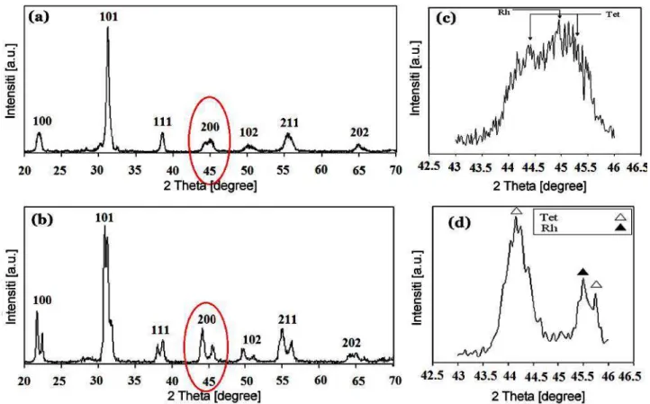
Figures 3a and 3b show XRD patterns of the cal-cined PZT and PZTN powders, respectively. All peaks can be indexed as perovskite PZT structure. If PbO is added in excess (above the stoichiometry), in addition to perovskite, another phase will be formed due to im-possibility of vacancy creation in B site [2]. Thus, the presence of only perovskite structure in the calcined powders (Fig. 3a,b) confirms good design of the used synthesis and calcination processes. Figures 3c and 3d show enlarged XRD patterns (2θ=42.5–46.5°) of PZT and PZTN powders, respectively. Coexistence of
Figure 4. Particle size distribution of: a) PZT and b) PZTN powders prepared by solid-state reaction and calcined at 850 °C for 2 h, after high energy ball milling
Figure 5. SEM micrograph of PZTN powders calcined at 850 °C for 2 h
Figure 6. FTIR spectra of PZT and PZTN powders calcined at 850 °C for 2 h
gonal and rhombohedral phases in perovskite structure of PZT is clearly observed (Fig. 3c). In fact, due to inho-mogeneity of chemical composition resulted from solid-state reaction, tetrahedral and rhombohedral phases are distinguishable. The clear separation between tetrahe-dral and rhombohetetrahe-dral phases in PZTN discs (Fig. 3d) can be attributed to the presence of Nb5+in the structure
that causes more inhomogeneity of chemical composi-tion within the grains [20].
Figures 4a and 4b show particle size distribution of the PZT and PZTN powders calcined at 850 °C for 2 h
followed by high energy ball milling, respectively. A salient feature of these powders is that they have rel-atively narrow distribution and the mean particle size approximately in the range 3–4µm.
Figure 5 shows SEM micrograph of PZTN powders after calcination at 850 °C for 2 h. As it can be seen, the powders have relatively narrow distribution with aver-age particle size about 3–3.5µm, which is in agreement with PSA results.
Figure 6 shows FTIR spectra of PZT and PZTN pow-ders after calcination at 850 °C for 2 h. A sharp band at 582.5 cm-1 was formed and can be attributed to the M–O bonding (M=Ti, Zr, Nb and Pb) [21]. The O–H peaks are not observed in FTIR spectra of these powders due to high calcination temperature. There is no signifi-cant difference between FTIR spectra of PZT and PZTN powders, because Nb5+ions replace Ti4+/Zr4+ions and
make Nb–O bonds with FTIR peak at 585.5 cm-1 (simi-lar to the positions of Ti–O or Zr–O bonds).
3.2. Sintering behaviour of PZT and PZTN ceramics There are several reasons why a high density fer-roelectric ceramics are required in most applications. Firstly, dielectric constant of ferroelectric ceramics in-creases with increasing density, because the relative di-electric constant of pores/vacuum is unit. Secondly, the presence of pores generally causes high dielectric loss,
since porosity could provide conduction path for elec-tricity. Moreover, mechanical strength is directly deter-mined by density of a material. Finally, electrical con-duction caused by porosity is also responsible for de-graded electrical breakdown strength [22].
Figure 7 shows density of PZT discs as a function of temperature and time. PZT discs sintered at 1100 °C for 2 h had relative density of 88 %TD (theoretical density) which continuously increased with sintering time. Thus, relative density of 95 %TD was reached after sintering at 1100 °C for 6 h. At 1150 °C, with increase of time to 4 h there is obvious increase of density (Fig. 7), due to the increase of diffusion rate and improvement of sin-tering process. However, with further increase of time to 6 h, density drops due to evaporation of lead oxide, grain growth and presence of pores insides the grains (Fig. 8) [23]. At 1200 °C, optimum sintering time was 2 h, which was enough to reach 95 %TD. With further increases of time to 4 h or 6 h, due to vaporization of PbO and grain growth (Fig. 9), it was impossible to reach higher den-sities.
In order to improve electrical properties of PZT ceramics and grain growth inhibition during sinter-ing, PZT ceramics with 2.4 mol% Nb2O5 were pre-pared. Due to presence of small interstitial sites in the perovskite structure (Fig. 10) and ionic radius of Nb5+ (0.78 Å), Zr4+ (0.86 Å), Ti4+ (0.745 Å) and Pb2+
(0.133 Å) [25], it is expected that Nb5+substitutes Zr4+
and Ti4+ on B-site in perovskite structure. However,
when a doped ions are added in perovskite structure, electrical neutrality must always remain unchanged. Thus, by the substitution of Nb5+ ion on B-site,
addi-tional positive charge is introduced and Pb2+vacancies
are created to maintain charge neutrality, leading to for-mation of soft PZT. For every two Nb5+ions introduced
into the lattice, one Pb2+ vacancy is formed. This
va-cancy pair can align itself with polarization of PZTN and due to the increased mobility of domain walls, could improve permittivity of PZTN.
Figure 11 presents density of PZTN ceramics as a function of temperature and time. As it can be seen, sin-tering temperature of 1150 °C is not sufficient to reach a high value of density as the obtained highest density was∼90 %TD. Therefore, the PZTN ceramics were sin-tered at 1200 °C and 93 %TD and 95 %TD were ob-tained after 2 h and 4 h, respectively (Fig. 11). That is the maximum density for PZTN ceramics. Incorpora-tion of Nb5+into structure of PZT causes formation of
Pb vacancies and improved diffusion and final density. However, created Pb vacancies as a result of Nb5+
addi-tion have electrical charge and low mobility [26]. There-fore, these samples need higher sintering temperature or longer sintering time than the pure PZT. In fact high density of PZTN ceramics is principally due to grain growth inhibition (Fig. 12) [25]. Nb5+ ions precipitate
near grain boundaries and lead to significant reduction of their movement. When boundary moves, it must take precipitated ions with itself. This causes decrease of
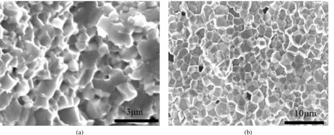
Figure 8. SEM micrograph of PZT ceramics sintered at 1150 °C for 6 h
(a)
(b)
Figure 9. SEM micrographs of fracture surface of PZT discs calcined at 1200 °C for: a) 2 h and b) 6 h
Figure 11. Density of PZTN ceramics as a function of sintering temperature and time
grain boundary mobility and eventually creation of fine grain structure and improvement of electrical properties of PZTN ceramics [24].
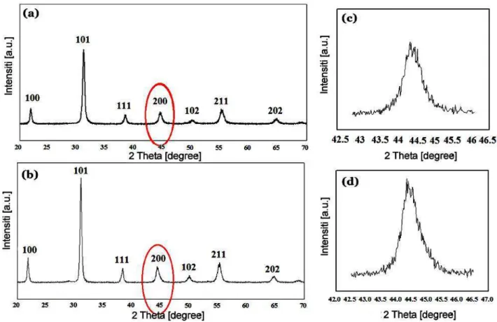
Figures 13a and 13b show the XRD patterns of PZT and PZTN ceramic discs after sintering at 1200 °C for 2 and 4 h, respectively. Compared with XRD patterns of PZT and PZTN powders (Fig. 2), no additional phase is formed. Furthermore, the peaks are sharper, indicat-ing grain growth durindicat-ing sinterindicat-ing at high temperature. Figures 13c and 13d show enlarged XRD patterns of the circled area in corresponding XRD patterns. It can be seen that splitting of tetragonal and rhombohedral phases is decreased which can confirm better chemi-cal homogeneity in the sample sintered at high temper-atures.
A serious problem in preparation PZT ceramics is preserving the desired composition due to the fact that the evaporation of lead oxide leads to change of the sto-ichiometry. The weight of the samples before and af-ter sinaf-tering was measured by a sensitive balance and the difference between these two values was reported as mass loss after sintering. Mass losses after sintering at
1150 °C for 4 h are 3.4% and 3% for PZT and PZTN ce-ramics, respectively. Somewhat higher mass losses were observed at 1200 °C for 4 h, i.e. 4% and 3.5% for PZT and PZTN ceramics, respectively. In the present case, the mass loss, related to the volatilization of lead ox-ide and PVA used as binder, is higher for the pure PZT than for PZTN ceramics. In the case of PZTN, the main factor that controls PbO evaporation is the penetration of Nb5+ ions in perovskite structure. It was previously
reported [27] that dopants hinder the evaporation of the lead oxides. This can explain the relatively smaller mass loss of PZTN in comparison with the pure PZT ceram-ics.
3.3. Dielectric properties
Figure 14 shows variations of relative permittivity of PZT and PZTN ceramics (sintered at 1200 °C for 2 and 4 h, respectively) as a function of temperature. As it can be seen, upon doping with 2.4 mol% Nb5+ Curie
tem-perature of PZTN ceramics is lower for about 5 °C and relative permittivity is higher in comparison to the pure PZT samples. Thus, room temperature relative permit-tivity of PZTN is 1178, while that for PZT is 925. Also, maximum relative permittivity of PZT is ∼16000 and that for PZTN is ∼17960. Higher relative permittivity and lower Curie temperature in PZTN ceramics are due to the fact that domain wall motion becomes easier with donor dopant such as Nb5+. In fact due to presence of
vacancies in PZTN ceramics, domain walls move easier and align themselves by external electric field, resulting in better polarization and consequently higher dielectric constant [28].
Relationship between dielectric permittivity and the temperature above Curie temperature is described by Curie-Weiss law [29]:
εr=ε0+ C
T−T0 (4)
where ε0 is permittivity of vacuum (8.854×10⁻¹²F/m),
Cis Curie-Weiss constant,T0is Curie point (Curie
tem-(a) (b)
Figure 13. XRD pattern of: a) PZT discs sintered at 1200 °C for 2 h, b) PZTN discs sintered at 1200 °C for 4 h and corresponding enlarged XRD patterns (2θ=42.5–46.5°) – (c) and (d) respectively
Figure 14. Relative permittivity of PZT and PZTN ceramic discs as a function of temperature at 1 kHz
perature is about 10 °C lower than Curie point) andT
is temperature. According to above equation, with in-crease of temperature above Curie point, the permittiv-ity drops gradually. The same trend was observed for PZT and PZTN ceramics, where the permittivity of both materials decreases upon increase of the temperature above their corresponding Curie temperature.
Dielectric loss (at 1 kHz) for both PZT and PZTN ce-ramics were obtained. Dielectric loss at 1 kHz and room temperature for PZT and PZTN ceramics with 95 %TD was 0.0087 and 0.02, respectively. It is accepted that for ferroelectric ceramics whole dielectric loss is due to
do-main wall motion. In PZTN ceramics owing to the pres-ence of vacancies, domain walls can move more easily, therefore even under the small electrical field, domain walls move resulting in higher dielectric loss.
IV. Conclusions
In this study undoped PZT and 2.4 mol% Nb-doped PZT powders (PZTN) were successfully synthesized by solid-state reaction and calcined at 850 °C for 2 h. The calcined powders have perovskite structure with mix-ture of tetrahedral and rhombohedral phases and the av-erage particle size of 3–4µm. The optimal sintering con-ditions that produce ceramics with 95 %TD were found to be 1200 °C/2 h for PZT and 1200 °C/4 h for PZTN ceramics. The results of relative permittivity measure-ments indicate that PZTN ceramics had higher dielectric permittivity with lower Curie temperature as a result of fine structure as well as presence of vacancies. Also, di-electric losses (at 1 kHz) of PZTN ceramics were higher than PZT ceramics, due to easier movement of domain walls in PZTN ceramics.
Acknowledgement: Fruitful discussions with Dr. Feizpour are greatly acknowledged.
References
with a polymer precursor”, Mater. Lett., 57 (2003) 2432–2442.
2. B. Jaffe, W.R. Cook, H. Jaffe,Piezoelectric Ceram-ics, Academic Press, London, UK, 1971.
3. A. Rachakom, S. Jiansirisomboon, A. Watcharapa-sorn, “Physical and electrical properties of Nb doped Bi0.5Na0.5[Zr0.59Ti0.41]O3”, Ceram. Int., 38 (2012) S385–389.
4. B. Jaffe, W.R. Cook, H. Jaffe, “Piezoelectric ceram-ics”,J. Sound Vib.,20(1971) 562–563.
5. B. Noheda, D.E. Cox, “Bridging phases at the mor-photropic boundaries of lead-oxide solid solutions”,
Phase Transitions,79(2006) 5–20.
6. M. Hinterstein, M. Hoelzel, J. Rouquette, J. Haines, J. Glaum, H. Kungl, M. Hoffman, “Interplay of strain mechanisms in morphotropic piezoceramics”, Acta Mater.,94(2015) 319–327.
7. K. Uchino, Ferroelectric Devices, Marcel Dekker,
USA, 2000.
8. L.M. Levinson, Electronic Ceramics: Properties,
Devices and Applications, Marcel Dekker, USA,
1988.
9. M.I. Morozov, D. Damjanovic, “Charge migration in Pb(Zr,Ti)O3 ceramics and its relation to ageing, hardening, and softening”,J. Appl. Phys.,107(2010) 034106.
10. N. Horchidan, C.E. Ciomaga, R.C. Frunza, C. Capi-ani, C. Galassi, L.Mitoseriu, “A comparative study of hard/soft PZT-based ceramic composites”, Ceram. Int.,42(2016) 9125–9132.
11. P.S. Silva Jr., M. Venet, O. Florencio, “Influence of diffuse phase transition on the anelastic behavior of Nb-doped Pb(Zr0.53Ti0.47)O3 ceramics”,J. Alloys
Compd.,647(2015) 784–789.
12. M.M.S. Pojucan, M.C.C. Santos, F.R. Pereira, M.A.S. Pinheiro, M.C. Andrade, “Piezoelectric properties of pure and (Nb5+,Fe3+) doped PZT
ce-ramics”,Ceram. Int.,36(2010) 1851–1855.
13. E.C.F. Souza, A.Z. Simoesa, M. Cilensea, E. Lon-goa, J.A. Varela, “The effect of Nb doping on fer-roelectric properties of PZT thin films prepared from polymeric precursors”,Mater. Chem. Phys.,88 (2004) 155–159.
14. V. Kayasu, M. Ozenbas, “The effect of Nb doping on dielectric and ferroelectric properties of PZT thin films prepared by solution deposition”,J. Eur. Ce-ram. Soc.,29(2009) 1157–1163.
15. T. Haccart, D. Remiens, E. Cattan, “Substitution of Nb doping on the structural, microstructural and electrical properties in PZT films”,Thin Solid Films,
423(2003) 235–242.
16. M. Pereira, A.G. Peixoto, M.J.M. Gomes, “Effect of Nb doping on the microstructural and electrical prop-erties of the PZT ceramics”,J. Eur. Ceram. Soc.,21 (2001) 1353–1356.
17. S.Y. Chu, T.Y. Chen, I.T. Tsai, W. Water, “Doping effects of Nb additives on the piezoelectric and di-electric properties of PZT ceramics and its applica-tion on SAW device”, Sensors Actuators A: Phys.,
113(2004) 198–203.
18. Y. Matsuo, H. Sasaki, “Formation of lead zirconate-lead titanate solid solutions”,J. Am. Ceram. Soc.,48 (1965) 289–291.
19. A. Mirzaei, M. Bonyani, S. Torkian, “Synthesis and characterization of nanocrystalline PZT powders: From sol to dense ceramics”,Process. Appl. Ceram.,
10(2016) 9–16.
20. P. Amonpattaratkit, P. Jantaratana, S. Ananta, “In-fluences of PZT addition on phase formation and magnetic properties of perovskite Pb(Fe0.5Nb0.5)O3 -based ceramics”,J. Magn. Magn. Mater.,389(2015) 95–100.
21. T.I. Chang, J. Lhaung, H.P. Lin, S.C. Wang, H.H. Lu, L. Wu, J.F. Lin, “Effect of drying temperature on structure, phase formation, sol-gel derived lead zirconate titanate powders”, J. Alloys Compd.,414 (2006) 224–229.
22. P. Pramanik, R.N. Das, “Structure property relations of chemically synthesized nanocrystalline PZT pow-ders”,Mater. Sci. Eng. A,304-306(2001) 775–779. 23. M.N. Rahaman,Ceramic Processing and Sintering,
CRC Press, New York, USA, 2003.
24. R.B. Atkin, R.M. Fulrath, “Point defects and sinter-ing of lead zirconate titanate”, J. Am. Ceram. Soc.,
54(1971) 265–270.
25. M.W. Barsoum,Fundamental of Ceramics, IOP
Pub-lishing Ltd, USA, 2003.
26. M. Hammer, M.J. Hoffmann, “Sintering model for mixedoxide derived lead zirconate titanate ceram-ics”,J. Am. Ceram. Soc.,81(1998) 3277–3284. 27. J.F. Fernández, C. Moure, M. Villegas, P. Durán, M.
Kosec, G. Drazic, “Compositional fluctuations and properties of fine-grained acceptor-doped PZT ce-ramics”,J. Eur. Ceram. Soc.,18(1998) 1695–1705. 28. C.H. Wang, S.J. Chang, P.C. Chang, “Effect of
sinter-ing conditions on characteristics of PbTiO3-PbZrO3 -Pb(Mg1/3Nb2/3)O3-Pb(Zn1/3Nb2/3)O3”, Mater. Sci. Eng. B,111(2004) 124–130.
29. Y. Guo, K.I. Kakimoto, H. Ohsato, “Dielec-tric and piezoelec“Dielec-tric properties of lead-free (Na0.5K0.5)NbO3-SrTiO3 ceramics”, Solid State