INFLUENCE ON OPTICAL
PROPERTIES OF CADMIUM SULPHIDE
BY MANUAL DEPOSITION OF SILAR
METHOD
1.K. MANIKANDAN aResearch Scholar, Department of Physics,
Anna University of Technology Tiruchirappalli, Email:[email protected]
2.P.MANI Assistant Professor, Department of Physics,
Anna University of Technology Tiruchirappalli, Email:[email protected]
3.S. FERMI HILPERT INBARAJ Research Scholar,
Department of Physics,
Anna University of Technology Tiruchirappalli
4.S.VALLI, Research Scholar, Department of Physics,
AVVM. Sri Pushpam college, Thanjavur
5.Dr. J.Joseph Prince Assistant Professor, Department of Physics,
Anna University of Technology Tiruchirappalli,
ABSTRACT:
CdS thin films were deposited onto microscope glass slide from a chemical bath. The effect of molarity of the thin films was studied at 0.10M and 0.20M. The CdS film at the fundamental absorption region (200-800nm) was determined using the spectral data of transmittance and absorption. The direct band gap energies were determined and found to be 2.15 eV and 2.24 eV respectively. Meanwhile, from the band gap were observed to be mainly dependent on the molarity value.
Keywords. CdS, Absorbance, Transmittance, Band gap, thin film, molarity .
1. INTRODUCTION
SILAR deposition is known to be a simple, low temperature, and inexpensive large-scale deposition technique. It has been used in the deposition of semiconductor thin films for over forty years. Cadmium sulphide (CdS) a wide energy gap semiconductor has been emerged as an important material due to its applications in photovoltaic cell as window layers CdS in naturally an n-type material with an optical band gap of 2.4 eV. There are many techniques to prepare CdS films which including electrodeposition, pulsed-laser deposition, RF reactive sputtering, atomic layer epitaxy and chemical bath deposition method. Among these techniques, the manual (SILAR deposition) method is considered as very common technique. It is found to be a cheap and simple way to deposit large area polycrystalline metal chalcogenide thin films. The preparation CdS thin films using SILAR such as CdS, CdSe, Cd1-xZnxSe, were reported by several authors.
K. Manikandan et al. / International Journal of Engineering Science and Technology (IJEST)
In this paper, we studied the influence of molarity concentration on the spectral properties of manually deposited CdS thin films using UV-Visible Spectrometry. The studies of CdS thin films have been reported by many researchers. CdS films were deposited onto substrates using precursor such as Cadmium Nitrate and Sodium sulfide solutions. Here, we prepare CdS films from a chemical bath containing Cadmium Nitrate, Sodium sulfide solutions. The band gap of the thin films was investigated.
2. EXPERIMENTAL:
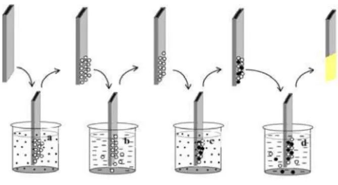
Micro glass slides (6 cm x 1.25 cm) were cleaned thoroughly using soap solution to remove visible impurities and kept in chromic acid for 2 hours. Later the slides were rinsed with distilled water. Samples were prepared, using In (NO3)3 as the cationic solution. The anionic precursor was Na2S solution. Molar ratio between Cadmium and Sulfur was kept 1:1 for all the samples. Dipping time in precursor solution was varied from 2s to 15s in both cases. Cleaned glass substrates were immersed for ‘4’ seconds in cationic precursor. This resulted in adsorption of cadmium ions on to substrate surface. It was then immersed in distilled water for ‘6’ seconds, in order to remove the de-adsorbed ions. These substrates were again immersed in for ‘4’ seconds in anionic precursor leading to adsorption and reaction of sulfide ions. Unreacted sulfide ions were removed by rinsing them in distilled water for ‘6’ seconds. Thus a SILAR cycle is completed after these four operations. Repetition of SILAR cycle resulted in deposition of a thin layer of CdS on the substrate. These samples were annealed in vacuum at 100 OC for one hour hot air oven.
Fig 1. Shows experimental set up of manually operated SILAR deposition system
( Schematic representation of SILAR method (a) cationic precursor and (c) anionic precursor and (b, d) deionised water.)
3. SPECTRAL STUDIES:
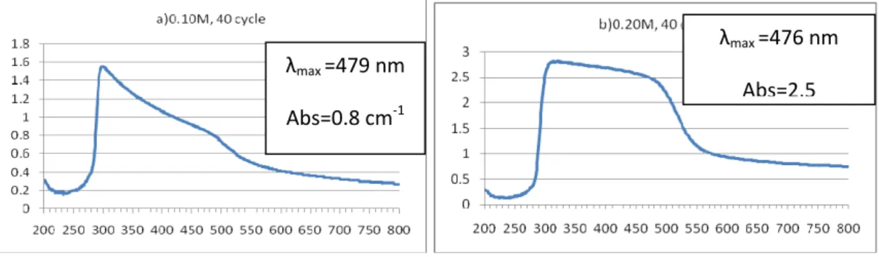
Absorption spectrum was recorded in a UV-VIS-spectrophotometer. Figure 2(a&b) shows the transmittance and absorption spectrum of CdS thin films deposited at different molarity concentration 0.10M and 0.20M .The spectra recorded for CdS films as a function of wavelength range 200-800 nm.
Fig 2. The transmission spectrum of CdS at two different concentrations.
It is observed that the transmittance decreases with increase in molarity of precursor solution. The film deposited with 0.10M shows higher transmittance compare to 0.20M. This property of high transmittance makes
K. Manikandan et al. / International Journal of Engineering Science and Technology (IJEST)
it a good material for optical coatings. The spectra revealed that the CdS films have low absorbance in the visible region, which is a characteristic of the transmittance edge was seen to be shifted slightly towards higher wavelength as the molarity concentration was increased. This shift indicates decrease in bandgap, which can be attributed to increase in the molarity concentration. Also figure 3 (a&b) shows the occurrence of peaks in the absorbance (transmittance) plot at 479nm and 476 nm. These peaks are attributed to the formation of excitons in CdS thin films, which was increased by increasing the molarity concentration .This first parameter (0.10M) influences a shift between the spectra , which means the increase of band gap energy. The band gap energies ‘Eg’ for CdS thin films have been found as 2.15eV and 2.24eV at room temperature respectively 0.10M and 0.20M concentration.
Fig 3. The absorbance spectrum of CdS at two different concentrations.
The optical energy band gap was estimated from the plots of (Absorbance)2 versus energy plots
(Eg=1240/λ) shown in Figure 4,where λ is the absorption wavelength, is Planck's constant and h is the frequency of the radiation. Since the plots are linear, the direct nature of the optical transition is confirmed. As we see in the (table.1) it is noticed that the band gap energy was slightly larger for the higher Molarity concentration. Optical band gap of CdS was found as 2.24 eV by Sankapal (1), Eg as 2.60 eV by Soumitra Patra(2) ,. A band gap of energy of 2.67 eV has been reported for CdS nanoparticles (~10 nm particle size) by chemical reduction method by Bhattacharya R and Saha S(3), The value of the optical energy gap for the deposited and annealed films was in the range(2.35-2.43) eV by M. A. Mahdi,(4) The estimated band gaps are in the range of 2–2.3 eV by M. Dhanam(5). 2.37 eV by Hua Sun and Jin Mu(6).,, 2.4 eV reported by Ramaiah et al(7) (2001).
a) 0 .10m 40 cycles,Eg= 2.15 eV
b) 0 .20m 40 cycles Eg=2.24 eV
Fig.4. Optical (absorbance)2 versus. energy plots of CdS films deposited with Different Molarity. (Bandgap Determination)
eV
0.10M, 40 cycle
0.20M, 40 cycle
(Absorbance)
2
(Absorbance)
2
λmax =479 nm
Abs=0.8 cm‐1
λmax =476 nm
Abs=2.5
K. Manikandan et al. / International Journal of Engineering Science and Technology (IJEST)
Table1.Optical Results.
S.No Molarity Cycle Wavelength Transmittance Absorbance Band gap
1 0.10M 40 479nm 54% 0.83 2.15eV
2 0.20M 40 476 19% 2.40 2.24eV
4. CONCLUSION:
It is observed that, optical band gap energy decreased from 2.24 eV to 2.15 eV with decreasing Molarity concentration.
ACKNOWLEDGEMENT
We would also like to acknowledge the financial support given by the Dr. J. Joseph Prince Assistant Professor Department of Physics, Anna University of Technology, Tiruchirappalli.
REFERENCES;
[1] B.R. Sankapal, R.S. Mane, C.D. Lokhande, Deposition Of Cds Thin Films By The Successive Ionic Layer Adsorption And Reaction (Silar) Method, Materials Research Bulletin 35 (2000) 177–184
[2] Soumitra Patra, Partha Mitra, Swapan Kumar Pradhan, Preparation Of Nanodimensional Cds By Chemical Dipping Technique And Their Characterization, Materials Research. 2011; 14(1): 17-20
[3] R Bhattacharya And S Saha, Growth Of Cds Nanoparticles By Chemical Method And Its Characterization Pramana Journal Of Physics Indian Academy Of Sciences Vol. 71, No. 1 July 2008 Pp. 187-192
[4] M. A. Mahdi1, S. J. Kasem1, J. J. Hassen1, A. A. Swadi2, S. K. J.A L-Ani,3 Structural And Optical Properties Of Chemical Deposition Cds Thin Films, Int. J. Nanoelectronics And Materials 2 (2009) 163-172
[5] Influence Of Preparation Technique On The Properties Of In:Cds Thin Films, M. Dhanam, B. Kavitha, B. Maheswari And G.R. Jesna, Vol. 119 (2011) Acta Physica Polonica A No. 6
[6] Hua Sun & Jin Mu Silar Deposition Of Cds Thin Films On Glass Substrates Modified With 3
-Mercaptopropyltrimethoxysilane,
Journal Of Dispersion Science And Technology Volume 26, Issue 6, 2005, Pages 719-722
[7] Kodigala Subba Ramaiah ;_R.D. Pilkington , A.E. Hill , R.D. Tomlinson , A.K. Bhatnagar, Structural And Optical Investigations On Cds Thin Films Grown By Chemical Bath Technique, Materials Chemistry And Physics 68 (2001) 22–30
K. Manikandan et al. / International Journal of Engineering Science and Technology (IJEST)