Structural, microstructural, and transport properties of highly oriented LaNiO 3 thin
films deposited on SrTiO 3 (100) single crystal
G. P. Mambrini, E. R. Leite, M. T. Escote, A. J. Chiquito, E. Longo, J. A. Varela, and R. F. Jardim
Citation: Journal of Applied Physics 102, 043708 (2007); doi: 10.1063/1.2769349
View online: http://dx.doi.org/10.1063/1.2769349
View Table of Contents: http://scitation.aip.org/content/aip/journal/jap/102/4?ver=pdfcov
Published by the AIP Publishing
Structural, microstructural, and transport properties of highly oriented
LaNiO
3thin films deposited on SrTiO
3„
100
…
single crystal
G. P. Mambrini and E. R. Leite
LIEC, Departamento de Química, Universidade Federal de São Carlos, Rod. Washington Luiz, km 235, CP 676, CEP 13565-905, São Carlos, SP, Brazil
M. T. Escote
Centro de Engenharia, Modelagem e Ciências Sociais Aplicadas, Universidade Federal do ABC, Rua Catequese 242, CEP 09090-900, Santo André, SP, Brazil
A. J. Chiquito
Departamento de Física, Universidade Federal de São Carlos, Rod. Washington Luiz, km 235, CP 676, CEP 13565-905, São Carlos, SP, Brazil
E. Longo and J. A. Varela
Instituto de Química, Universidade Estadual Paulista – Araraquara, R. Prof. Francisco Degni, s/n, CEP 14801-907, Araraquara, SP, Brazil
R. F. Jardim
Instituto de Física, Universidade de São Paulo, CP 66318, CEP 05315-970, São Paulo, SP, Brazil
共Received 3 April 2007; accepted 1 July 2007; published online 23 August 2007兲
Electrical conductive textured LaNiO3/ SrTiO3 共100兲thin films were successfully produced by the
polymeric precursor method. A comparison between features of these films of LaNiO3共LNO兲when
heat treated in a conventional furnace共CF兲and in a domestic microwave共MW兲oven is presented. The x-ray diffraction data indicated good crystallinity and a structural orientation along the共h00兲 direction for both films. The surface images obtained by atomic force microscopy revealed similar roughness values, whereas films LNO-MW present slightly smaller average grain size共⬃80 nm兲 than those observed for LNO-CF 共60–150 nm兲. These grain size values were in good agreement with those evaluated from the x-ray data. The transport properties have been studied by temperature dependence of the electrical resistivity共T兲which revealed for both films a metallic behavior in the entire temperature range studied. The behavior of共T兲was investigated, allowing to a discussion of the transport mechanisms in these films. ©2007 American Institute of Physics.
关DOI:10.1063/1.2769349兴
I. INTRODUCTION
Thin films of perovskite oxides with low electrical resis-tivity have been extensively studied due to the fact that such a physical property makes them suitable electrodes for per-ovskite ferroelectric layers in thin film capacitors.1–4The use of oxide electrodes with low electrical resistivity results in a pronounced decrease of fatigue, a limitation commonly ob-served when metal bottom electrodes are used. In fact, for Pb共ZrxTi1−x兲O3 共PZT兲 films deposited on oxide electrodes,
the number of cycles without fatigue was found to increase from 106 to 1010 cycles2,3 when metallic-like bottom elec-trodes based on perosvskite oxides are used. Within this con-text, several oxides with low electrical resistivity and perov-skite crystal structure have been investigated such as La0.5Sr0.5CoO3, SrRuO3, and LaNiO3 共LNO兲. All of them
display very low values of electrical resistivity at room tem-perature, typically of⬃10−4 ⍀cm, and have been used to
fabricate fatigue-free ferroelectric thin films.2–4 The LNO oxides crystallize in a perovskite structure with rhombohe-dral or pseudocubic distortion and lattice parameters c
⬇0.546 nm and a⬇0.384 nm, respectively.1 Their trans-port properties are also of interest and they display a metallic-like behavior in a wide range of temperature,
roughly from 1 to 1000 K. In addition to this, the perovskite LNO exhibits Pauli paramagnetism and does not undergo any phase transformation within this temperature interval.5,6 Many efforts have been used for preparing LNO thin films by different deposition techniques such as sputtering,7 pulsed laser deposition,8,9 molecular beam epitaxy,10 metal-organic decomposition,11 and sol-gel methods.12 More re-cently, an alternative route, based on a method of chemical solution deposition, called complex polymerization route, has been successful used for growing thin films of several oxides as, e.g., PZT,13,14BaTiO3,15SrTiO3,16LiNbO3,17and
LNO films.1 In all cases, the complex polymerization route allowed the production of stoichiometric films with excellent structural and electrical properties.
As far as these previous studies are concerned, polycrys-talline thin films were formed but without any appreciable preferred orientation. Then, one of the aims of this work is to study the experimental conditions to produce LNO thin films with a high degree of orientation. In fact, some changes in the experimental procedure can be made in order to obtain an oriented system. First of all, the LNO films can be deposited onto a preferred oriented single crystal, as LaAlO3 or even SrTiO3. This has been made, for example, by Bouquet et al.17 that obtained epitaxially growth of LiNbO3 films on
0021-8979/2007/102共4兲/043708/6/$23.00 102, 043708-1 © 2007 American Institute of Physics
sapphire substrate by the complex polymerization route. An-other route to obtain highly oriented thin films is by using a domestic microwave oven during the crystallization process. Such a procedure has been successfully applied for deposit-ing thin films of LiNbO3and SrBi2Nb2O9共Refs.18and19兲.
Also, LNO electrodes grown on LaAlO3 共100兲 substrates,
with 共100兲 crystallographic orientation, were also obtained by performing the heat treatment of the thin films in a mi-crowave oven.20By using a similar procedure, the same au-thors described the deposition of highly oriented Pb1−xBaxTiO3films with excellent electrical properties.20
We discuss here the general physical properties of highly oriented LaNiO3thin films grown by the complex
polymer-ization method on SrTiO3共100兲substrates. These films were characterized by structural, morphological, and electrical transport measurements. The thin films were heat treated in a conventional furnace and in a domestic microwave oven and their general physical properties were compared. We have also investigated the transport properties of these films, which allowed us a discussion concerning the transport mechanisms of these perovskite LaNiO3 thin films.
II. EXPERIMENTAL PROCEDURE
LaNiO3thin films were deposited on SrTiO3共100兲single
crystal substrates by spin coating solution deposition of a polymeric precursor. Details of the method employed are de-scribed elsewhere.1,20,21 After the deposition, the films are preliminary heat treated at 300 ° C in a conventional electric furnace in order to eliminate organic compounds and to ob-tain an amorphous and continuous inorganic film. The crys-tallization of these thin films was carried out in two different furnaces: 共a兲 in a conventional electric furnace operating at 700 ° C for 2 h and using a heating rate of 5 ° C / min; and共b兲 in a domestic microwave oven at 700 ° C for 10 min with a heating rate of 230 ° C / min. The microwave furnace used in these experiments is similar to the one described in Ref.18. The steps described previously were repeated until the films reached the desired thickness of⬃200 nm. The samples heat treated in the conventional furnace and in the microwave oven are thereafter referred to as LNO-CF and LNO-MW, respectively.
The structural features of the LaNiO3 thin films were
analyzed by x-ray diffraction 共XRD兲. These measurements were carried out in a Rigaku DMax 2500PC diffractometer by using CuK␣ radiation and 2 varying from 20° to 60°. The film thickness was inferred by direct observation of scanning electron microscopy 共SEM兲 images of the cross section of the films in a Zeiss DSM940A microscope. Atomic force microscopy 共AFM兲 was used to analyze the surface morphology of these films. The images were taken in a Digital Instruments Multi-Mode Nanoscope IIIA micro-scope. These images allowed an accurate analysis of impor-tant parameters as surface roughness and average grain size. The temperature dependence of the electrical resistivity
共T兲 of these films was measured by using the standard di-rect current four-probe method. Four copper electrical leads were attached with Ag epoxy onto the films surface. The measurements were performed in a homemade system with a
cold finger coupled to two multimeters and two current sources and in a temperature window from 20 to 300 K. The electrical resistivity was evaluated by considering the thick-ness values previously obtained by the SEM analysis.
III. RESULTS AND DISCUSSION
Figure1 displays the x-ray patterns of oriented LaNiO3
thin films deposited on SrTiO3 共100兲 substrates and heat
treated in:共a兲a conventional furnace at 700 ° C for 2 h and at a heat rate of 5 ° C / min; and 共b兲 a microwave oven at 700 ° C for 10 min and at a heat rate of 230 ° C / min. From the x-ray diagrams exhibited in Fig.1, we have identified the Bragg reflections belonging to the perovskite LaNiO3phase
in both samples, indicating that the thin films are single phase materials. The x-ray patterns also revealed a much higher intensity for the 共100兲 and 共200兲 reflections in both films, suggesting that they are aligned along the共h00兲 orien-tation. A careful inspection of the x-ray data also indicates that both samples exhibit a reflection occurring at 2⬃33°. Such a peak, with rather low intensity, has been identified as belonging to the most intense reflection of the pattern taken in a polycrystalline LaNiO3 specimen.1 This peak, corre-sponding to the 共110兲 Bragg plane, was found to be much more intense in the LNO-MW thin film, further indicating that a rather low heating rate combined with a prolonged heat treatment provide a better orientation of the crystallites within the material. In order to give support to this statement, the degree of preferred orientationF has been estimated by using the relationship first proposed by Lotgering:22
F= P−P0
1 −P0, 共1兲
where
P=
兺
I 共h00兲兺
I共hkl兲,共2兲
Iis the peak intensity, and P0 is theP value for a polycrys-talline sample 共based on the JCPDS catalog兲. The F values were found to be 0.998共23兲and 0.94共1兲for samples LNO-CF FIG. 1. X-ray diffraction patterns of the SrTiO3substrate:共a兲LNO films crystallized in a conventional furnace and共b兲LNO films crystallized on a microwave oven.
043708-2 Mambriniet al. J. Appl. Phys.102, 043708共2007兲
and LNO-MW, respectively, further indicating that pro-longed heat treatments result in a higher degree of orienta-tion of the LNO thin films. Such a result is in agreement with those reported elsewhere where a higher degree of orienta-tion in LaNiO3films was observed when the film is subjected to prolonged heat treatments.12 In fact, the results of x-ray indicated that LNO films prepared by a chemical solution method and heat treated at 700 ° C for 5 and 10 h have F
= 0.91 and 0.95, respectively.12 The authors argued that a high degree of orientation would be a natural consequence of prolonged heat treatments which are responsible for a release of the internal stress, for a better alignment of nonoriented crystallites, and for the coalescence of grains within the film.23
The x-ray data are also valuable for calculating the lat-tice parametera, which was found to bea⬃0.383 and 0.382 nm for LNO-CF and LNO-MW thin films, respectively. These values ofa are in excellent agreement with that ofa
= 0.383 nm found in LNO films grown by pulsed laser ablation.24 We have also estimated the average crystallite size of these films by using the Scherrer relation and the full width at half maximum of the diffraction peaks. The average crystallite sizes were ⬃100 and 30 nm for LNO-CF and LNO-MW thin films, respectively. For the LNO-CF film, such result is in good agreement with that of ⬃95 nm de-scribed in literature for LNO films deposited on Si 共111兲 substrate.1 The LNO-MW film was found to have a rather smaller crystallite size⬃30 nm, a feature certainly related to the shorter period of time used for the heat-treatment, or more appropriated to the crystallization process by using the microwave furnace. Such a heat treatment seems to be insuf-ficient to promote a complete crystallite growth.25
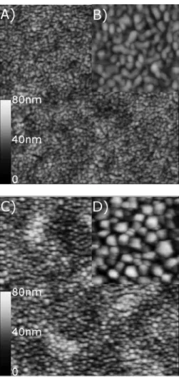
The surface morphology of the films has been investi-gated by AFM and the results for both films are displayed in Fig.2. Figures2共a兲and2共b兲are related to LNO-CF, whereas Figs.2共c兲and2共d兲 correspond to the surface reconstruction of LNO-MW. These images indicate that both films display a smooth, homogeneous, and crack-free surface. Average roughness 共RMS兲 values of ⬃4.3 and 12.4 nm have been obtained from the images of LNO-CF and LNO-MW, respec-tively. The result obtained for LNO-CF is comparable with RMS values of 3.7 nm and 5.5 nm reported in the literature for similar thin films.1,26
The morphology of the grains can be observed in the images with higher magnification, as displayed in Figs.2共b兲 and2共d兲. A comparison between these figures discloses the influence of the heat treatment on the size and shape of the grains of the LaNiO3 films. In fact, elongated grains, with
typical length and width values of 150 and 60 nm, respec-tively, are observed in images belonging to the LNO-CF thin films, whereas those of LNO-MW films exhibit bigger grains with irregular shape and average radius close to 80 nm. Such average values of radius are in line with those of⬃120 nm seen in LaNiO3thin films deposited on LaAlO3substrates.20
We argue that such a difference in the morphologies may be related to the two different process of crystallization em-ployed here. In any event, both methods provided textured films and prolonged times of heat treatment were found to promote grain growth by coalescence and, consequently,
re-sulting in elongated grains and a smoother surface. Similar features have been observed in oriented YBa2Cu3O7 thin
films when subjected to different time intervals during the heat treatment.25
Cross section analyses of these films were performed by SEM and revealed 共not shown兲 that both samples display similar thickness of ⬃200 nm. However, we also mention that a critical thickness⬃50 nm, for depositing LaNiO3thin
films by pulsed laser ablation, has been proposed elsewhere.9 It was argued that films with thickness above this critical value would have cracked surfaces, a feature hardly seen in our thin films.
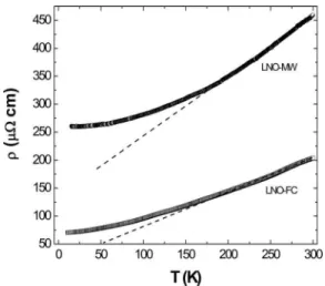
In order to study the transport properties of these thin films, measurements of electrical resistivity共T兲versus tem-perature have been conducted and the relevant results are displayed in Fig. 3. The共T兲curves reveal a monotonic de-crease of共T兲with decreasing temperature, a behavior typi-cally found in metals.1However, a careful inspection of the data indicates that there are at least two different behaviors of共T兲in the temperature range investigated:共a兲at tempera-tures above ⬃100 K, where 共T兲 is linear; and共b兲 at tem-peratures below 100 K, where 共T兲 is larger than expected for a linear behavior. Similar共T兲behaviors have been fre-quently observed in LNO thin films and polycrystalline samples, as discussed elsewhere.1,27,28
FIG. 2. AFM images of the LNO thin films.共a兲and 共b兲Related to the surface reconstruction of the LNO-CF sample and共c兲and共d兲correspond to the LNO-MW thin film.共a兲and共c兲Low magnification共5⫻5 m兲and共b兲 and共d兲high magnification共1⫻1 m兲.
A comparison between LNO-CF and LNO-MW 共T兲 curves revealed a clear difference in the 共T兲 values and, at
T⬍200 K, in the temperature-dependent resistivity data共see Fig. 3兲. In fact, values of at 300 K were found to be 200 ⍀cm and 460 ⍀cm for the films LNO-CF and LNO-MW, respectively. These values of 共T兲 are very low and further indicate that LNO thin films are excellent candi-dates for practical applications. In addition to this, they are in good agreement with 共T= 300 K兲 ⬃300 ⍀cm reported in films of LNO produced by pulsed laser ablation8 and
共T= 300 K兲 ⬃340 ⍀cm in thin films prepared by a sol-gel technique.12 However, these values of 共T= 300 K兲 are much lower than that of ⬃750 ⍀cm obtained for poly-crystalline LNO films grown on Si 共111兲 substrates by the complex polymerization method.1
At low temperatures, or more appropriately at⬃20 K, the values were 72 ⍀cm 共LNO-CF兲 and 259 ⍀cm 共LNO-MW兲. This implies in residual resistivity ratios 共300 K/20 K兲of ⬃2.78 and⬃1.77 for the film crystallized in the conventional furnace and for the film annealed in the microwave oven, respectively. The latter value of
300 K/20 K is essentially the same 共300 K/20 K= 1.75兲 found in LaNiO3 films deposited on SrTiO3 共100兲.27
At temperatures above 200 K, the positive temperature-coefficient of the electrical resistivity, 关共1 /兲d/dT兴, was found to be 3.8⫻10−3 and 3.0⫻10−3 K−1 for LNO-CF and LNO-MW, respectively. These values of 共1 /兲d/dT are comparable to the ones found in ordinary metals like Cu, 共1 /r兲dr/dT⬃4.4⫻10−3 K−1, and other values listed in lit-erature of 2.4⫻10−3 K−1for LaNiO
3.27,28
In order to further discuss the temperature dependence of the共T兲, the temperature ranges were共T兲displays different behaviors were fitted assuming a power law:
共T兲=A+BTn, 共3兲
where A is the residual electrical resistivity, B is the temperature-dependent coefficient, andnranges from 1 to 2. At this point, it is important to notice that the mechanism limiting the mean free path of the carriers in LNO com-pounds is certainly related to the bulk properties and not, e.g., to the grain boundary scattering.29
At higher temperatures, or more appropriately from 200 to 300 K, the 共T兲 curves for both samples were fitted to a linear expression:共T兲=0+AT. Such a behavior of the共T兲
curves is typical of electron-phonon scattering, where 0 is
the residual electrical resistivity of the material andAis the temperature-dependent coefficient. The values of 0 were
⬃35 and ⬃145 ⍀cm for samples CF and LNO-MW, respectively. For the sample heat treated in the conven-tional furnace, the temperature dependence coefficient was 0.55 ⍀cm/ K, whereasA⬃1 ⍀cm/ K was obtained for the sample crystallized in the microwave oven.
By assuming that the linear behavior of 共T兲 data is related to the phonon scattering, the electron-phonon coupling constant can be estimated by using the appropriate expression:30,31
=
បp2
82kBA= 0.246共បP兲
2A, 共4兲
where ប is the Planck constant divided by 2, P is the
plasma frequency,kBis the Boltzmann constant, andAis the
slope of the共T兲curve共⍀cm/ K兲. Assuming that the plas-mon energy បP⬇1 eV, obtained for the LNO bulk when
electron energy-loss experiments are considered,32 the electron-phonon coupling constant can be estimated for both films. The estimated values ofare⬃0.14 for LNO-CF and ⬃0.26 for LNO-MW. These values of are in good agreement with the one of ⬇0.3 found in polycrystalline samples of LaNiO3 共Ref. 28兲 and further suggest a weak coupling between electrons and phonons in this compound.
The lack of saturation of 共T兲 at 300 K for both films indicates that the mean free pathlof the carriers is actually longer than the dimensions of the unit cell. An estimate ofl, at temperatures in which the共T兲data displays a linear be-havior, can be obtained by using the relationship:30,31
l=4.95⫻10
−4 F 共បp兲2
, 共5兲
wherevFis the Fermi velocity, which has been estimated to
be vF⬃1.05⫻107 cm s−1 for LaNiO3,33 andpthe plasma
frequencyបp⬃1 eV. The values ofl, at 300 K, were found
to be⬃31 and⬃15 Å for the LNO-CF and LNO-MW films, respectively. These values oflare much longer than the unit cell parameters obtained through the x-ray data of⬃3.8 Å. In addition to this, the l values are comparable tol⬃15 Å obtained for polycrystalline samples of LaNiO3.29In the case
of the LNO-FC film, the estimatedl is almost twice longer than that reported for the bulk LNO. We argue that such difference inlcan be related to the highly oriented nature of the LNO-FC thin film which results in lower scattering of the charge carriers. It is important to notice that some authors have observed isotropic transport properties of LaNiO3 bulk samples.29
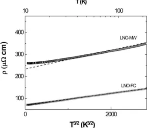
For the LNO-CF thin film, the low temperature共T兲data 共20⬍T⬍140 K兲was found to be well described by Eq.共3兲 with n= 3 / 2, where ACF= 68.7 ⍀cm and BCF
= 0.0271 ⍀cm/ K3/2. The best fit found for the共T兲data is
shown in Fig.4. In Fig.4, it is also shown that the共T兲data of LNO-MW thin film, in the same temperature range, devi-FIG. 3. Temperature dependence of the electrical resistivity of both
samples: LNO-CF and LNO-MW. The dotted lines are guides to the eye.
043708-4 Mambriniet al. J. Appl. Phys.102, 043708共2007兲
ates from theT3/2behavior and seems to obey the expression 共T兲=AMW+BMWT2, as displayed in Fig.5. We were able to
fit the 共T兲 data by using this equation with AMW
= 258.2 ⍀cm and BMW= 0.0023 ⍀cm/ K2. In general,
such a T2 contribution term to 共T兲 is ascribed to the
electron–electron scattering, whereas aT3/2term is related to
a combination of a T2 contribution and an electron-phonon
scattering resistivity T term.1,28 Also, the linear coefficient
BMWis useful to estimate the Kadowaki–Woods ratio共rKW兲 by using rKW⬅BMW/␥2, where ␥ is the electronic specific
heat coefficient. When one assumes ␥⬃13.8 mJ mol−1K−2
for LNO, as reported elsewhere,34 a value of rKW⬃1.2 a0, witha0⬅10 ⍀cm mol2K2J−2, is obtained. As discussed
in Ref.35, the ratiorKWclose toa0indicates strong electron correlations, further suggesting that such electron-electron scattering can be related to the proximity of a nearby Mott transition.
As far as then T-exponent is concerned, we first mention that some authors usually associate the magnitude of this exponent to the presence of defects within grains like oxygen vacancies or even extrinsic grain-boundaries contributions and porosity. However, our samples, based on the discussion made earlier, have similar microstructural features, oxygen stoichiometry, and porosity, and the origin of different values
ofnwould be mainly related to the slight different preferred orientation degree or to the structural strains due to the rapid heat treatment made in the microwave oven. Despite the small differences observed on microstructural and transport properties of these films, the combination of structural, mor-phological, and transport characterizations revealed that the polymeric precursor method allowed to the production of textured single-phase LaNiO3thin films with uniform
micro-structure and excellent electrical properties.
IV. CONCLUSIONS
In summary, textured and single-phase LaNiO3/ SrTiO3
共100兲thin films were successfully produced by the polymeric precursor method. A comparison between the features of these films heat treated in a conventional furnace and in a domestic microwave oven has been made. The XRD analysis indicated a high degree of crystallinity and the structural ori-entation along the共h00兲direction for both films. The surface images obtained by AFM revealed similar roughness values, whereas films LNO-MW have slight smaller average grain size 共⬃80 nm兲 than those observed for LNO-FC 共60–150 nm兲. Electrical resistivity measurements for both films dis-played metallic behavior over the entire temperature range investigated 共20–300 K兲. These measurements also revealed larger electrical resistivity values for LNO-MW films, al-though these differences may be related with both the high heating rate and the low crystallization time used during the heat treatment performed on the microwave oven. Below 150 K, the共T兲curves were fitted by considering different tem-perature dependencies. For the LNO-MW films, the 共T兲 data were fitted with aT2 term; and for the LNO-FC films,
共T兲was adjusted to aT3/2term. The combined results sug-gested that the crystallization processes of LaNiO3thin films in microwave oven, as well as the crystallization in conven-tional furnace are promising routes for producing LNO thin films. In addition to this, the results discussed here make these films promising candidates for application as bottom electrodes in ferroelectric-based memory devices.
ACKNOWLEDGMENTS
The authors acknowledge the financial support from the Brazilian agencies FAPESP, CNPq, and CAPES. One of the authors共R.F.J.兲acknowledges FAPESP under Grant No. 05/ 53241-9 and CNPq under Grant No. 303272/2004-0.
1M. T. Escote, F. M. Pontes, E. R. Leite, J. A. Varela, R. F. Jardim, and E.
Longo, Thin Solid Films445, 54共2003兲.
2M. S. Chen, T. B. Wu, and J. M. Wu, Appl. Phys. Lett.68, 1430共1996兲. 3B. G. Chae, Y. S. Yang, S. H. Lee, M. S. Jang, S. J. Lee, S. H. Kim, W. S.
Baek, and S. C. Kwon, Thin Solid Films410, 107共2002兲.
4C. Guerrero, F. Sánchez, C. Ferrater, J. Roldán, M. V. García-Cuenca, and
M. Varela, Appl. Surf. Sci.168, 219共2000兲. 5A. K. Raychaudhuri, Adv. Phys.44, 21共1995兲.
6P. Lacorre, J. B. Torrance, J. Pannetier, A. I. Nazzal, P. W. Wang, and T. C.
Huang, J. Solid State Chem.91, 225共1991兲.
7N. Wakiya, T. Azuma, K. Shinozaki, and N. Mizutani, Thin Solid Films
410, 114共2002兲.
8F. Sánchez, C. Ferrater, C. Guerrero, M. V. García-Cuenca, and M. Varela,
Appl. Phys. A: Mater. Sci. Process.71, 59共2000兲.
9F. Sánchez, C. Ferrater, X. Alcobé, J. Bassas, M. V. García-Cuenca, and
M. Varela, Thin Solid Films384, 200共2001兲. FIG. 4. T3/2dependence of the electrical resistivity of the sample LNO-CF
and LNO-MW measured in the temperature range 10⬍T⬍200 K.
FIG. 5. T2dependence of the electrical resistivity of the sample LNO-MW measured in the temperature range 10⬍T⬍200 K.
10A. Y. Dobin, K. R. Nikolaev, I. N. Krivorotov, R. M. Wentzcovitch, E. D.
Dahlberg, and A. M. Goldman, Phys. Rev. B68, 113408共2003兲. 11A. Li, C. Ge, P. Lu, and N. Ming, Appl. Phys. Lett.68, 1347共1996兲. 12S. Miyake, S. Fujihara, and T. Kimura, J. Eur. Ceram. Soc. 21, 1525
共2001兲.
13M. T. Escote, F. M. Pontes, E. R. Leite, E. Longo, R. F. Jardim, and P. S.
Pizani, J. Appl. Phys.96, 2186共2004兲.
14F. M. Pontes, E. R. Leite, M. S. J. Nunes, D. S. L. Pontes, E. Longo, R.
Magnani, P. S. Pizani, and J. A. Varela, J. Eur. Ceram. Soc. 24, 2969
共2004兲.
15E. J. H. Lee, F. M. Pontes, E. R. Leite, E. Longo, J. A. Varela, E. B.
Araujo, and J. A. Eiras, J. Mater. Sci. Lett.19, 1457共2000兲.
16F. M. Pontes, E. R. Leite, E. J. H. Lee, E. Longo, and J. A. Varela, J. Eur.
Ceram. Soc.21, 419共2001兲.
17V. Bouquet, M. I. B. Bernardi, S. M. Zanetti, E. R. Leite, E. Longo, J. A.
Varela, M. G. Viry, and A. Perrin, J. Mater. Res.15, 2446共2000兲. 18N. S. L. S. Vasconcelos, J. S. Vasconcelos, V. Bouquet, S. M. Zanetti, E.
R. Leite, E. Longo, L. E. B. Soledade, F. M. Pontes, M. Guilloux-Viry, A. Perrin, M. I. Bernardi, and J. A. Varela, Thin Solid Films436, 213共2003兲. 19J. S. Vasconcelos, N. S. L. S. Vasconcelos, S. M. Zanetti, E. R. Leite, J. A.
Varela, and E. Longo, Appl. Surf. Sci.225, 156共2004兲.
20F. M. Pontes, E. R. Leite, G. P. Mambrini, M. T. Escote, E. Longo, and J.
A. Varela, Appl. Phys. Lett.84, 248共2004兲.
21M. T. Escote, F. M. Pontes, G. P. Mambrini, E. R. Leite, J. A. Varela, and
E. Longo, J. Eur. Ceram. Soc.25, 2341共2005兲.
22T. Ami and M. Suzuki, Mater. Sci. Eng., B54, 84共1998兲.
23W. Lu, P. Zheng, W. Du, and Z. Meng, J. Mater. Sci.: Mater. Electron.15,
739共2004兲.
24K. M. Satyalakshmi, M. Mallya, K. V. Ramanathan, X. D. Wu, B.
Brain-ard, D. C. Gautier, N. Y. Vasanthacharya, and M. S. Hedge, Appl. Phys. Lett.62, 1233共1993兲.
25X. M. Cui, B. W. Tao, J. Xiong, X. Z. Liu, J. Zhu, and Y. R. Li, Physica
C432, 147共2005兲.
26A. Li, D. Wu, Z. Liu, C. Ge, X. Liu, G. Chen, and N. Ming, Thin Solid
Films336, 386共1998兲.
27C. R. Cho, D. A. Payne, and S. L. Cho, Appl. Phys. Lett.71, 3013共1997兲. 28X. Q. Xu, J. L. Peng, Z. Y. Li, H. L. Ju, and R. L. Greene, Phys. Rev. B48,
1112共1993兲.
29N. Gayathri, A. K. Raychaudhuri, X. Q. Xu, J. L. Peng, and R. L. Greene,
J. Phys. Condens. Matter10, 1323共1998兲.
30See, for example, M. T. Escote, V. B. Barbeta, R. F. Jardim, and J. Campo,
J. Phys.: Condens. Matter18, 6117共2006兲; M. T. Escote, V. A. Mesa, R. F.
Jardim, L. Ben-Dor, M. S. Torikachvili, and A. H. Lacerda, Phys. Rev. B
66, 144503共2002兲.
31M. Gurvitch and A. T. Fiory, Phys. Rev. Lett.59, 1337共1987兲. 32J. P. Kemp and P. A. Cox, Solid State Commun.75, 731共1990兲. 33The
vFvalue can be estimated as follows: vF=ប共3n兲1/3/ m*, wheren = 1.7⫻1022 cm−3, by assuming one electron per Ni atom共Ni3+,t
2g
6e
g
1兲 共see
Ref.28兲.
34K. Sreedhar, J. M. Honig, M. Darwin, M. McElfresh, P. M. Shand, J. Xu,
B. C. Crooker, and J. Spalek, Phys. Rev. B46, 6382共1992兲.
35S. Y. Li, L. Taillefer, D. G. Hawthorn, M. A. Tanatar, J. Paglione, M.
Sutherland, R. W. Hill, C. H. Wang, and X. H. Chen, Phys. Rev. Lett.93,
056401共2004兲.
043708-6 Mambriniet al. J. Appl. Phys.102, 043708共2007兲