Modifications in graphene electron states due to a deposited lattice of Au nanoparticles: Density
functional calculations
Sabrina S. Carara,1Ronaldo J. C. Batista,2and Hélio Chacham1,
*
1Departamento de Física, ICEX, Universidade Federal de Minas Gerais, CP 702, 30123-970 Belo Horizonte, MG, Brazil 2Departamento de Física, Universidade Federal de Ouro Preto, Campus Morro do Cruzeiro, 35400-000 Ouro Preto, MG, Brazil
共Received 28 March 2009; revised manuscript received 18 August 2009; published 29 September 2009兲
We perform first-principles investigations of two-dimensional, triangular lattices of Au38nanoparticles de-posited on a graphene layer. We find that lattices of thiolate-covered nanoparticles cause electronic structure modifications in graphene such as minigaps, charge transfer, and new Dirac points, but graphene remains metallic. In contrast, for a moderate coverage of nanoparticles共⬇0.2 nm−2兲, a lattice of bare共noncovered兲Au nanoparticles may induce periodic deformations on the graphene layer leading to the opening of a band gap of a few tens of meV at the Dirac point, in such a way that a properly charged system might become a semiconductor.
DOI:10.1103/PhysRevB.80.115435 PACS number共s兲: 73.22.⫺f, 61.46.Df, 73.90.⫹f
I. INTRODUCTION
The electronic properties of graphene-based materials have been widely investigated since graphene was first syn-thesized in 2004.1Due to graphene’s unique dispersion rela-tion, electrons and holes behave like a two-dimensional共2D兲 gas of massless Dirac fermions, which allows to probe quan-tum electrodynamics phenomena in condensed matter.2–4On the other hand, the metallic共or zero-gap semiconductor兲 na-ture of graphene’s electronic strucna-ture prevents its direct ap-plication as a “bulk” semiconductor material in electronic devices. Several experimental realizations have been made to modify graphene and turn it into a semiconductor, such as cutting or synthesizing graphene in the form of nanoribbons,5 growing graphene epitaxially on SiC,6,7or applying an elec-tric field perpendicular to bilayer graphene.8It has also been suggested that graphene with periodic arrays of antidots9 or BN-graphene bilayers10 might manifest semiconducting be-haviors.
In the present work we investigate, through first-principles calculations, the consequences of depositing a two-dimensional triangular lattice of Au nanoparticles on graphene. Such triangular lattices of functionalized nanopar-ticles can be produced experimentally,11 and the deposition of Au nanoparticles on graphene has already been obtained.12 We find that deposited Au38 nanoparticles that are covered with methylthiolate molecules transfer a net negative charge to graphene and cause electronic structure modifications such as new Dirac-type points and minigaps, but graphene re-mains metallic. In the case of lattices of bare 共noncovered兲 Au nanoparticles, the stronger nanoparticle-graphene interac-tion may lead to the opening of a band gap of a few tens of meV at the graphene Dirac point for moderate concentrations of nanoparticles.
II. METHODOLOGY
We use a first-principles methodology based on the den-sity functional theory13as implemented in theSIESTAcode,14 within the generalized gradient approximation 共GGA兲 共Ref.
15兲and with the use of norm-conserving pseudopotentials.16
For the C, S, and H atoms we employ a basis set consisting of double-zeta radial functions per angular momentum, with the finite range determined by a common confinement energy shift in ␦E= 10−2 Ry 共Ref. 17兲. For Au atoms, we use a different basis set, which is described in previous works.18,19 The real-space grid used for integration was defined by a minimal energy cutoff of 150 Ry共Ref. 20兲in the reciprocal space.
III. RESULTS AND DISCUSSION
A. Deposited layers of functionalized nanoparticles: Band structure near the Fermi level
We first consider two-dimensional arrays of functional-ized Au38nanoparticles deposited on graphene, as shown in Fig. 1. We consider the nanoparticle structure obtained ex-perimentally by Garzonet al.,18where the Au
38metal core is covered by 24 methylthiolate 共CH3S兲 molecules in such a way that the surface gold atoms form quasilinear Au-S-Au bonds, consistent with recent experimental observations.21 We consider two distinct values for the lattice parameteraof the nanoparticle layer, chosen to be commensurate with ei-ther a 9⫻9 共a= 22.43 Å兲 or a 12⫻12 共a= 29.97 Å兲 graphene supercell, as shown in Figs. 1共b兲 and1共c兲. In the first case, the nanoparticle coverage has a density of 0.230 nm−2, and in the second case, 0.129 nm−2. The geom-etries of the Au38 nanoparticle layers and that of the graphene layer were optimized separately, and then as-sembled together at a layer-to-layer distance that minimizes the total energy of the nanoparticle+ graphene system. For both coverage considered, the smallest distance between a hydrogen atom of the functionalized nanoparticle and a car-bon atom of the graphene layer is 2.9 Å at the optimized geometry, which indicates a weak interaction between the nanoparticles and the graphene layer.
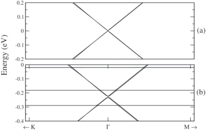
In the upper panel of Fig.2we show the band structure of an isolated 9⫻9 graphene supercell near the Fermi level,22 and in the lower panel we show the band structure of the corresponding nanoparticles+ graphene system shown in Fig.
functionalized Au38film is dispersionless共as it has been pre-viously reported in Ref.23兲. Therefore, the flat bands in Fig.
2共b兲 can be recognized as the electronic states of the nano-particle film. The interaction between the functionalized nanoparticles layer and the graphene layer is too small to lead to a detectable band-gap opening on the共otherwise me-tallic兲 electronic structure of the graphene layer near the ⌫ point, as seen in Fig. 2. Due the differences between the electroaffinities of the functionalized nanoparticles and that of graphene, a net negative charge共of 0.3e/particle兲is trans-ferred from the nanoparticles to the graphene layer. As a result, the energy of the point in k space, where the upper valence band and the lowest conduction band are degenerate 共the Dirac point兲, does not coincide with the Fermi levelEF as in the isolated, neutral graphene 共see upper panel of Fig.
2兲, but it rather shifts downward relative toEF, as shown in the bottom panel of Fig.2共b兲. Apart from the shift inEFdue to this charge transfer, and from minor anticrossing cou-plings on the order of 0.01 eV, at crossing points between the 共flat兲 nanoparticle states and the graphene states, the result-ing band structure of the graphene+ nanoparticles system near the ⌫ point is essentially a superposition of the band
structures of the isolated systems. This is shown in Fig. 2. In Fig. 3共a兲 we show the band structure of an isolated 12⫻12 graphene supercell near the Fermi level, and in Fig. 3共b兲 we show the band structure of the nanoparticles + graphene system commensurate with the 12⫻12 graphene supercell 关shown in Fig. 1共c兲兴. Similar to the case with denser coverage, considered in the previous paragraph, no band gap near the ⌫ point is opened in the functionalized nanoparticles+ graphene system, keeping the metallic charac-ter of the graphene. Also similar to the previous case, the band structure of the nanoparticles+ graphene system near the⌫point is nearly a superposition of the band structures of the isolated systems, and a net negative charge 共of 0.35e/particle兲 is transferred from the nanoparticles to the graphene layer, resulting in an energy shift in the Dirac point relative toEF.
B. Effects of additional charge
We have also investigated the possible changes in the electronic structure of graphene due the inclusion of
addi-(a)
(b)
(c)
FIG. 1. 共Color online兲 共a兲Unit cell of the system composed of Au38共CH3S兲24nanoparticles deposited on graphene, commensurate with a 9⫻9 graphene supercell;共b兲array of those unit cells, shown for the visualization of the nanoparticle lattice; and共c兲array of unit cells that are commensurate with a 12⫻12 graphene supercell.
-0.1 0 0.1
← Κ Γ M→
-0.4 -0.3 -0.2 -0.1
Energy
(eV
) (a)
(b)
FIG. 2. 共a兲Band structure, near the⌫point of a 9⫻9 graphene supercell.共b兲Band structure, near the⌫point of the nanoparticles + graphene system shown in Fig. 1共b兲. In both panels the Fermi level is set to zero and the band structures were calculated along the K-⌫-M directions.
-0.2 -0.1 0 0.1 0.2
← Κ Γ M→
-0.4 -0.3 -0.2 -0.1 0
Energy
(eV)
(a)
(b)
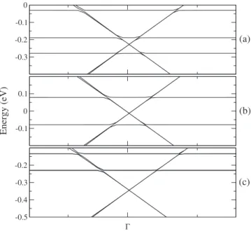
tional charge in the graphene+ nanoparticles system. Figure4
shows the band structures of 共a兲 the neutral 9⫻9 graphene + nanoparticles system,共b兲the system charged with an extra electron, and共c兲the system charged with an extra hole. Upon the addition of an electron 关Fig.4共b兲兴, both the Dirac point and the dispersionless bands of the nanoparticles film are shifted to lower energies, relative to the Fermi energy, by nearly the same amount. This is associated to the fact that the additional negative charge is equally shared between the graphene layer and the nanoparticle film, as indicated by a Mulliken population analysis. The effect of an additional hole in the system is different from that of an additional electron. The extra positive charge is not equally shared be-tween the nanoparticles film and the graphene layer: 70% of the additional positive charge is localized at the nanoparticle. As a result of such asymmetric positive charging, the relative position between the dispersionless nanoparticles bands and the graphene bands are changed due the addition of an extra hole in the system, as it is possible to see in Fig.4共c兲.
As it is also possible to see in panels共b兲and共c兲of Fig.4, the additional electron or hole in the system does not open a band gap on the band structure of the graphene layer near the ⌫ point. This suggests that the long-range nature of the ad-ditional Coulomb potential centered at the nanoparticles is unable to break the A-B sublattice symmetry that makes graphene metallic, or that the metallic screening due to the graphene layer further reduces this symmetry breaking.
C. Effects of an applied electric field
In an another attempt to modify the electronic structure of the nanoparticles+ graphene system, we added a periodic zig-zag potential along the direction perpendicular to the graphene plane, namely,zˆdirection, which corresponds to a
constant external electric field along this direction. We con-sideredEzcomponents of the electric field ranging from −0.5 up to 0.5 V/Å. Figure 5 shows the band structures of the 9⫻9 graphene+ nanoparticles system for Ez= 0, Ez = −0.5 V/Å, and Ez= 0.5 V/Å. Depending on the sign of
Ez, electrical charge is transferred either from graphene to the nanoparticles film 共negative Ez兲, or vice-versa共positive
Ez兲. Concerning the electronic structure, the charge trans-ferred from one part of the system to the other leads to op-posite shifts in the graphenelike bands and of the nanopar-ticlelike bands. However, Fig.5 also shows that the applied field does not open a band gap in the graphenelike electronic states near the ⌫point.
D. New Dirac points and minigaps
Parket al.24have recently predicted that, when a periodic potential with triangular lattice symmetry is applied to graphene, new Dirac points are generated at theM point of -0.3
-0.2 -0.1 0
-0.5 -0.4 -0.3
Energy
(eV)
← Κ Γ M→
0 0.1 0.2 0.3
(a)
(b)
(c)
FIG. 4. Energy bands, near the ⌫ point of the nanoparticles + graphene system shown in Fig.1共b兲 in several charge states:共a兲
uncharged;共b兲charged with an additional electron; and共c兲charged with an additional hole. In all panels, the Fermi level is set to zero and the energy bands are calculated along the K-⌫-M directions.
-0.3 -0.2 -0.1 0
-0.1 0 0.1
Energy
(eV)
Γ -0.5
-0.4 -0.3 -0.2
(a)
(b)
(c)
FIG. 5. Energy bands near the ⌫ point of the nanoparticles + graphene system shown in Fig.1共b兲under applied electrical fields of共a兲Ez= 0,共b兲Ez= −0.5 V/Å, and共c兲Ez= 0.5 V/Å.
← Γ M K
0.7 0.8 0.9 1.0 1.1
Energy
(eV
)
← Γ M K
0.5 0.6 0.7 0.8 0.9
(a) (b)
the system supercell, with anisotropic group velocity. For specific potentials, they also predicted that these new Dirac points can fall in an energy-gap region of the remaining elec-tronic states. Figure 6共b兲 indicates that our proposed 9⫻9 graphene+ nanoparticles system can lead to a new Dirac point at theMpoint, at about 0.7 eV above the Fermi energy 共and at about 0.9 eV above the original graphene Dirac point兲. This results from the folding of the electronic struc-ture of the original graphene layer into the supercell, as seen in Fig. 6共a兲.
The new Dirac point at the M point is anisotropic, as predicted by Park et al.24 To demonstrate that, we consider five distinct linear paths in the first Brillouin zone共BZ兲that start at theMpoint and end, respectively, at the pointsK,K1, K2,K3, and ⌫, as indicated in Fig.7. The band dispersions along those paths, shown in Fig. 8, clearly demonstrate that the feature at theM point has the topology of a Dirac point, and that it is anisotropic, that is, its dispersion depends on the direction on the reciprocal space.
theKpoint. The new Dirac-type point atM almost falls into the minigap region. For the nanoparticles+ graphene system commensurate with the graphene 12⫻12, we also find a similar new Dirac point at M, 0.69 eV above the original Dirac point. The ratio between this value and the correspond-ing value for the 9⫻9 supercell, 0.69/0.92= 0.75, is the same as the inverse of the ratio of the corresponding lattice parameters. This indicates a 1/a scaling of the energy posi-tion of the new Dirac points, relative to the original Dirac point.
E. Deposited layers of bare nanoparticles
As described in the previous paragraphs, the graphene bands are only weakly affected at the⌫point by the interac-tion with methythiolate-capped gold nanoparticles. This is partly due to the relatively large distances between the nano-particle Au cores and the graphene carbon atoms, which leads to a slowly varying perturbing potential on the graphene layer that is unable to break theA-Bgraphene lat-tice symmetry and, therefore, to open a gap on the graphene electronic structure. In an attempt to reduce the Au-carbon distance, we have investigated the interaction of graphene FIG. 7. 共Color online兲Five distinct linear paths in the first BZ
that start at theMpoint and end, respectively, at the pointsK,K1,
K2,K3, and⌫.
← Γ M K
0,3 0,4 0,5 0,6 0,7 0,8 0,9 1
Energy
(eV)
← Γ M K1
0,3 0,4 0,5 0,6 0,7 0,8 0,9 1
← Γ M K2
0,3 0,4 0,5 0,6 0,7 0,8 0,9 1
Energy
(eV)
← Γ M K3
0,3 0,4 0,5 0,6 0,7 0,8 0,9 1
FIG. 8. Energy bands, near the M point of the nanoparticles + graphene system shown in Fig.1共b兲, along the paths indicated in Fig.7.
(a)
(b)
(c)
FIG. 9. 共Color online兲Arrays of 共a兲 6⫻6, 共b兲 9⫻9, and 共c兲
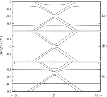
with bare共noncovered兲Au38nanoparticles. In contrast with thiolate-capped Au nanoparticles, which spontaneously as-semble into periodic two-dimensional triangular lattices,11 we do not expect that bare Au nanoparticles on graphene would spontaneously form periodic lattices: a chemical route involving thiol desorption, for instance, might achieve that goal. We note that there are already experimental reports of chemical desorption of thiols from Au nanoparticle films on graphite, leaving thiol-free nanoparticles that do not collapse by sintering.25 Physical deposition routes are also possible. For instance, the physical deposition of small coverage of Au over graphite by molecular-beam epitaxy26 leads to isolated Au clusters, most within a narrow distribution of diameters between 0.5 and 0.7 nm. In our calculations, we first con-sider an amorphous Au38cluster共which is energetically more stable than its ordered octahedral isomer兲18 that is periodi-cally repeated in a triangular lattice that is commensurate with an underlying 9⫻9 graphene supercell关see Fig.9共b兲兴. The geometry of this system was fully optimized until the remaining forces were smaller than 0.05 eV/Å. The opti-mized unit cell and one of its periodic images along the zˆ direction are shown in Fig. 10. As the figure shows, the ge-ometry optimization leads to a strong reduction in the c/a ratio of the supercell, which now represents a periodic Au/ graphene heterostructure along thezˆdirection. The minimal distance between a gold and a carbon atom is⬇2 Å, which indicates a strong interaction between the bare Au nanopar-ticles and graphene, as compared to the weak interaction in the case of the functionalized nanoparticles.
The strong, short-range interaction between the bare gold clusters and the 9⫻9 graphene supercell leads to a band-gap opening of 24 meV near the⌫ point, between the graphene-like bands that previously touched at the Dirac point, as seen in Fig. 11共a兲. The energy-gap region is below the Fermi en-ergy due to electron transfer from the nanoparticles to graphene and, therefore, the neutral system is still metallic. Upon a proper p-doping, however, the Fermi energy can be
placed in the gap region and the graphene+ nanoparticles system would become semiconductor.
To investigate the physical origin of the band gap shown in Fig. 11共a兲, we calculated the band structure of two addi-tional systems. First, we increased thec-axis distance of the supercell such that there are not interactions between peri-odic images along zˆ direction, that is, the system is effec-tively a single-layer graphene plus nanoparticles. The band structure of such system, shown in Fig. 11共c兲, depicts the same band gap as before. Therefore, the origin of the gap is not the interaction between the graphene layers mediated by the nanoparticles. Next, we considered the band structure of a single, isolated graphene layer with the same共slightly兲 dis-torted geometry as in the graphene+ nanoparticles system. FIG. 10. 共Color online兲Unit cell of the system constituted by a
bare Au38nanoparticle deposited on 9⫻9 graphene and one of its periodic images along thezdirection.
-0.3 -0.2 -0.1 0
-0.1 0 0.1
Energy
(eV)
← Κ Γ M→
-0.4 -0.3 -0.2 -0.1
(a)
(b)
(c)
FIG. 11. Energy bands of共a兲 bare Au38nanoparticles confined between successive graphene layers;共b兲the isolated 9⫻9 graphene layer with the same 共distorted兲 geometry as in the previous case; and 共c兲 bare nanoparticles interacting with a single distorted graphene layer.
← Κ Γ M→
-0,4 -0,3 -0,2 -0,1 0
Energy
(eV
)
GGA
← Κ Γ M→
-0,4 -0,3 -0,2 -0,1 0
LDA
(a) (b)
FIG. 12. Energy bands of bare Au38nanoparticles confined be-tween successive graphene layers obtained within either the 共a兲
The band structure of the distorted graphene, shown in Fig.
11共b兲, depicts the same band gap as before. Therefore, the physical origin of the band gap is the breaking of the A-B sublattice symmetry due to the localized distortions in graphene caused by the bare nanoparticles.
The results of Fig.11, indicating the band-gap opening of a specific graphene+ nanoparticles system, were performed with the use of a GGA exchange-correlation functional, as described previously. In order to verify if the band-gap open-ing is related to the use of a specific functional, we per-formed the same calculations within the local-density ap-proximation 共LDA兲 共Ref. 27兲 for the exchange-correlation functional. Figure 12 shows the band structure, near the ⌫ point, of the bare nanoparticles lattice interacting with a 9 ⫻9 graphene supercell obtained within both the GGA and the LDA approximations. Although there are some quantita-tive differences in the band dispersions between the two functional, we obtain the same value of the band gap, of about 24 meV, in both cases.
In order to investigate if the band-gap-opening effect is sensitive to the density of the nanoparticle coverage, we also performed calculations with both larger and smaller graphene supercells. Specifically, we considered lattices of bare, amorphous Au38 clusters commensurate with 12⫻12 and 6⫻6 graphene supercells, shown in Figs.9共c兲and9共a兲, respectively. The geometry of those systems were fully opti-mized until the remaining forces were smaller than 0.05 eV/Å. The minimal distance between a gold and a car-bon atom is about 2 Å in the zˆ direction, similar to the 9 ⫻9 system described in the previous paragraphs. Figure 13共b兲 shows energy bands near the ⌫ point of the 12⫻12 graphene supercell interacting with the commensurate lattice of bare gold clusters, and共a兲shows the corresponding band structure for the isolated graphene system. Unlike the previ-ous result for bare nanoparticles on a 9⫻9 graphene super-cell, in the 12⫻12 system no band gap is opened at⌫due to the nanoparticles, in spite of the fact that there is a deforma-tion in the graphene region below the nanoparticles similar to
the 9⫻9 system. Considering that in the isolated “diluted” limit 共nanoparticles very far apart from each other兲no band gap can be opened due to the semimetallic nature of the graphene host system, a possible explanation for the absence of a band gap in the 12⫻12 system is that such limit has been reached.
The case of the lattice of bare, amorphous Au38 clusters commensurate with the 6⫻6 graphene supercells, shown in Fig. 9共a兲, is structurally distinct from the 9⫻9 and the 12 ⫻12 systems: in this case, the deformation of the graphene layer induced by the nanoparticles is negligible. Consistent with that, the band structure of this system, shown in Fig.
14共b兲, shows that no band gap is opened near the ⌫ point. Therefore, our results suggest that the nanoparticle-induced band-gap opening would only occur for an “intermediate” coverage of nanoparticles, that is, one that leads both to the deformation of the graphene layer and to a significant area of the deformed graphene relative to the undeformed, bulk graphene area between the nanoparticles.
IV. SUMMARY
In summary, we performed a first-principles study of elec-tronic and structural properties of two-dimensional arrays of Au38 nanoparticles, functionalized or not by methylthiolate molecules, in contact with a graphene layer. We find that the interaction of functionalized nanoparticles with the graphene layer causes electronic structure modifications in graphene such as minigaps, charge transfer, and new Dirac points. Nevertheless, this interaction does not lead to the opening of a band gap at the Dirac point, even in the case of charged nanoparticles or under applied electric field. We also find that the interaction of bare nanoparticles with graphene may cause a small band-gap opening at the Dirac point, for a moderate共⬇0.2 nm−2兲 coverage of nanoparticles.
ACKNOWLEDGMENTS
We acknowledge the support from the Brazilian agencies CNPq, CAPES, and FAPEMIG.
-0.2 -0.1 0 0.1
Γ
← Κ M→
-0.3 -0.2 -0.1 0 0.1
Energy
(eV)
(a)
(b)
FIG. 13. Energy bands, near the⌫ point of共a兲 an isolated 12 ⫻12 graphene supercell;共b兲 the system composed of bare, amor-phous Au38clusters and graphene shown in Fig.9共c兲.
-0.2 -0.1 0 0.1
← Κ Γ M→
-0.3 -0.2 -0.1 0 0.1
Energy
(eV
)
(a)
(b)
1K. S. Novoselov, A. K. Geim, S. V. Morozov, D. Jiang, Y.
Zhang, S. V. Dubonos, I. V. Grigorieva, and A. A. Firsov, Sci-ence 306, 666共2004兲.
2K. S. Novoselov, A. K. Geim, S. V. Morozov, D. Jiang, M. I.
Katsnelson, I. V. Grigorieva, S. V. Dubonos, and A. A. Firsov, Nature共London兲 438, 197共2005兲.
3Y. Zhang, Y.-W. Tan, H. L. Stormer, and P. Kim, Nature共
Lon-don兲 438, 201共2005兲.
4K. S. Novoselov, E. McCann, S. V. Morozov, V. I. Fal’ko, M. I.
Katsnelson, U. Zeitler, D. Jiang, F. Schedin, and A. K. Geim, Nat. Phys. 2, 177共2006兲.
5X. Li, X. Wang, L. Zhang, S. Lee, and H. Dai, Science 319,
1229共2008兲.
6S. Y. Zhou, G.-H. Gweon, A. V. Fedorov, P. N. First, W. A. de
Heer, D.-H. Lee1, F. Guinea, A. H. Castro Neto, and A. Lanzara, Nature Mater. 6, 770共2007兲.
7S. Kim, J. Ihm, H. J. Choi, and Y. W. Son, Phys. Rev. Lett. 100,
176802共2008兲.
8J. B. Oostinga, H. B. Heersche, X. Liu, A. F. Morpurgo, and L.
M. K. Vandersypen, Nature Mater. 7, 151共2008兲.
9T. G. Pedersen, C. Flindt, J. Pedersen, N. A. Mortensen, A. P.
Jauho, and K. Pedersen, Phys. Rev. Lett. 100, 136804共2008兲. 10G. Giovannetti, P. A. Khomyakov, G. Brocks, P. J. Kelly, and J.
van den Brink, Phys. Rev. B 76, 073103共2007兲.
11A. Ulman, Chem. Rev.共Washington, D.C.兲 96, 1533共1996兲. 12R. Muszynski, B. Seger, and P. V. Kamat, J. Phys. Chem. C 112,
5263共2008兲.
13W. Kohn and L. J. Sham, Phys. Rev. 140, A1133共1965兲.
14J. M. Soler, E. Artacho, J. D. Gale, A. García, J. Junquera, P.
Ordejón, and D. Sánchez-Portal, J. Phys.: Condens. Matter 14, 2745共2002兲.
15J. P. Perdew, K. Burke, and M. Ernzerhof, Phys. Rev. Lett. 77,
3865共1996兲.
16N. Troullier and J. L. Martins, Phys. Rev. B 43, 1993共1991兲. 17J. Junquera, O. Paz, D. Sanchez-Portal, and E. Artacho, Phys.
Rev. B 64, 235111共2001兲.
18I. L. Garzón, C. Rovira, K. Michaelian, M. R. Beltran, P.
Orde-jon, J. Junquera, D. Sanchez-Portal, E. Artacho, and J. M. Soler, Phys. Rev. Lett. 85, 5250共2000兲.
19R. J. C. Batista, M. S. C. Mazzoni, L. O. Ladeira, and H.
Cha-cham, Phys. Rev. B 72, 085447共2005兲.
20J. Moreno and J. M. Soler, Phys. Rev. B 45, 13891共1992兲. 21P. D. Jadzinsky, G. Calero, C. J. Ackerson, D. A. Bushnell, and
R. D. Kornberg, Science 318, 430共2007兲.
22The Dirac point is at the ⌫point of the 9⫻9 supercell due to
band folding.
23R. J. C. Batista, M. S. C. Mazzoni, I. L. Garzón, M. R. Beltrán,
and H. Chacham, Phys. Rev. Lett. 96, 116802共2006兲. 24C. H. Park, L. Yang, Y. W. Son, M. L. Cohen, and S. G. Louie,
Phys. Rev. Lett. 101, 126804共2008兲.
25D. Grumelli, C. Vericat, G. Benitez, M. E. Vela, R. C.
Salva-rezza, L. J. Giovanetti, J. M. Ramallo-López, F. G. Requejo, A. F. Craievich, and Y. S. Shon, J. Phys. Chem. C 111, 7179
共2007兲.
26Y. Kitsudo, A. Iwamotoa, H. Matsumotoa, K. Mitsuharaa, T.
Nishimuraa, M. Takizawab, T. Akitac, Y. Maedac, and Y. Kido, Surf. Sci. 603, 2108共2009兲.
27D. M. Ceperley and B. J. Alder, Phys. Rev. Lett. 45, 566共1980兲;