Using inelastic scattering of light to understand the nature of electron-phonon interactions and
phonon self-energy renormalizations in graphene materials
Daniela Lopes Mafra
Using inelastic scattering of light to understand the nature of
electron-phonon interactions and phonon self-energy
renormalizations in graphene materials
Daniela Lopes Mafra
Orientador: Prof. Marcos Assun¸c˜ao Pimenta
Tese de doutorado apresentada ao Departamento de F´ısica da Universidade Federal de Minas Gerais como requisito parcial para a obten¸c˜ao do grau de Doutor em F´ısica.
Contents
ABSTRACT iii
RESUMO v
1 Introduction 1
2 Basic properties of monolayer and bilayer graphene 5
2.1 Structure and group theory of graphene . . . 5
2.2 Electronic structure . . . 7
2.2.1 Monolayer graphene . . . 7
2.2.2 Bilayer graphene . . . 8
2.3 Phonon structure . . . 11
2.4 Electron-phonon interaction . . . 13
2.4.1 The Fr¨ohlich Hamiltonian . . . 14
2.4.2 Phonon frequencies and the Kohn anomaly . . . 16
2.4.3 Effects of electron-phonon interaction in monolayer graphene . . . . 20
2.4.4 Effects of electron-phonon interaction in bilayer graphene . . . 22
3 The Raman spectroscopy of graphene 27 3.1 Introduction of Raman Scattering . . . 27
3.2 First order Raman scattering . . . 29
3.3 Second order Raman scattering and the double resonance process . . . 30
3.4 Raman instrumentation . . . 34
4 Graphene and device fabrication 36 4.1 Sample preparation . . . 36
4.1.1 Mechanical exfoliation . . . 37
4.1.3 Metal evaporation . . . 39 4.2 Back gated devices . . . 40 4.3 Top gated devices . . . 43
5 Electron-phonon interactions in graphene 47
5.1 Monolayer graphene . . . 47 5.1.1 Phonon renormalization in the second order Raman processes . . . 48 5.1.2 Electron-phonon coupling of combination modes . . . 54 5.2 Mixing of the optical modes in bilayer graphene . . . 63 5.3 Summary . . . 70
6 Probing the electronic and vibrational structure of bilayer graphene 72 6.1 The historical background . . . 74 6.2 Experimental results . . . 77 6.3 Summary . . . 84
7 Using the G′ Raman Cross-Section To Understand the Phonon
Dynam-ics in Bilayer Graphene Systems 85
7.1 Thermalization effects by emission of low-energy phonons in carbon-systems 86 7.2 Photo-excited electron relaxation in bilayer graphene . . . 87 7.3 Summary . . . 95
8 Conclusions 96
A Publications 99
Abstract
In the last decade, many theoretical and experimental achievements have been made in the physics of graphene. In particular, Raman spectroscopy has been playing an im-portant role in unraveling the properties of graphene systems. In this thesis we use the Raman spectroscopy to study some effects of the electron-phonon coupling in monolayer and bilayer graphene and to probe the electronic and vibrational structure of bilayer graphene. Phonon self-energy corrections have mostly been studied theoretically and ex-perimentally for phonon modes with zone-center (q = 0) wavevectors. Here, we combine Raman spectroscopy and gate voltage to study phonons of monolayer graphene for the features originated from a double-resonant Raman (DRR) process withq ̸= 0 wavevectors. We observe phonon renormalization effects in which there is a softening of the frequency and a broadening of the decay width with increasing the gate voltage, that is opposite from what is observed for the zone-center q= 0 case. We show that this renormalization is a signature for the phonons with q ≈ 2k wavevector that come from both intravalley and intervalley DRR processes. Within this framework, we resolve the identification of the phonon modes contributing to the G⋆ Raman feature, at ∼ 2450 cm−1, and also for
five second order Raman combination modes in the frequency range of 1700−2300 cm−1
of monolayer graphene. By combining the DRR theory with the anomalous phonon renor-malization effect, we show a new technique for using Raman spectroscopy to identify the proper phonon mode assignment for each combination mode.
We also study the behavior of the optical phonon modes in bilayer graphene devices by applying top gate voltage, using Raman scattering. We observe the splitting of the Raman G band as we tune the Fermi level of the sample, which is explained in terms of mixing of the Raman (Eg) and infrared (Eu) phonon modes, due to different doping in the two layers. We show that the comparison between the experiment and theoretical model not only gives information about the total charge concentration in the bilayer graphene device, but also allows to separately quantify the amount of unintentional charge coming from the top and the bottom of the system, and therefore to characterize the intrinsic charges of bilayer graphene with its surrounding environment.
In the second part of this thesis, the dispersion of electrons and phonons near the K point of bilayer graphene was investigated in a resonant Raman study of the G′ band using different laser excitation energies in the near-infrared and visible range.
Slonczewski-Weiss-McClure (SWM) parameters were obtained from the analysis of the dispersive behavior of the G′ band considering both the inner and the outer DRR
pro-cesses. We show that the SWM parameters obtained considering the inner process are in better agreement with those obtained from other experimental techniques, strongly suggesting that the inner process is the main responsible for the G′ feature in graphene.
Additionally, the dependence of the intensity of the four peaks that compose the G′
band of bilayer graphene with laser excitation energy and laser power is explored and ex-plained in terms of the electron-phonon coupling and the relaxation of the photon-excited electron. We show that the carrier relaxation occurs predominantly by emitting a low-energy acoustic phonon and the different combinations of relaxation processes determine the relative intensities of the four peaks that give rise to the G′ band. Some peaks show
Resumo
Na ´ultima d´ecada, muitos avan¸cos te´oricos e experimentais foram alcan¸cados na f´ısica do grafeno. Em particular, a espectroscopia Raman tem sido muito importante para a elucidar propriedades f´ısicas e qu´ımicas em sistemas de grafeno. Nessa tese n´os usamos a espectroscopia Raman para estudar alguns dos efeitos do acoplamento el´etron-fˆonon no grafeno de camada ´unica e de dupla camada, e para se obter informa¸c˜oes sobre a estrutura eletrˆonica e vibracional do grafeno de camada dupla. As renormaliza¸c˜oes das energias dos fˆonons tem sido estudadas basicamente para fˆonons com vetor de onda nulo (q= 0). Aqui, n´os combinamos a espectroscopia Raman com aplica¸c˜ao de tens˜ao de porta para estudar, em grafeno de camada ´unica, as bandas originadas do processo Raman com dupla ressonˆancia (DRR) com vetores de onda q ̸= 0. N´os observamos os efeitos de renormaliza¸c˜ao dos fˆonons, em que h´a a diminui¸c˜ao da frequˆencia e o alargamento no decaimento dos fˆonons com o aumento da tens˜ao de porta, e esse efeito ´e o oposto do que ´e observado para os fˆonons com q = 0. N´os mostramos que esse tipo de renormaliza¸c˜ao observada ´e uma assinatura dos fˆonons com vetor de ondaq ≈2kque vˆem de um processo DRR intervale ou intravale. Dentro desse contexto, n´os identificamos, para o grafeno de camada ´unica, os modos de fˆonons que contribuem para a banda Raman G⋆, em
∼ 2450 cm−1, e para outros cinco picos provenientes de combina¸c˜ao de modos na regi˜ao
de frequˆencia 1700−2300 cm−1. Combinando a teoria do processo DRR com o efeito de
renormaliza¸c˜ao de fˆonons, n´os mostramos uma nova t´ecnica para usar a espectroscopia Raman para identificar cada modo Raman apropriadamente.
N´os tamb´em estudamos o comportamento dos modos ´opticos do grafeno de camada dupla combinando-se o espalhamento Raman e a aplica¸c˜ao de tens˜ao de porta em dispos-itivos desse material. N´os observamos que a banda G se divide em duas quando o n´ıvel de Fermi da amostra ´e mudado, e isso ´e explicado em termos da mistura dos modos de fˆonon Raman (Eg) e infravermelho (Eu) devido a diferen¸ca de concentra¸c˜ao de carga nas duas camadas. N´os mostramos que a compara¸c˜ao entre os dados experimentais e o modelo te´orico n˜ao d´a apenas informa¸c˜ao sobre a concentra¸c˜ao de carga total no dispositivo de grafeno de camada dupla, mas tamb´em nos permite quantificar separadamente as cargas n˜ao intencionais provenientes da camada de cima e de baixo do sistema, e, portanto, caracterizar a intera¸c˜ao do grafeno de camada dupla com o ambiente em sua volta.
Na segunda parte dessa tese, a dispers˜ao de el´etrons e fˆonons perto do ponto
v´arias energias de excita¸c˜ao de laser na regi˜ao do infravermelho e do vis´ıvel. A estru-tura eletrˆonica foi analisada dentro da aproxima¸c˜ao de liga¸c˜oes-forte, e os parˆametros Slonczewski-Weiss-McClure (SWM) foram obtidos atrav´es do comportamento dispersivo da banda G′ considerando-se tanto o processo DRR interno quanto o externo. N´os
mostramos que os parˆametros SWM obtidos considerando-se o processo DRR interno est´a em melhor acordo com os valores obtidos por outras t´ecnicas experimentais, sug-erindo fortemente que o processo interno ´e o principal respons´avel pela banda G′ no grafeno.
Al´em disso, a dependˆencia da intensidade dos quatro picos que comp˜oe a banda G′
do grafeno de camada dupla com a energia de excita¸c˜ao de laser e com a potˆencia do laser ´e explorada e explicada em termos do acoplamento el´etron-fˆonon e do relaxamento dos el´etrons foto-excitados. N´os mostramos que o relaxamento dos el´etrons ocorre predomi-nantemente pela emiss˜ao de fˆonons ac´usticos de baixa energia e as diferentes combina¸c˜oes dos processos de relaxamento determinam as intensidades relativas dos quatro picos que d˜ao origem `a banda G′. Esse efeito nos fornece informa¸c˜oes importantes sobre a dinˆamica
Chapter 1
Introduction
Why phonon and electron-phonon interactions matters? This question is undoubtable the start-point to understand many fundamental phenomena in solids. Phonon is the name given to a quantum of energy of traveling vibrational wave in a solid. Because the interatomic forces in a solid are so strong, there is little profit in considering the motion of an atom in a crystal in terms of particle motion. Any momentum we might give to one atom is so quickly transmitted to its neighbors that after a very short time it would be difficult to tell which atom we had initially displaced. But we do know that a vibrational wave in the solid will exist for a much longer time before it is attenuated, and is therefore a much more useful picture of an excitation in the material. Since a vibrational wave is specified by giving the coordinates not of just one atom but of every atom in the solid, we call this a collective motion. A phonon is thus an example of a collective excitation in a solid [1].
hinders the movements of the charge, thus decreasing its mobility [1].
Another fundamental consequence of the electron-phonon interactions is the super-conductivity phenomenon. In this case, there is an effective electron-electron interaction mediated by phonons, that allow pairs of electrons to form a bound state of lower energy than that of the two free electrons (in other words, phonons that before were scattering electrons apart throughout the material are now helping the electrons to be stuck together. This means less resistance and better conductivity!). The existence of these bound state of two electrons with opposite wavenumber and spin, known as Cooper pairs, provides the foundation for the theory of superconductivity [1]. Additionally, the Peierls transition, in which the dimerization of the lattice occurs to minimize the system energy, and the Kohn anomaly, an abrupt softening of the phonon energy characterized by the disconti-nuity of the derivative of the phonon frequency, are also fenomena directly related to the electron-phonon coupling. By now, the reader probably has the answer to the question asked earlier and should be convinced of the importance of phonons and electron-phonon interactions in a system.
Electron-phonon interactions can be observed in a diversity of materials. Here, this thesis is mainly devoted to the study of electron-phonon interactions, as well as their con-sequences, in graphene-like systems, which have been shown as ideal platforms to observe some of the effects mentioned above. Graphene is a special material due to its fascinating electrical, mechanical, optical and thermal properties [2–5]. This strictly two-dimensional material exhibits exceptionally high crystal and electronic quality, in which charge carriers can travel thousands of interatomic distances without scattering [5,6], and has revealed a bunch of new physics and potential technological applications. Particular interest has been turned to monolayer graphene due to the unique nature of its charge carriers, that make it a promisor material for photonics, optoelectronics and organic electronics such as in solar cells, light-emitting, touch screen and photodetctors devices [2,7,8]. Some progress in the application of graphene is already done, as illustrated in Fig. 1.1. In con-densed matter physics, most of materials are ruled by the Schr¨odinger equation, usually being quite sufficient to describe electronic properties of materials. Monolayer graphene is an exception and its charge carriers mimic relativistic particles and are more easily and naturally described starting with the Dirac equation [9]. The electronic structure of monolayer graphene has a linear dispersion around the K point of the Brillouin zone and it is a zero gap semiconductor.
Figure 1.1: (a) Electrons pass through graphene with less resistance than through silicon, making the carbon sheet a good candidate for future chips [12]. (b) Hybrid graphene-quantum dot phototransistors with ultrahigh gain [13]. (c) Light-emitting Electrochemical cell [14]. (d) A transparent ultralarge-area graphene film transferred on a 35-inch PET sheet [8]. (e) A graphene-based touch-screen panel connected to a computer with control software [8]. (f) Graphene nanopore for DNA sequencing [15].
graphene is also a zero gap semiconductor, it is a highly desired material for the develop-ment of graphene-based electronics such as field effect transistor [5,6], since it becomes a tunable band gap semiconductor under the application of an electric field perpendicular to the system [10,11]. However, for all the desirable applications of graphene, it is extremely important to understand all the properties of these materials.
non-destructive technique.
Traditionally, electron-phonon interactions are investigated through chemical dop-ing, in which the charge carrier density is varied by the introduction of impurities [19]. However, the appliance of electrical fields to control carriers in materials (so-called the electrical field effect) is an alternative method for changing the charge carrier density effectively in low dimensional systems. In this thesis we combine both the electric field effect and Raman spectroscopy to study the electron-phonon coupling in graphene-like systems. Also, a structural study of the bilayer graphene is done by the analysis of the double resonance Raman band known as G′ (or 2D) band.
Chapter 2
Basic properties of monolayer and
bilayer graphene
This chapter brings an overview of the electronic and vibrational structures of graphene. A special focus will be given to the electron-phonon interactions in the last sec-tion. In particular, some important consequences of these interactions in the frequency and line width of the zone-center phonons for monolayer and bilayer graphene will be given.
2.1
Structure and group theory of graphene
Graphene is a flat layer of carbon atoms in a honeycomb lattice withsp2
hybridiza-tion. Fig. 2.1(a) shows the hexagonal real space for the monolayer graphene with two inequivalent atoms in the unit cell and the unit cell lattice vectors a1 and a2, given by:
a1 =
a 2(
√
3ˆx+ ˆy), (2.1)
a2 =
a 2(−
√
3ˆx+ ˆy), (2.2)
Figure 2.1: (a) The real space of monolayer graphene showing the non-equivalent A and B atoms and the primitive lattice vectors a1 and a2. (b) The real space top-view of bilayer graphene. Black dots plus black open circles, and red dots represent the atoms in the lower and upper layers, respectively. (c) The three dimensional unit cells of bilayer graphene. (d) The reciprocal space for both monolayer and bilayer graphene showing the first Brillouin zone in light gray, the high symmetry points and the two reciprocal vectors b1 and b2.
graphene is shown in Fig. 2.1(d) highlighting the high symmetry points Γ, K, K′,M and
the high symmetry linesT,T′ andΣ. Any other generic point outside the high symmetry
points is named hereu. Since there is no periodicity in the ˆˆzcartesian direction for bilayer graphene, its reciprocal space is the same of monolayer graphene. The reciprocal vector b1 and b2 are given by:
b1 =
2π a (
√
3
3 kxˆ + ˆky), (2.3)
b2 =
2π a (−
√
3
3 kxˆ + ˆky). (2.4)
Group theory is a powerful theoretical tool to determine eigenvectors, the number and the degeneracies of eigenvalues and to obtain and understand the selection rules gov-erning, for example, electron-radiation and electron-phonon interactions. The monolayer graphene on an isotropic medium has the space group P6/mmm (D1
Table 2.1: The space groups and wavevector point groups for monolayer graphene, N-layer graphene and graphite (N infinite) at all points in the BZ.
Space group Γ K (K′) M T (T′) Σ u
Monolayer P6/mmm D6h D3h D2h C2v C2v C1h
N even P3m1 D3d D3 C2h C2 C1v C1
N odd P6m2 D3h C3h C2v C1h C2v C1h
N infinite P63/mmc D6h D3h D2h C2v C2v C1h
2.2
Electronic structure
2.2.1
Monolayer graphene
The atomic orbitals in graphene are in a sp2 hybridization, in which the carbon
atoms are bounded covalently to each other forming a 120o angle. There are three in-plane σ orbitals and one out-of-plane π orbital. Since the π electrons are less bounded to the atoms, they can move in the crystal and can be excited to the conduction band more easily than the σ electrons, giving rise to interesting electronic and optical physics phenomena.
The electronic structure of graphene can be described by tight-binding calculations considering interactions with just first neighbors [20]. The problem consists of solving the Schr¨odinger equation,
Ej(k) = ⟨
ψj|H|ψj⟩
⟨ψj|ψj⟩ , (2.5)
where ψi and ψj are the Bloch’s functions given by: ψk(r) =
∑
j
cj(k)φkj(r), (2.6)
where φkj(r) is given by:
φkj(r) = 1
√
M ∑
l
eik.R(l)ϕl(R(l)
−r). (2.7)
M is the number of unit cells, R(l) is the vector giving the position of an atom in the j-th unit cell and ϕl is the l-th atomic orbital of the atom. It follows that the electronic dispersion of monolayer graphene is given by
E±(k) =
ϵ2p±γ0f(k)
'
M
K
K
G
2010 15
5
0
-5
-10
p
*
p
Figure 2.2: The graphene’s π and π∗ electronic dispersion calculated over the first
Bril-louin zone. The inset shows the dispersion along the high-symmetry points. The values used forγ0 and s are, respectively, 3.033 eV and 0.129 eV. [20] The zoom shows the linear
dispersion near the K point.
where γ0 parameter is the nearest neighbor transfer integral between the atomic orbitals
of the carbon atoms A and B of the graphene sheet, s is the overlap integral and the function f(k) is given by
f(k) = √
1 + 4 cos
√
3kxa 2 cos
kya
2 + 4 cos
2 kya
2 . (2.9)
Eq. 2.8 is plotted as a function ofk, as exhibited in the Fig. 2.2. Monolayer graphene is a zero gap semiconductor, where the valence π and conduction π⋆ bands touch each other at the K (or Dirac) point, and this is where the Fermi level is located. We can expand Eq. 2.8 (considering ϵ2p and s equal zero) for values of kclose to the K point. In this case, the electronic dispersion of monolayer graphene is given by [20]
E(k) =~vFk (2.10)
where vF =
√
3γ0a/2~ is the Fermi velocity of the electrons near the Dirac point and is
close to 1×10⁶m/s [5]. We can see that around the K point, the electronic structure can
be described as a linear dispersion (see the zoom of Fig. 2.2).
2.2.2
Bilayer graphene
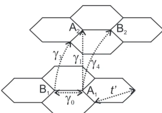
Figure 2.3: The intra- (γ0 and t′) and inter-layer (γ1, γ3 and γ4) tight-binding hoping
parameters in bilayer graphene.
(SWM) parametrization [22,23], using the nearest-neighbor hopping parametersγ0,γ1,γ3
andγ4 (shown in Fig. 2.3). The parameter ∆, which represents the difference between the
on-site energies of the two layers, and t′, which is the in-plane second-neighbor hopping
parameter, can also be included. The electronic structure of bilayer graphene is then, given by solving the 4×4 tight-binding Hamiltonian [24]
Hbilayer =
∆ γ0f(k) γ1 γ4f∗(k)
γ0f∗(k) 0 γ4f∗(k) γ3f(k)
γ1 γ4f(k) ∆ γ0f∗(k)
γ4f(k) γ3f∗(k) γ0f(k) 0
(2.11)
Solving the Hamiltonian, we find two valence bands (π1 andπ2) and two conduction
bands (π⋆
1 and π2⋆). Bilayer graphene is also a zero gap semiconductor but the electronic
dispersion is no longer linear around theKpoint, but it has a hyperbolic dependence with k, as can be seen in Fig. 2.4 [24]. One valence band touch one conduction band at the K
point and the other two bands have a gap of 2γ1. Considering only theγ0 andγ1 hopping
parameters, the solution for the Hamiltonian can be simplified to [25]
E(k) = s [
±γ21 + √
γ2k2+γ 2 1
4 ]
, (2.12)
where s is a band index: +1 for conduction band and −1 for valence band, and γ =
√
3γ0a/2.
Theγ3 andγ4 parameters have interesting consequences in the electronic structure.
γ3gives rise to a trigonal warping effect in the low energy spectrum, where the equienergies
curves have triangular shape, whileγ4 is related to the electron-hole asymmetry in bilayer
0 4 8 -4 -8 -12
M
G
K
M
p
2
p
1
Figure 2.4: Electronic structure of bilayer graphene along the high symmetry lines cal-culated by Partoens and Peeters [24]. The zoom shows the hyperbolic dispersion near the
K point.
Including theγ3andγ4parameters (∆ andt′were also included), along the high symmetric
line ΓKM direction the 4×4 matrix factorizes, and the dispersion of the four electronic bands are given by [18]:
Eπ1∗ π2 = −
γ1 −σv3+ ∆′±ξ1
2 , (2.13)
Eπ∗2 π1 =
γ1+σv3+ ∆′±ξ2
2 , (2.14)
where vi =γi/γ0,
∆′ = ∆ +t′ [ 2 cos ( 2π 3 − √ 3kacc 2 ) + cos ( 4π 3 − √ 3kacc )] , (2.15)
ξ12 =
√
(γ1+v3σ±∆′)2+ 4((1∓v4)2σ2∓σv3(∆′ ±γ1)), (2.16)
and
σ=γ0
[ 2 cos ( 2π 3 − √ 3kacc 2 ) + 1 ] . (2.17)
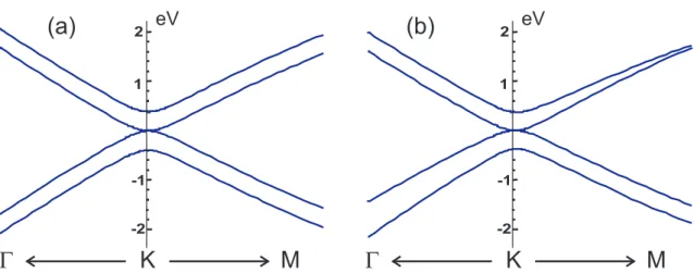
Figure 2.5: Electronic structure of bilayer graphene around the K point using (a)γ3 and
γ4 equal to zero and (b) γ3 and γ4 hopping parameters different from zero (γ3 = 0.3 eV
and γ4 = 0.15 eV).
creates an asymmetry between the two layers that lowers the whole symmetry of the bilayer system, consequently opening an electronic band gap at the K point.
2.3
Phonon structure
As shown in Section 2.1, the monolayer graphene sheet has two atoms per unit cell, each one with three degrees of freedom, thus having 6 phonon branches. There are three acoustic (A) branches, with frequencyω = 0 at theΓ point, and three optic (O) branches. Also, the phonon modes are classified as longitudinal (L) or transverse (T) according to vibrations parallel or perpendicular to the carbon-carbon bond directions, respectively. The transverse modes can be in-plane (i) or out-of-plane (o) and the longitudinal modes are always in-plane.
These phonon branches can be calculated by using a simple harmonic oscillator model which lead us to solve the equation
Miu¨i = n ∑
j
Kij(ui−uj) (i= 1, ..., N), (2.18)
(b)
(a)
Figure 2.6: (a) Phonon dispersion of graphene over the entire Brillouin zone calculated by force constants method [20]. (b) Phonon dispersion of monolayer graphene in the high symmetric directions calculated by Popov and Lambin [27] using the tight-biding method. The phonon branches are labeled: out-of-plane transverse acoustic (oTA); in-plane transverse acoustic (iTA); longitudinal acoustic (LA); out-of-in-plane transverse optic (oTO); in-plane transverse optic (iTO); longitudinal optic (LO).
phonon dispersion in the high symmetric directions calculated by Popov and Lambin [27] using the tight-binding approach.
At the Γ point of monolayer graphene, the iTO and LO modes are double degener-ated and correspond to the vibrations of the sublattice A against the sublattice B as shown in Fig. 2.7. According to group theory, the degenerated zone-center LO and iTO phonon modes belong to the two-dimensional representation E2g, which is Raman active [20].
This mode can be seen in the Raman spectrum with frequency around 1582 cm−1 and it
is known as the G band. The G band is one of the most prominent feature in the Raman spectrum of graphene, as shown in Section 3.2.
For bilayer graphene, there are four atoms in the unit cell, and then, each phonon branch of monolayer graphene splits into two branches. The E2g phonon mode of mono-layer graphene splits into two double degenerated modes associated with the in-phase (IP) and out-of-phase (OP) displacements of the atoms in the two layers, that belong to the representations Eg and Eu of the D3d point group, respectively [28]. The Eu mode is observable in the Infrared spectroscopy, while the Eg mode can be seen as one peak in the Raman spectrum (G band).
Figure 2.7: Vibrations of the two atoms of the unit cell of monolayer graphene that correspond to the six phonon branches at the Γ point. The double degenerated modes LO and iTO gives rise to the G band in the Raman spectrum.
the dispersion of the phonon modes. This is the case in graphene for the LO and iTO phonon branches around the Γ and K points, respectively. In these points, there is a strong electron-phonon coupling and a more carefull calculation must be done in order to correctly describe the behavior of the phonon modes. More details about the electron-phonon coupling will be given in the next section.
2.4
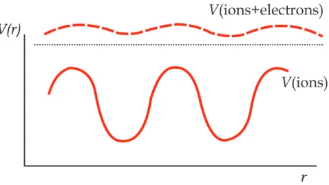
Electron-phonon interaction
Figure 2.8: The deep potential due to the displacement of the ions by a phonon is screened by the flow of electrons.
with electrons.
2.4.1
The Fr¨
ohlich Hamiltonian
In this model we take for granted the concept of screening, and assume that the ions interact with each other and with the electrons only through a short-range screened potential (dashed line in Fig. 2.8), and we treat the electrons themselves as independent fermions. Also we neglect electron-electron interactions. For a Bravais lattice our unper-turbed Hamiltonian, where the electrons and phonons are treated separately, is:
H0 =
∑
k
εkc†kck+ ∑
q,s
~ωq,sa†
q,saq,s, (2.19)
where c†k (ck) is the creation (annihilation) operator for the electrons with energy εk and momentum k, and a†
q (aq) is the creation (annihilation) operator for the phonons with energy ~ωq, momentum q and direction of polarizations. If it happens that s is parallel
to q, we say that it is a longitudinally polarized phonons in the crystal. If s·q= 0, the phonon is transversely polarized. To the unperturbed Hamiltonian, we add the interaction H1 of the electrons with the screened ions:
H1 =
∑
k,k′,l
⟨k|V(r−l−yl)|k′⟩c†kck′, (2.20)
distance from the center of the ion, whereyl is the ion displacement from the equilibrium position l. We can use the Fourier transform of the potencial, then:
Vk−k′ = Ω−1
∫
ei(k′−k)·(l+y
l) V(r−l−y
l)d(l+yl) (2.21) where Ω is the crystal volume, and we can rewrite Eq. 2.20 as:
H1 =
∑
k,k′,l
ei(k′−k)·(l+yl) V
k−k′ c†kck′. (2.22)
If we assume that the displacementyl of the ion is sufficiently small that (k′−k)·yl ≪1, we have:
ei(k′−k)·yl ≃ 1 +i(k′−k)·y
l (2.23)
= 1 +iN−1/2(k′ −k)·∑ q
eiq·l y
q, (2.24)
whereq=k−k′. Substituting Eq. 2.24 into Eq. 2.22, we can separate H1 into two parts,
H1 =HBloch+Hel−ph. The first term HBloch = ∑
k,k′,l
ei(k′−k)·l
Vk−k′ c†kck′ (2.25)
is independent of the lattice displacements. The second term can be written as:
Hel−ph = iN−1/2 ∑
k,k′,l,q
ei(k′−k+q)·l
(k′−k)·y
q Vk−k′ c†kck (2.26)
= iN1/2∑ k,k′
(k′−k)·yk−k′ Vk−k′ c†kck′. (2.27)
The displacement yq can be written in the harmonic approximation as a function of the phonon creation and annihilation operators as:
yq= ∑
s √
~
2M ωq,s
(a†−q,s+aq,s)s. (2.28)
The Hel−ph then becomes:
Hel−ph=i ∑
k,k′,s
√
N~
2M ωk−k′,s
(k′−k)·sV
k−k′ (a†k′−k,s+ak−k′,s) c†kck′. (2.29)
k’ k -q(=k’-k) (a) k’ k q(=k-k’) (b)
Figure 2.9: The Fr¨ohlich Hamiltonian includes an interaction term in which an electron is scattered from k′ to k with either (a) emission or (b) absorption of a phonon. In each case the total momentum is conserved.
for whichsis parallel to k′ −k, will enter Hel−ph. Also, since theHBloch is not dependent
of the displacement, we shall neglect its effects for the electron-phonon interaction. With these simplifications we are left with theFr¨ohlich Hamiltonian:
H =∑ k
εkc†kck+ ∑
q
~ωqa†
qaq+ ∑
k,k′
Mk,k′ (a†−q+aq) c†kck′, (2.30)
where the electron-phonon matrix element is defined by:
Mk,k′ =i
√ N~
2M ωq |
k′ −k| Vk−k′. (2.31)
The interaction Hel−ph can be considered as being composed of two parts - terms involving a†−qc
†
kck′ and terms involving aqc †
kck′. These terms may be represented by the diagrams shown in Figs. 2.9(a) and (b), respectively. In the first diagram an electron is scattered from k′ to k with the emission of a phonon with momentum (k′−k). The
second diagram represents the electron being scattered from k′ to k with the absorption of a phonon with momentum (k−k′).
2.4.2
Phonon frequencies and the Kohn anomaly
To calculate the effect of the electron-phonon interaction on the phonon spectrum, we may use perturbation theory to calculate the total energy ε of the system described by the Fr¨ohlich Hamiltonian (Eq. 2.30) to second order in Hel−ph:
ε=ε0+⟨Φ|Hel−ph|Φ⟩+ ⟨
Φ|Hel−ph(ε0−H0)−1Hel−ph|Φ ⟩
, (2.32)
(a) k’ k -q (b) k’ k k q -q
Figure 2.10: The Fr¨ohlich Hamiltonian includes an interaction term in which an electron is scattered from k′ to k with either (a) emission or (b) absorption of a phonon. In each case the total momentum is conserved.
Φ. In second order there is a set of nonvanishing terms, as the phonon destroyed by the first factor of Hel−ph to act on Φ can be replaced by the second factor ofHel−ph, and vice
versa. We then find the contribution of the second-order terms ε2 to be
ε2 =⟨Φ|
∑
k,k′
Mk,k′(a†−q+aq) c†kck′(ε0−H0)−1 ×
∑
k′′,k′′′
Mk′′,k′′′(a†−q′+aq′)c†k′′ck′′′|Φ⟩
(2.33)
=⟨Φ|∑ k,k′
|Mk,k′|2
[
(a†−qa−q)ck†ck′ c†k′ck (ε0−H0)
+ (aqa
† q)c
† kck′ c
† k′ck
(ε0−H0)
]
|Φ⟩, (2.34)
all other terms having zero matrix element since the resulting wavefunction will be orthog-onal to Φ. The first term in the brackets in Eq. 2.34 can be represented as in Fig. 2.10(a). An electron is first scattered fromktok′with the absorption of a phonon with momentum
−q=k′−k. The factor (ε0−H0)−1 measures the amount of time the electron is allowed
by the Uncertainty Principle to stay in the intermediate state k′ and can be written as the energy difference between the initial and intermediate states, (εk+~ω−0q−εk′)−1. The
electron is then scattered back into its original state with the re-emission of the phonon. We can represent the second term in Eq. 2.34 by Fig. 2.10(b), and then, we find an energy denominator ofεk−~ω0q−εk′.
We can write the creation and annihilation operators in terms of occupation numbers (nk ornq). For fermions (electrons) we have:
c†kck = nk (2.35)
ckc†k = 1−nk, (2.36)
and for bosons (phonons):
a†qaq = nq (2.37)
Rearranging the creation and annihilation operators in Eq. 2.34 into the form of number operators then gives:
ε2 =⟨Φ|
∑
k,k′
|Mk,k′|2
[
n−q c†kck(1−nk′)
(εk−εk′ +~ω0−q)
+(1 +nq)c
†
kck(1−nk′)
(εk−εk′ −~ωq0)
]
|Φ⟩ (2.39)
=⟨Φ|∑ k,k′
|Mk,k′|2
[
n−qnk(1−nk′)
(εk−εk′+~ω0−q)
+(1 +nq)nk(1−nk′) (εk−εk′ −~ωq0)
]
|Φ⟩. (2.40)
It may be assumed that ωq = ω−q, and hence that in equilibrium ⟨nq⟩ = ⟨n−q⟩. Also,
⟨nqnknk′⟩= 0 by symmetry. Then:
ε2 =
∑
k,k′
|Mk,k′|2
⟨nqnk⟩(εk−εk′ −~ω0q) + (⟨nk⟩ − ⟨nknk′⟩+⟨nqnk⟩)(εk−εk′ +~ωq0)
(εk−εk′)2−(~ωq0)2
(2.41)
=∑
k,k′
|Mk,k′|2
2⟨nqnk⟩(εk−εk′) + (⟨nk⟩ − ⟨nknk′⟩)(εk−εk′+~ω0q)
(εk−εk′)2−(~ωq0)2
. (2.42)
The total energy of the system is then given by:
ε=~ωq0⟨nq⟩+∑
k,k′
|Mk,k′|2 ⟨nk⟩
[
2⟨nq⟩(εk−εk′)
(εk−εk′)2−(~ωq0)2
+ 1− ⟨nk′⟩ (εk−εk′ −~ωq0)
]
. (2.43)
The effect of the electron-phonon interaction on the phonon spectrum is contained in the term proportional to ⟨nq⟩ in Eq. 2.43. Now the perturbed phonon energy ~ωqp is the energy required to increase ⟨nq⟩ by unit
~ωqp = ∂ε
∂⟨nq⟩
=~ω0q+∑
k
|Mk,k′|2
2⟨nk⟩(εk−εk′)
(εk−εk′)2−(~ωq0)2
. (2.44)
If we neglect the phonon energy in the denominator in comparison with the electron energies we have
~ωp
q=~ω0q− ∑
k
2|Mk,k′|2 ⟨nk⟩(εk′ −εk)−1. (2.45)
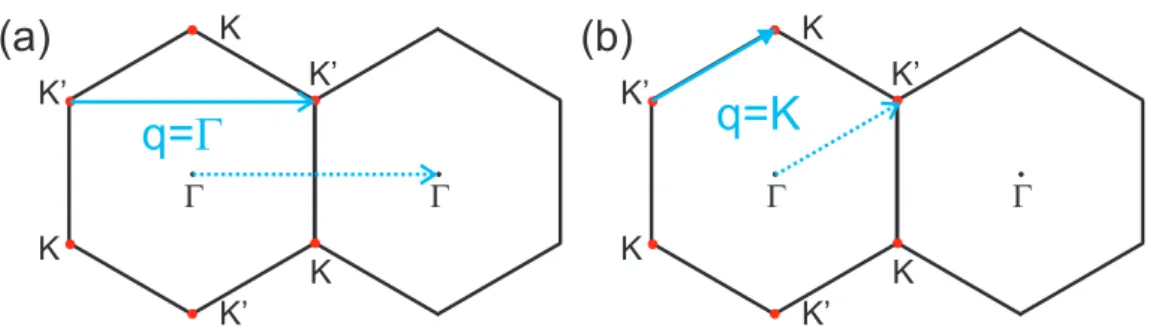
G K K’ K K K’ K’ G G K K’ K K K’ K’ G
q=
G
q=K
(a)
(b)
Figure 2.11: The two possible vector (a) q = Γ and (b) q = K that can connect two electronic states in the Fermi surface (red dots) in graphene.
are connected by q in the same Fermi surface. Evaluating ∂~ωqp/∂q and neglecting the
variation of Mk,k′ with q, the electron-phonon interaction contributes an amount
2∑ k
|Mk,k′|2 ⟨nk⟩(εk−q−εk)−2
∂εk−q
∂q . (2.46)
Here, εk =~2|k|2/2m, εk−q = ~2|k−q|2/2m and |k−q|2| =k·k−2k·q+q·q. For simplicity, we can suppose that qis in the x-direction, so
(εk−q−εk) =
~2
2m(−2kxqx+q
2
x) = −
~2
mqx(2kx−qx). (2.47) The differential in Eq. 2.46 is given by
∂εk−q ∂qx
=− ~
2
2m(2kx−2qx). (2.48)
Substituting Eqs. 2.47 and 2.48 into Eq. 2.46, we have
2∑ k
|Mk,k−q|2 ⟨nk⟩ [
−~2
2mqx(2kx−qx) ]−2
−~2
2m (2kx−2qx) (2.49)
=2∑ k
|Mk,k−q|2 ⟨nk⟩ 1 ~2 q2 x 2m [
(2kx−qx)−qx (2kx−qx)2
]
=2 kF
∑
k=0
|Mk,k−q|2 ⟨nk⟩ 1
~2q2
x
2m [
1
(2kx−qx) −
qx (2kx−qx)2
]
. (2.50)
When the summation is performed, we can see that the first term in Eq. 2.50 cause a logarithmic divergence, and thus a kink in the phonon dispersion is observed. This divergence when q= 2kF is the so-called Kohn anomaly [1].
q=Γ and forq=K, as shown in Figs. 2.11(a) and (b), respectively. In fact, Piscanecet al.[29] show that the Kohn anomaly occurs in graphene for the LO phonon mode around the Γ point of the Brillouin zone and for the iTO phonon mode around the K point. The Kohn anomaly gives rise to interesting effects in the Raman spectrum of monolayer and bilayer graphene and can be studied by changing the Fermi level of the system.
2.4.3
Effects of electron-phonon interaction in monolayer graphene
Now we should study the dependence of the phonon frequency as a function of the Fermi energy in the framework of non-adiabatic second order perturbation theory of the Fr¨ohlich Hamiltonian. To do that, we can rewrite Eq. 2.44 in terms of the Fermi-Dirac distributionf(k) = {exp[(εk−EF)/kBT] + 1}−1 instead of the electron occupation number. Then, we get [19]
~ωp
q−~ω
0
q= ∑
k
2|Mk,k′|2
εk−εk′ +~ωq0 +iγq ×
[f(k)−f(k′)] . (2.51)
The small damping factor iγq (γq ≪ 1) was introduced in the denominator in order to avoid the singular behavior of the function and is related to the phonon life time and with the line width of the spectrum. For a specific ωq, the phonon energy correction ∆ωq is given byRe[~ωpq−~ω0q],i.e. the real part of Eq. 2.51. Likewise, the decay width correction
∆γq is given by the imaginary part Im[~ωqp −~ω0q] of Eq. 2.51 [19,30–32]. The real and the imaginary part of the Eq. 2.51 is given, respectively, by:
∆ωq =Re [
~ωqp−~ωq0] =Re
[ ∑
k
2|Mk,k′|2[f(k)−f(k′)]
εk−εk′ +~ωq0+iγq ·
εk−εk′+~ω0q−iγq
εk−εk′+~ω0q−iγq
] , (2.52)
=∑
k
2|Mk,k′|2(εk−εk′ −~ω0q)
(εk−εk′ +~ωq0)2+γq2 ×
[f(k)−f(k′)] . (2.53)
∆γq= ∑
k
2|Mk,k′|2 γq
(εk−εk′+~ω0q)2+γq2 ×
[f(k)−f(k′)] . (2.54)
Figure 2.12: (a) Creation of a electron-hole pair by the absorption of a phonon with energy ~ω0
q. Note that this process is forbidden by the Pauli exclusion principle if the Fermi energy is larger than the phonon energy. (b) Behavior of the real and the imaginary part of the phonon energy correction (Eq. 2.51). (c) The frequency ∆ωG and line width ∆γG corrections as a function of the Fermi energy and as a function of the temperature T for the G Raman band mode (adapted from [19]).
level is increased (or decreased), some electron-hole pairs are now forbidden to be cre-ated, and this affects the sum in Eqs. 2.53 and 2.54, which is performed in all the possible values of k that can create an electron-hole pair [1]. The colored region in Fig. 2.12(b) corresponds to the amount that will not be considered in the sum because of the Pauli exclusion principle.
We can evaluate Eq. 2.53 to check the dependency of the phonon energy correction with the Fermi energy. Since γq ≪ 1, we can eliminate it from the denominator, and then, we have:
∆ωq = ∑
k
2|Mk,k′|2
εk−εk′ +~ω0q ×
(this is the case for the G band of graphene, see Section 3.2 for better explanation), εk =−~vFk and εk′ =~vFk. Considering that the electron-phonon matrix element does
not depend on k, and substituting ∑ k→
∫ kd
2k=∫2π
0
∫
kk dk dθ into the Eq. 2.55, ∆ωq= 2|Mk,k′|2
∫ 2π
0
∫
k
[f(k)−f(k′)]
−2~vFk+~ω0
q
k dk dθ= 4π|Mk,k′|2
∫ k
0
[f(k)−f(k′)]
−2~vFk+~ω0
q k dk .
(2.56) We can integrate over the energy instead of the wavevector, taking into account that E =~vFk, dE =~vFdk and that the limits of integration for k [0, k] becomes [−EF, EF]
for E. Also, for T = 0 we have
f(k′) = {
1, E < EF
0, E > EF , f(k) = {
0, E < EF
1, E > EF . (2.57) Then, Eq. 2.56 becomes
∆ωq=
4π|Mk,k′|2
(~vF)2
∫ |EF|
−|EF|
E dE 2E−~ω0
q
. (2.58)
The phonon frequency renormalization is then, given by:
∆ωq=
4π|Mk,k′|2
(~vF)2
[
|EF|+~ω
0
4 ln (
|EF| − ~ω0
2
|EF|+ ~ω0
2
)]
. (2.59)
We can see that the frequency correction shows a logarithmic divergence when the Fermi energy is equal to ±~ω0
q/2, and, in the limit of large |EF|, the phonon energy has dominantly a linear dependence on the Fermi energy, as shown in Fig. 2.12(c). The temperature also strongly affects the Kohn anomaly in ±~ω0
q/2, which is smoothed as can be seen in the frequency and lifetime calculation shown Fig. 2.12(c) for three different temperatures. The Fermi level can be tuned by doping graphene with electrons or holes. Using a graphene device, we can move the Fermi level of the graphene by applying a gate voltage. Then, performing Raman measurements in a graphene device would be a easy way to probe the Kohn anomaly effect in those systems.
2.4.4
Effects of electron-phonon interaction in bilayer graphene
Figure 2.13: (a) When EF = 0, only interband electron-hole pair creation by the absorp-tion of a phonon is allowed. (b) When EF ̸= 0, intraband electron-hole pair creation by the absorption of a phonon are also allowed.
as one peak in the Raman spectrum, known as G band at ∼ 1582 cm−1. Moreover,
since there are two valence (π1 and π2) and two conduction (π1⋆ and π⋆2) bands in this
material, phonons can couple with electron-hole pairs produced by interband or intraband transitions. Interbands transitions are those were the hole is in the valence band and the electron in the conduction band. The intraband transitions occur when both the electron and the hole are in the conduction or in the valence band.
T. Ando [33] calculated the dependence of the self-energy for the in-phase (IP) and for the out-of-phase (OP) phonons as a function of Fermi energy. The phonon renormal-ization effect in bilayer graphene is understood by considering the selection rules for the interaction of the IP and OP phonon modes with the interband or intraband electron-hole pairs. The electron-phonon interaction can be described by a 2×2 matrix for each phonon symmetry given by [33]:
ΦEg
jj′(k) =
1 2
(
sen2ψ cos2ψ
cos2ψ sen2ψ
)
, ΦEu
jj′(k) =
1 2
( 0 1 1 0
)
, (2.60)
where each matrix element gives the contribution of electron-hole pairs involving different electronic sub-bands πj or π⋆
j. The diagonal terms are responsible for the interband electron-phonon coupling, while the out-of-diagonal terms give the intraband coupling.
In-phase
0.010 0.200 g1/hw0=2.0
d/hw0
0.0 -0.5 0.5 1.0 1.5 2.0 2.5
0.0 0.5 1.0 1.5 2.0 2.5 3.0
Shift
Broadening
Fermi Energy (units ofhw0)
Out-of-phase
g1/h =2.0w0
0.0 0.5 1.0 1.5 2.0 2.5 3.0
Shift
Broadening
Fermi Energy (units ofhw0) 0.010
0.200
d/hw0
-1.5 -1.0 -0.5 0.0 0.5 1.0 1.5
(a)
(b)
Figure 2.14: Calculated frequency shift (full lines) and broadening (dashed lines) for the (a) in-phase and (b) out-of-phase lattice vibrations of bilayer graphene as a function of the Fermi energy for two different values of crystal disorderδ. Figure adapted from Ref. [33].
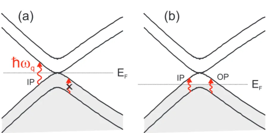
phonon mode when the Fermi level is at the K point. The frequency of the out-of-phase vibration is, then, higher then the frequency of the in-phase vibration forEF = 0.
If the Fermi energy is now moved away from the K point, the intraband electron-hole pairs can be produced by phonons (see Fig. 2.13). In this case, the OP phonons also have their energies renormalized, giving rise to the Kohn anomaly. Figs. 2.14(a) and (b) show, respectively, the frequency shift (solid lines) and the line width broadening (dashed lines) of the IP and OP phonon modes as a function of the Fermi energy calculated by T. Ando [33]. The δ parameter is due to disorder in the crystal. The frequency of the IP mode undergoes a hardening with increasing EF and exhibit a logarithmic singularity at EF =~ω/2, while a narrowing of the line width is observed. The renormalization for this
phonon mode is analogous to the case of monolayer graphene. For the OP phonons, with the increase of EF, the intraband transitions contributes now to the phonon self-energy, and the frequency of this mode gradually decreases, and a small broadening of the line width can be observed.
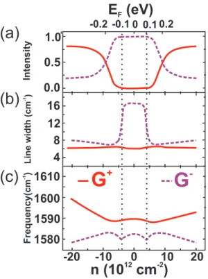
symme-Figure 2.15: Inversion symmetry-breaking induced phonon mixing. Evolution of the G+
(full lines) and G− (dashed lines) (a) relative intensity, (b) line width and (c) frequency
with carrier concentration and Fermi energy. The vertical dotted lines indicate a special position of the Fermi level, 0.1 eV, that corresponds to half of the G-band energy. Figure adapted from Ref. [36].
try of bilayer graphene is broken, lowering the symmetry of the system, that now belongs to the C3v point group [34], and opening an electronic band gap at the K point. As a consequence, the in-phase and the out-of-phase lattice vibrations are no longer eigenstates os the system, but the resulting eigenstates can be regarded as superpositions of the IP and OP displacements [35,36]. Since the Raman active mode (in-phase) is now present in both resulting modes, there will be two peaks in the Raman spectrum: one with lower frequency G− and another with higher frequency G+.
The Raman spectrum can be quantitatively analyzed using a simple coupled-mode description [36]
E−EIP g g E−EOP
= 0, (2.61)
between the IP-OP modes. Solutions to Eq. 2.61 are given by
E±= EIP +EOP
2 ±
√ (
EIP −EOP 2
)2
+g2, (2.62)
so that the real and imaginary parts ofE±, respectively, describe the energy and
broaden-ing of the G+ and G− modes. The behavior of the relative intensities, the width
broaden-ing and the frequency shift of the G+ and G−peaks as a function of the charge concentra-tion and Fermi energy is shown in Figs. 2.15(a), (b) and (c), respectively [36]. The peak intensity is determined by the size of EIP content within each mode. AtEF =±200 meV, the two peaks in the Raman spectrum have the same intensity as shown in Fig. 2.15(a) because the coupling partitions of the Raman active Eg mode is equally distributed to the G+ and G− peaks. Away from EF = ±200 meV, the relative intensities of the G+
and G− reverse, reflecting the fact that G− (G+) is dominated by the IP vibration at low
(high) charge concentration.
Chapter 3
The Raman spectroscopy of
graphene
The Raman spectrum of graphitic materials is known to be very sensitive to struc-tural changes, making the Raman spectroscopy to be widely used in the past four decades for the characterization of these systems. Moreover, the physics behind the Raman spec-trum of graphene is rich and can give us information about the electronic and vibrational structure, as well as the interactions about the electrons and phonons in the material. This chapter will start with a summary of the history of the Raman spectroscopy, fol-lowed by an overview of the first order and the double-resonance model, which successfully explains many features in the Raman spectra of monolayer and bilayer graphene.
3.1
Introduction of Raman Scattering
Light scattering is one of the most powerful tools for studying fundamental physics and material properties in condensed matter sciences. In the case the scattered light has the same frequency (wavelength) as the incident light, the process is elastic, and is known as Rayleigh scattering. If, however, after scattering, the light has a different frequency, the photon is then inelastically scattered, and a quantized excitation has been created or annihilated in the material and, in this case, the light scattering process is known as the Raman effect. It was discovered in 1928 by the Indian physicist Chandrasekhara Venkata Raman for which he was awarded the Nobel Prize in Physics in 1930. Nowadays, Raman spectroscopy is a widely used tool for characterization of liquids, gases, and solids, as well as for studying fundamental physics.
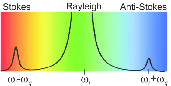
Figure 3.1: Schematics of the Raman spectrum where an incident light with frequency
ωi generates an elastically scattered light (Rayleigh) and two inelastically scattered com-ponents with frequency ωi−ωq (Stokes) andωi+ωq (anti- Stokes).
properties. The incident laser light ωi interacts with the material and creates a quantum excitationωq in the material system, the scattered lightωsthen has a different energy and line width from the incident photon. When the incident or scattered light coincides with the electronic gap of the material, we call this a resonant process. The energy difference between the incidentωi and scattered photon is determined by the energy of the quantum excitation, which is a measurement of the intrinsic property of the material:
ωs=ωi−ωq. (3.1)
This process is termed as the Stokes Raman scattering, where a phonon is created in the material, as illustrated in Fig. 3.1. Another possibility is that the laser light annihilates a phonon that was already in the material before the scattered light is emitted. In this case,
ωs=ωi+ωq, (3.2)
and the process is known as the anti-Stokes Raman scattering. In this thesis, we will only consider the Stokes Raman scattering.
Two conservation laws must be obeyed during the Raman scattering. The first one is energy conservation which was just discussed above. The second one is momentum conservation. The selection rules associated with the momentum conservation in the anti-Stokes and Stokes one-phonon Raman are given by:
Figure 3.2: (a) First order Raman process that gives rise to the G band. Second order double resonance Raman processes involving (b) intravalley and (c) intervalley phonons.
where the ±signal stands for the anti-stokes and for the stoke scattering, respectively. In fact, these relations strongly restrict the wavevectors of phonons involved in the scattering process, as we will show below.
3.2
First order Raman scattering
The light we use in Raman scattering is typically visible or near infrared. It has a wavelength of thousands of ˚A, which is 3 orders of magnitude larger than the unit cell size of graphene. The momentum of light is then negligible compared with the size of the Brillouin zone. Conservation of momentum then requires that the phonons have practically zero momentum. For first-order Raman scattering, this means that the only mode allowed would be the zone-center optical phonon. In a second-order Raman process, that will be explored in the next section, the phonons allowed include overtones and combinations, which are excitations with two phonons coming from the same or different phonon branch and having opposite momentum. The momentum of individual phonons may take any value.
The first order resonant Raman process can be understood as follows: a photon is absorbed by the material and excites an electron from the valence to the conduction band. The electron is then scattered by a phonon and then, recombines with the hole emitting a scattered photon. A schematics of this process can be seen in Fig. 3.2(a) for the stokes process, where the electron loses energy to create a phonon.
We now come to the phonon spectrum of graphene. Fig. 3.3 show the most promi-nent features in the Raman spectra of defect free monolayer graphene, the so called G band, appearing at ∼ 1582 cm−1, the G⋆ and the G′ bands at about 2450 cm−1 and
2700 cm−1, respectively. In the case of a disordered or defective sample, we can also see
the so-called D band, at about half of the frequency of the G′ band (around 1350 cm−1).
Figure 3.3: Typical Raman spectrum of defect free monolayer (upper) and bilayer (lower) graphene, showing the main Raman features G, G⋆ and G′ bands.
zone-center phonon mode. The G band is the only first order feature Raman active in graphene systems. As seen in Section 2.3, the E2g zone-center phonon mode is composed by the LO and iTO phonon branches. In bilayer graphene, there are now two valence and two conduction bands. Also, the E2g mode splits into Eg and Eu mode. However, only the Eg mode is Raman active and the G band of bilayer graphene is still composed of one peak.
3.3
Second order Raman scattering and the double
resonance process
The G⋆ and the G′ bands originate from a second-order Raman process. The G⋆ peaks is asymmetric and is composed of two peaks, one involving two iTO phonons with q∼0 (measured from the K point) and the other involving one LA and one iTO phonons with q ≈2k (also measured from the K point). The G′ band involves two iTO phonons
with q∼0 (processes (1) and (2)) and q ∼2k (processes (3) and (4)).
Both the iTO+LA from the G⋆ and the G′ peaks exhibit a dispersive behavior,i.e.,
their frequencies in the Raman spectra change as a function of the laser excitation energy EL. The G′ frequency ωG
′ upshifts with increasing EL in a linear way over the visible
range, with slope (∂ωG′/∂EL) around 100 cm−1/eV [17]. On the other hand, the iTO+LA
mode of the G⋆ band downshift with increasing the laser excitation energy, and its slope (∂ωG⋆/∂EL) is about−16 cm−1/eV [37].
The dispersive behavior of the frequency of the q ≈ 2k bands originates from a double resonance Raman (DRR) process [38–40]. The double resonance process, shown in Figs. 3.2(b) and (c), begins with an electron of wavevector k, measured from the K
point, absorbing a photon of energy EL. The electron is inelastically scattered by a phonon of wavevectorq and energyEph to a point around the K′ point, with momentum
k′ measured from K′. The electron is then scattered back to the k state, and emits a
photon by recombining with a hole. The DRR mechanism can be an intervalley process, when it connects states around inequivalent K and K′ points in the first Brillouin zone of
graphene, as shown in Fig. 3.2(c), and this is the case for both G⋆and the G′bands. There
is also the possibility of an intravalley process, where the scattering of the electron by the phonon connects two points belonging to the same K point, as shown in Fig. 3.2(b) [39].
When EL is increased, the resonance for the k vector of the electron moves away from theKpoint. In the DRR process, the correspondingqvector for the phonon increases with increasingk. Thus by changing the laser energy, we can probe the phonon dispersion relation (ω versus q). This effect is obtained experimentally from the dispersion of the phonon energy as a function of EL [17]. A tunable laser system can directly show this dispersive behavior for the G⋆ and the G′ bands in the Raman spectrum.
Since the monolayer graphene has only one conduction and one valence band, there is just one possible scattering process to give rise to the G′ band (the process shown in
Fig. 3.2(c)), and then, the G′ band of the monolayer graphene is composed of only one
peak.
In the case of AB stacked bilayer graphene, there are two valence and two conduction bands and the phonon branches split also affected by the interlayer interaction. Then, in the case of bilayer graphene, the DRR conditions involve more combinations than in the case of monolayer graphene, where there is only one main contribution to the G′ band.
Figure 3.5: Schematic view of the electron dispersion of bilayer graphene near theK and
K′ points showing π
1 and π2 valence bands and π1⋆ and π2⋆ conduction bands. The four
DRR processes are indicated: (a) process P11, (b) process P22, (c) process P12, and (d)
process P21. The phonon symmetries are also indicated in each process. (e) Measured G′
Raman band of bilayer graphene for 2.41 eV laser energy and fitted with four Lorentzians, each one corresponding to one of the possible process.
the T axis (ΓK) along which the π2 and π1⋆ bands belong to the T1 totally symmetric
irreducible representation, while theπ1andπ2⋆bands have odd T2symmetry relative to the
inversion symmetry [28]. Now, for computing the number of resonant conditions involved in the DRR process, we are left with electrons in only two excited electronic states withk vectors near the K point which will be scattered by a phonon to an electronic state with wavevectors near the K′ point. This electron-phonon scattering can now occur involving
phonon with two symmetries T1 and T2. For the case of a T1 phonon and the electron
can be scattered to bands with the same symmetry, i.e., π⋆
1 →π1⋆ and π⋆2 → π⋆2. On the
other hand, the T2 phonon will connect electronic bands with different symmetry, i.e.,
π⋆
1 →π⋆2 and π2⋆ →π⋆1 [28].
These four different Pij processes are depicted in Figs. 3.5(a)-(d), wherei(j) denote the electron scattered from (to) each conduction band π⋆
i(j). Processes P11 and P22 come
from an iTO phonon with T1 symmetry, while processes P12 and P21 come from an iTO
phonon with T2 symmetry. These four different scattering processes give rise to four
Raman peaks in the G′ spectrum. Fig. 3.5(e) shows the Raman spectra of a bilayer
graphene sample fitted with four Lorentzians with a decay line width of ∼ 25 cm−1 for
each peak.
and fast technique to identify the number of layers in a sample, since the shape of the G′ band depends on the number of layers of the sample [41]. It is important to notice
that the identification of the number of layers by Raman spectroscopy is well established only for graphene samples with AB Bernal stacking. Graphene samples made by the mechanical exfoliation of natural or HOPG graphite leads to graphene flakes that have predominantly AB stacking, but this is not necessarily the case for graphene samples made by other growth methods [16].
3.4
Raman instrumentation
Two different comercial triple-monochromator spectrometers were used in this the-sis: a Dilor XY system and a Horiba Jobin-Ivon T64000 system, both of them equipped with a N2 cooled Charge Coupled Device (CCD) detector (the CCD needs a temperature
of -140oC to properly work), working in the backscattering configuration. The CCD can be understood as a large area of silicon photodiodes that form a bi-dimensional array of pixels. Through the photoelectric effect, the photodiodes convert photons into photoelec-trons that are electronically processed. Each pixel delivers information compatible with the numbers of counts in it.
Figure 3.6: (a) In a monochromator scheme a grating (Gr) is geometrically connected to two spherical mirrors (SM1 and SM2) and two planar mirrors (PM1 and PM2). (b) The triple-monochromator is composed of a foremonochromator and a spectrograph. The foremonochromator is composed of two gratings that work harmonically in a configuration that basically filter the Rayleigh component and select a specific spectral range. The other grating composes the spectrograph where the beam is dispersed and reach a set of CCD’s pixels.
the beam is dispersed by the grating Gr3. This dispersion covers a complete set of the CCDs pixels. In a triple-monochromator, the three gratings can be rotated simultane-ously by a sine arm in order to chose the range of frequencies that will be covered by the CCD’s pixels. Also, it is possible to measure Raman bands much closer to the Rayleigh light when compared to the single-monochromator mode. However the biggest problem of triple-monocromator is that the light intensity is reduced by a factor of 5-10 when compared to the monochromator due to the additional gratings.
Chapter 4
Graphene and device fabrication
In this chapter we discuss the experimental methods which were used in this work. Here, we describe the equipments and techniques used to prepare graphene samples and to fabricate these raw materials into the field-effect transistors studied in subsequent chapters.
4.1
Sample preparation
There are several known methods of producing graphene. The first method em-ployed, and the one still widely used by the research community, is mechanical exfoli-ation [42]. The most recently developed method, and perhaps the most promising in prospects of scalability, is chemical vapor deposition [7,43,44], where the heat is used to break apart gas phase molecules and to reassemble these molecular components into a solid form. Usually, a catalyst film is used to enhance the breakdown of carbon gases beyond that possible with heat alone, and to act as a template for the self-assembly of carbon atoms into graphene.
Another possible graphene fabrication method is the annealing of SiC [45]. When a crystal of this material is annealed under the right conditions, the Si atoms will evaporate leaving behind a carbon-rich surface. The carbon atoms will self-assemble into graphene sheets, guided by lattice matching with the SiC surface. Also, there is the graphene oxide method [46], in which a chemical treatment is used to oxidize the graphite. The layers are then dispersed in water, and are carried off in dispersion. This solution may be filtered or cast onto a substrate to recover the graphene oxide material. Treatment with reducing chemical agents recovers much of the graphene to its original form.
(a)
(b)
(d)
(c)
Figure 4.1: Mechanical cleavage of graphite into graphene using a scotch tape. After successively exfoliation, the graphene is then deposited on a silicon substrate.
graphene sheet (the quality is determined primarily by the starting material). Since we are interested in the basic properties of graphene, this is the method of fabrication used in this thesis, and will be discussed in detail below.
4.1.1
Mechanical exfoliation
The mechanical exfoliation of graphite is possible due to the weak van der Waals interlayer coupling in layered materials like graphite [5]. By using a scotch tape it is possible to separate the graphite layers until you reach only one layer of graphene. This technique is exemplified in Fig. 4.1, where a thick piece of natural graphite is successively cleaved using a scotch tape and then deposited on a silicon/silicon dioxide substrate. Although being only one atom thick, contrast in the optical microscope is possible because the presence of the graphene changes the interference condition for light passing through the silicon dioxide and reflecting off the silicon [42,47]. The scotch tape used here was the Medium Tack Blue from the Semiconductor Equipment Corporation, USA, and the graphite was from the Nacional de Grafite Ltda., Brazil.
above with nitrogen. For a better cleaning, the substrate can be exposed to an oxygen plasma or to an UV-ozone camera (a small concentration of ozone gas generated by an ultraviolet lamp) for about 10 minutes. After the deposition, optical inspection in the optical microscope is performed over the substrate to localize the graphene flakes. The number of layers of the flake is confirmed by Raman spectroscopy as described in Section 3.3 [41].
4.1.2
Lithography
After the flakes identifications, the fabrication of electronic devices from graphene draws strongly from conventional silicon processing and microfabrication. The first part of the device fabrication consists of doing the lithography, in which a beam exposes a resist that has been coated onto the surface. Immersion of the resist in a developing solution causes the pattern to be revealed in a manner depending on the type of resist used. I have used two types of lithography for the device patterning in this work. During my period in Universidade Federal de Minas Gerais (UFMG), the optical lithography was used, while the e-beam lithography was used when I was at Massachusetts Institute of Technology (MIT). The two processes are described below as used in this work.
Optical Lithography
For the optical lithography, a photosensitive resist is deposited over the substrate and exposed by an ultraviolet light. The resist used here was the S1805 positive resist (areas exposed to the optical beam develop away and are removed). S1813 can also be used with the same parameters described here. The resist is spun in the substrate using two steps in the spin-coater: the first one with 1000 rpm spinning speed for 5 seconds, and the second one with 8000 rpm for 40 seconds. The samples are then baked at 115oC for 90 seconds. With these parameters, the thickness of the resulting deposited resist is
∼500 nm.