Abstract— We demonstrate the feasibility of using effective medium theory to reduce the computational complexity of full-wave models of inductors that are placed over interconnects. Placing inductors over interconnects is one way that designers can tackle the problem of reducing overall chip size, however this has heretofore been a difficult option to evaluate because of the prohibitive memory requirements and run times for detailed simulations of the inductor. Here we replace the interconnects with a homogeneous equivalent layer that mimics their impact on the inductor to within 2% error, but reducing runtime and memory use by 90% or more.
Index Terms—Effective medium theory, interconnects, spiral inductor.
I. INTRODUCTION
In contemporary integrated circuits the on-chip inductors occupy a significant area. This limits the
potential for down scaling the size of the chip, and has a concomitant cost implication. Since inductor
sizes do not scale with process geometry, the problem is exacerbated, leading researchers to consider
how the area underneath the inductor might be put to better use [1]. One option is to place
interconnects underneath, but this raises difficulties with the simulation of the inductor. Simulation of
the inductor is important because the three main parameters determining the performance of a spiral
inductor, namely inductance, quality factor and self-resonant frequency, are influenced by the
presence of nearby conductors. In contemporary CMOS technology dummy metal fill patterns are
used to ensure the adequate metal density. The effect of specific dummy patterns on the inductor
parameters where the metal fill is located on the same metal layer as the inductor, or underneath, has
already been reported [2]-[4]. The influence of patterned ground shields has also been studied [5]-[8].
However more of these cases relate to the particular geometry, alignment and location of interconnect
layers as would be found underneath an inductor. Specifically, interconnects are long narrow roads in
which significant induced currents can occur, unlike dummy fills or patterned ground shield, that are
designed to minimize such effects.
The particular difficulty in modeling an inductor located over an interconnect stack is large number
of features that require to be meshed (leading to excessive memory usage) and also the large ratio
between the wavelength (centimeters) and the sub-micron structure size that leads to numerical
Simplified Model of Interconnect Layers
under a Spiral Inductor
Sonia M. Holik, Timothy D. Drysdale,
Electronics Design Centre, Division of Electronics and Nanoscale Engineering, School of Engineering, University of Glasgow, Glasgow, G12 8LT, United Kingdom,
inefficiencies in time-domain techniques [9]. Nonetheless, isolated structures can be solved given
sufficient computational resource and time [10], or the analysis can be split into smaller
segments [11]. Here we propose an alternative approach that deliberately exploits the mismatch in
size between the wavelength and the structure, arising from earlier work in homogenizing
interconnects [12]- [14]. We intend to demonstrate the feasibility of the approach by example, leaving
a detailed development of a general method to future work.
II. SPIRAL INDUCTOR STRUCTURE
This section describes the structure of the exemplar spiral inductor studied in this paper as well as
giving an overview of the homogenization process.
A. Numerical Model
A proprietary full vector 3D frequency domain electromagnetic solver tool was used throughout
(HFSS) [15]. The exemplar conductor structure was designed to suit a conventional CMOS
interconnection technology [16], [17]. We consider up to three layers of dense interconnects beneath
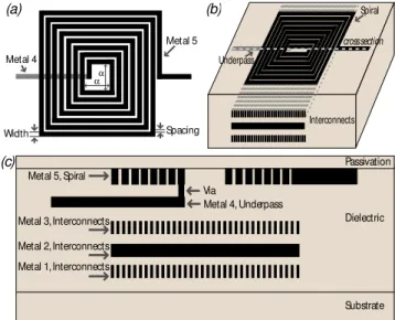
the inductor. The interconnects layers are mutually perpendicular as it is shown in Fig. 1, with the top
layout view of 7.5 turn rectangular spiral inductor of inner diameter α = 100 m, width 10 m and
spacing 2 m in Fig. 1a, a perspective view of the spiral inductor with metal rods aligned in parallel
on the mutually perpendicular metal layers underneath the inductor in Fig. 1b, and a cross section of
the structure in Fig. 1c.
Width Spacing
α
Metal 4
Metal 5
Metal 5, Spiral
Metal 4, Underpass Via
Metal 3,Interconnects
Substrate Passivation
Dielectric
cross section
Spiral
Underpass
Interconnects
α
(a) (b)
(c)
Metal 1,Interconnects Metal 2,Interconnects
Fig. 1. The geometry of the spiral inductor: (a) top layout view of the rectangular spiral; (b) perspective view with metal rods underneath the spiral; (c) cross section of the structure.
The inductor is defined in the top most metal, Metal 5, a 1.1 m thick layer of low conductivity
aluminum σ = 30x106 S/m. The underpass at Metal 4 has thickness 0.75 m. The isolating
silicon-oxide layer between Metal 4 and Metal 5 is 0.8 m thick, while between Metal 3 and Metal 4, Metal 2
and Metal 3, Metal 1 and Metal 2, as well as Metal 1 and the substrate, it is 1 m thick. The 1.1 m
metal (copper) rods not connected to the ground. The rods (330 elements on each metal layer) are
aligned in parallel, and have length of 300 m in order to cover the entire span of the inductor. The
rods have width 0.45 m and height 0.9 m giving an aspect ratio of 2. The space between the rods is
0.45 m, giving a metal fill factor of 0.5. The rods and inductor were modeled using layered
impedance boundary conditions. The substrate is defined as 15 -cm resistivity silicon of thickness
625 m and is grounded by the perfect electric boundary conditions defined at the bottom plane, while
other walls were defined as radiation boundaries. The spiral was covered by a 60 m thick
silicon-nitrate passivation layer.
B. Homogenization Approach
In order to homogenize the interconnect structure we use a modified Maxwell-Garnett (MG) mixing
rule [12], [13] to calculate the effective permittivity of the homogeneous equivalent layer
εeff =εe+ Ψfεe εi−εe
εi+2εe−f
(
εi−εe)
(1)where εi and εe are the dielectric functions of the inclusion and host material respectively (here, a
metal and a dielectric), Ψ is a constant relating the fields inside and outside the inclusions (typically
Ψ = 3 for spherical inclusions), f is the filling factor or ratio of the volume of the inclusion to the total
size of the unit cell. The Maxwell-Garnett rule is known to give a qualitatively correct prediction of
the effective properties of a composite with conducting inclusions [18]. The frequency dependant
dielectric function of a metal inclusion εi is expressed by a Drude model [19].
III. NUMERICAL RESULTS
This section presents the obtained numerical results. First it shows the dependence of the
performance of the inductor on the number of interconnect layers under the spiral. Further, the
homogenization approach is numerically validated.
A. Interconnect Layers Dependence
It is well known that metal structures in the vicinity of inductors have an influence on their
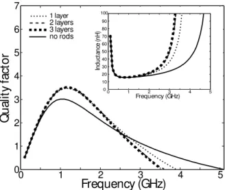
performance. Here we examine and demonstrate in Fig. 2 the relationship between the number of
0 1 2 3 4 5 0
1 2 3 4 5 6 7
Frequency (GHz)
Q
u
al
it
y
fa
ct
o
r
1 layer 2 layers 3 layers no rods
0 1 2 3 4 5
0 10 20 30 40 50 60 70 80 90 100
Frequency (GHz)
In
d
u
ct
an
ce
(n
H
)
Fig. 2. The quality factor and inductance as a function of frequency for rectangular
spiral inductor with various numbers of metal layers placed underneath the spiral.
Only the two topmost layers consisting mutually perpendicular metal rods under the inductor
significantly changes the electromagnetic field and inductor’s electrical characteristic. The reference
structure defined as an inductor with no metal rods underneath has inductance of 16 nH, a maximum
Q-factor of 3.04 at 1.1 GHz, and self-resonant frequency (SRF) of 5.1 GHz. When the entire area on
Metal 3 was filled with metal rods the value and the frequency of the maximum Q-factor has change
to 3.5 at 1.2 GHz, and the SRF dropped by 23% to 3.9 GHz. Further when the mutually perpendicular
layer of metal rods was included on Metal 2 the maximum Q-factor remain the same but the SRF falls
to 3.5 GHz (31%). Simulations indicate that including the third metal layer on Metal 1 or extending
the interconnect stack by adding more metal layers (not shown here) does not significantly change the
characteristic parameters of the inductor. This is because the parasitic capacitance is primarily
determined by the two topmost metal layers. The inset plot of the inductance depicts that the SRF
reduces with the different number of metal layers added underneath the spiral.
B. Homogeneous Equivalent Structure
In order to reduce the complexity of the model we replaced the layers of metal rods with a
homogenous equivalent layer of the same thickness of 1.1 m as the rods. In the empirical fitting
procedure the linearly distributed values of the scaling factor Ψ were sampled within the interval of 1
to 10000 with the step increment of 100. For the particular geometry arrangement denser sampling of
the values of Ψ does not reflect in notable change in the characteristic inductor’s parameters. It was
found that for the spiral inductor with one layer of metal rods underneath the fitted value of complex
effective permittivity which gives good approximation of the characteristic parameters in the
considered frequency range 1-8 GHz can be calculated from Eq. 1 with coefficient Ψ = 900
(εeff = 3604 + 9.5232x10
-4
i). The results from the EMT simulation are compared against the detailed
increased error up to 10% above SRF. Better approximation has been obtained for the structure with
two layers of mutually perpendicular rods underneath the inductor. This indicates that an anisotropic
homogenous equivalent layer may be required for the special case where interconnects are aligned
along a single axis only.
0 1 2 3 4 5
0 1 2 3 4 5 6 7
Frequency (GHz)
Q
u
al
it
y
fa
ct
o
r
1 layer 2 layers 1 layer MG 2 layers MG no rods
0 1 2 3 4 5
0 10 20 30 40 50 60 70 80 90 100
Frequency (GHz)
In
d
u
ct
an
ce
(n
H
)
Fig. 3. The quality factor and inductance as a function of frequency for rectangular spiral inductor with one and two metal layers placed underneath the spiral. Results from homogenized equivalent structure are drawn as markers.
The empirically found value of εeff = 16004 + 4.2325x10
-3
i (Ψ = 4000) gives good agreement between
the detailed and homogenized structure with an error less than 2% over entire frequency range. The
value of Ψ and affiliated εeff is much higher than in the case of standalone structures [12], [13], and
this corresponds to the change of the character of the illumination away from a plane wave. Also, in
certain mixing ratios, mixtures with conductive constituents can have a larger value of the real part of
εeff than either of the components [17].
Applying the EMT techniques reflects in significant reduction in computational time (69% for one
layer and 95% for two layers under the inductor) and allocated memory (51% and 90% for one and
two layers underneath, respectively). Regarding to the fact that only the two topmost layers of metal
rods influence the change in inductor’s parameters even higher reduction in computational time and
allocated memory can be predicted for structures with additional interconnect layers. These promising
results justify the displacement of further effort in obtaining more general results for the value of εeff
for the range of structures designers are likely to account for.
IV. CONCLUSION
The numerical results presented in this paper show that multilayered interconnect structures with
mutually perpendicular layers of parallel metal rods that are located underneath a spiral inductor can
be replaced with a homogenous equivalent layer. The effective permittivity of this layer is calculated
using the effective medium theory via a modified Maxwell-Garnett mixing rule. Using the
with an error of less than 2%, whilst reducing the runtime and memory usage by 90% or more. We
expect that using a similar approach to our earlier work, empirical expressions can be developed to
give the required fitting parameter across the range of inductor and interconnect structures that
designers are likely to encounter, although we leave this significant effort to future work.
REFERENCES
[1] F. Zhang, and P. R. Kinget, “Design of components and circuits underneath integrated inductors,” IEEE J. Solid-State Circuits , vol. 41, no. 10, pp. 2265-2271, 2006.
[2] J. H. Chang, Y. S. Youn, H. K. Yu, and C. K. Kim, “Effects of dummy patterns and substrate on spiral inductors for
sub-micron RF ICs,” IEEE Radio Frequency Integrated Circuits Symposium, Digest of Technical Papers, pp. 419-422, 2002.
[3] C. L. Chen, “Effects of CMOS process fill patterns on spiral inductors,” Microwave and Optical Technology Letters,
vol. 36, no. 6, pp. 462-465, 2003.
[4] H. M. Hsu, and M. M. Hsieh, “On-chip inductor above dummy metal patterns,” Solid State Electronics, vol. 52, pp. 998-1001, 2008.
[5] K. Murata, T. Hosaka, and Y. Sugimato, “Effect of a ground shield of a silicon on-chip spiral inductor,” Proc. IEEE Microwave Conference, pp. 177-180, 2000.
[6] C. P. Yue, and S. S. Wong, “Design strategy of on-chip inductors for highly integrated RF systems,” Proc. IEEE Design Automation Conference, pp. 982-987, 1999.
[7] J. Chen, and J. J. Liou, “On-chip spiral inductors for RF applications: an overview,” J. Semiconductor Tech. Science, vol. 4, no. 3, pp. 149-167, 2004.
[8] X. Sun, G. Carchon, Y. Kita, K. Chiba, T. Tani, and W. De Raedt, “Experimental analysis of above-IC inductor performance with different patterned ground shield configurations and dummy metals”, Proc. 36th UMC’06, pp. 40-43, 2006.
[9] S. M. Holik, and T.D. Drysdale, ”Simplified model of a layer of interconnects under a spiral inductor”, accepted for publication in Journal of Electromagnetic Analysis and Applications.
[10]J. Choi, M. Swaminathan, B. Beker, and R. Master, “Modeling of realistic on-chip power grid using FDTD method,”
Proc. IEEE Int. Sym. Electromagnetic Compatibility, vol. 1, pp. 238-243, 2001.
[11]A. Fontanelli, “System-in-package technology: opportunities and challenges,” Proc. IEEE Int. Sym. Quality Electronic Design, pp. 589-593, 2008.
[12]S. M. Holik, and T. D. Drysdale, “Simplified model for on-chip interconnects in electromagnetic modeling of
system-in-package,” Proc. 12th ICEAA’10, pp. 541-544, 2010.
[13]S. M. Holik, and T. D. Drysdale, “Effective medium approximation for electromagnetic compatibility analysis of integrated circuits,” Proc.2nd ICAEMMO’08, pp. 413-415, 2008.
[14]S. M. Holik, T. D. Drysdale ’Simplified model of a layer of interconnects under a spiral inductor,’ J. Electromagnetic Analysis and Applications, vol. 3, no. 6, pp. 187-190, 2011.
[15]Ansoft High Frequency Structure Simulator (HFSS). http://ansoft.com/
[16]M. Park, S. Lee, C. S. Kim, H. K. Yu, and K. S. Nam, “The detailed analysis of high Q CIMOS-compatible microwave
spiral inductors in silicon technology,” IEEE Trans. Electron Devices, vol. 45, no. 9, pp. 1953-1959, 1998.
[17]M. Park, G. H. Kim, J. Jang, J. G. Koo, and K. S. Nam, “Planarised interconnection technology using a new pillar formation method with multistacked metal structure,” Electron. Lett., vol. 32, no. 18, pp. 1731-1732, 1996.
[18] A. Sihvola, , “Electromagnetic mixing formulas and applications,” IEE Publishing, London, 1999.