Thickness dependence of leakage current in BaBi 2 Ta 2 O 9 thin films
C. R. Foschini, E. Longo, J. A. Varela, and S. B. DesuCitation: Applied Physics Letters 75, 552 (1999); doi: 10.1063/1.124419 View online: http://dx.doi.org/10.1063/1.124419
View Table of Contents: http://scitation.aip.org/content/aip/journal/apl/75/4?ver=pdfcov Published by the AIP Publishing
Thickness dependence of leakage current in BaBi
2Ta
2O
9thin films
C. R. Foschini,a)E. Longo, and J. A. VarelaInstituto de Quı´mica, Universidade Estadual Paulista-UNESP, 14801-970 Araraquara, SP, Brazil S. B. Desu
Department of Electrical and Computer Engineering, University of Massachusetts, Amherst, Massachusetts 01003
~Received 4 January 1999; accepted for publication 23 May 1999!
BaBi2Ta2O9 thin films having a layered structure were fabricated by metalorganic solution
deposition technique. The films exhibited good structural, dielectric, and insulating properties. The room temperature resistivity was found to be in the range of 1012– 1014Vcm up to 4 V corresponding to a field of 200 kV/cm across the capacitor for films annealed in the temperature range of 500–700 °C. The current-voltage (I–V) characteristics as a function of thickness for films annealed at 700 °C for 1 h, indicated bulk limited conduction and the log(I) vsV1/2characteristics suggested a space-charge-limited conduction mechanism. The capacitance–voltage measurements on films in a metal–insulator–semiconductor configuration indicated good Si/BaBi2Ta2O9interface
characteristics and a SiO2 thickness of;5 nm was measured and calculated. © 1999 American Institute of Physics.@S0003-6951~99!00830-X#
In recent years, there has been considerable interest in the ferroelectric Aurivillius compounds, since such materials are widely used in technical devices. BaBi2Ta2O9~BBT!
be-longs to the layer-perovskite family with a Curie temperature of 110 °C and a dielectric constant of 400, measured in bulk ceramics by Subbarao.1BBT thin films is an attractive ma-terial for very large scale integrated devices such as dynamic random-access memories ~DRAMs! because of its high charge storage capacity, good insulating property, and low leakage current.2,3 The application of BBT thin films to DRAM capacitors would enable the realization of ultralarge scale integrated DRAMs cells with a simple stacked struc-ture.
An approach to replace the existing SiO2 based
dielec-trics is the use of high dielectric constantermaterials.4,5The
problem with high dielectric constant materials is that most of them cannot be directly deposited on silicon. Moreover, the integration requires development of high temperature stable barrier-electrode systems, because of the interaction between the components. Among the high dielectric constant materials are Ta2O5(er522) and ~Ba, Sr!TiO3(er5400).
However, both have leakage current problems and the later have titanium, which rapidly diffuses into silicon and forms titanium silicide. Apart from this there is a possibility that BBT could be directly deposited onto Si substrate.
This letter describes the preparation of BBT thin films by metalorganic solution deposition ~MOSD! technique and its electrical characterization in terms of leakage current. The MOSD process, like almost all chemical methods, is well known in the area of processing thin films because of easier composition control, better homogeneity, low processing temperature ~compatible with Si processing!, easier fabrica-tion of large area thin films, and low cost.6
Thin films of BaBi2Ta2O9 were fabricated using barium
acetate (BaOOCCH3)2, bismuth 2-ethylhexanoate
(Bi~C7H15COO!3), and tantalum ethoxide (Ta~OC2H5!5) as
precursors. Acetic acid, 2-ethylhexanoic acid and 2-methoxyethanol were selected as solvents. Bismuth 2-ethylhexanoate and barium acetate precursors were dis-solved in 2-ethylhexanoic acid and acetic acid, respectively, under room temperature conditions. These solutions were then added to the solution of tantalum ethoxide in 2-methoxyethanol. The precursors films were deposited onto platinum coated silicon and bare silicon substrates by spin coating operated at 6000 rpm for 40 s. After spinning, films were kept on a hot plate at 350 °C in air for 10 min. After each coating this step was repeated to ensure complete re-moval of volatile matter. The crystallinity of the films was examined by x-ray diffraction ~XRD! and the cross-section silicon interface by transmission electron microscopy. The thickness of the films was measured by variable angle spec-troscopy ellipsometry. The electrical properties reported in-clude dielectric, capacitance–voltage, and current–voltage (I–V). The electrical measurements were conducted on films in metal–insulator–metal ~MIM! or metal–insulator– semiconductor ~MIS! configurations using Pt as the top and bottom ~MIM! electrodes. The top electrodes, area53.131024cm2, were deposited on the surface of films
by sputtering through a shadow mask. The dielectric proper-ties were measured with a HP 4192A impedance analyzer at room temperature and the leakage I–V characteristics were measured by means of a Keithley 617 electrometer/source.
The pyrolyzed films~at 350 °C!were found to be amor-phous and postdeposition annealing was required to develop crystallinity. The structure of the films was analyzed by a Scintag XDS 2000 diffractometer using CuKa radiation at
40 kV. Figure 1 shows the XRD patterns of films annealed in the range of 450–700 °C for 60 min. A well-crystallized orthorhombic phase was attained at 700 °C. The XRD pat-terns also revealed that films were polycrystalline in nature with no evidence of preferred orientation or secondary phases. The significantly lower processing temperature of
a!Electronic mail: [email protected]
APPLIED PHYSICS LETTERS VOLUME 75, NUMBER 4 26 JULY 1999
552
0003-6951/99/75(4)/552/3/$15.00 © 1999 American Institute of Physics
BBT thin films compared to bulk sintering temperature shows the possibility of exploiting thin films for microelec-tronic devices. The films also exhibited a dense microstruc-ture and the grain size was very fine.
The characteristics of electrical conduction were mea-sured using MIM capacitors. The insulating properties of the films were found to be dependent on the temperature of an-nealing. As shown in Fig. 2, room temperature resistivity and leakage current density were greatly changed by the anneal-ing temperature. The room temperature resistivity was found to be in the range of 1012– 1014Vcm up to 4 V correspond-ing to a field of 200 kV/cm across the capacitor for films annealed in the temperature range of 500–700 °C. The leak-age current density decreased with increase in the annealing temperature. Such reduction in leakage current density with increasing annealing temperature may be attributed to im-proved crystallinity and oxidation, leading to near perfect stoichiometry and completeness of the phase formation. Typical leakage current densities were lower than 1029
A/cm2 at an applied electric field of 200 kV/cm for films annealed at 700 °C for 1 h.
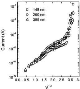
An understanding of the mechanism of nonlinear con-ductivity in thin film insulators is pertinent to the develop-ment of thin film devices for microelectronics. The steady state field dependent dc conductivity was examined through the measurement of theI–V characteristics in MIM capaci-tors. Several electrical processes allow electrical charges to move in insulators, leading to sizable current densities. The low field properties are usually ohmic in nature, that is, cur-rent Iis linear with voltageV. At high fields these behavior can be expressed by the empirical power lawI5KVa, where
K is a proportionality constant. Generally, the high field characteristics cannot be adequately described by a single conduction process; usually at different field strength ranges manifest different electrical phenomena. The thickness de-pendence of the I–V characteristics indicated bulk limited conduction.7–9These films exhibited high resistivities in the range of 1012– 1014Vcm at an applied electric field of 200 kV/cm, for 150–400 nm thick films. In this range of resis-tivities, the possible dominant conduction mechanisms may be:~a!tunneling,~b!Poole–Frenkel effect, and/or~c! space-charge-limited conduction. As the thickness of the films was above 100 nm, the tunneling process was ruled out. If the non-ohmic conduction is due to Poole–Freenkel flow, then we should get a straight line in log(I) againstV1/2
plot, which was not found in our case, as can be seen from Fig. 3. So the dominant bulk limited conduction mechanism was expected to be space-charge-limited-current~SCLC!conduction.
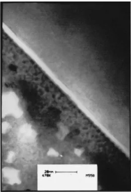
From the compatibility point of view, it is important to study the Si/thin film interface. The thickness of the SiO2
layer was calculated from the capacitance measurements on BBT thin films with 10% excess bismuth annealed at 700 °C/1 h using the MIS configuration, as schematized in Fig. 4. Platinum top electrodes, deposited by sputtering, of 3.131024
cm2 were used to form this structure. The total
FIG. 1. X-ray diffraction patterns of BBT thin films annealed at different temperatures for 60 min.
FIG. 2. Room temperature resistivity and leakage current density of BaBi2Ta2O9films as a function of annealing temperature, measured at an
applied electric field of 200 kV/cm.
FIG. 3. Log(I) vsV1/2. The nonlinearity indicates the absence of the Poole–
Frenkel effect.
FIG. 4. Schematic MIS structure used to calculate the SiO2thickness layer.
553
Appl. Phys. Lett., Vol. 75, No. 4, 26 July 1999 Foschiniet al.
capacitance measured in this configuration at 100 kHz was 140 pF.
The total capacitance CTot is modeled as consisting of
two capacitances in series, i.e., those of the BBT layerCBBT,
and those of the SiO2 layer CSiO2. Therefore, the total
ca-pacitance is given by
1
CTot
5 1
CSiO2
1 1
CBBT
, ~1!
where each capacitance is given by
C5e0erA
d , ~2!
whereer andd are the dielectric constant and the thickness
of the SiO2 layer or the BBT layer,e0 is the permittivity of
free space, and A is the area of the electrode spot being
tested. Assuming the values of er,SiO253.9; 5 e
r,BBT5283; 3
dBBT5187 nm measured by ellipsometry for this particular
specimen, and rearranging Eq. ~2!
dSiO25
e0eSiO2A
CSiO 2
55.06 nm. ~3!
The thickness of the SiO2layer in this specimen was also
measured from cross-sectional transmission electron micros-copy. As can be seen in Fig. 5, the measured thickness for the SiO2 layer is about 5 nm and agrees very well with the
calculated value from the capacitance data.
In conclusion, BaBi2Ta2O9 thin films with crystalline
structure were successfully prepared by the metalorganic so-lution deposition technique on Pt-coated Si and n1Si
sub-strates. Very well-crystallized BBT thin films were obtained after annealing at 700 °C for 60 min. The room temperature resistivity was found to be in the range of 1012– 1014Vcm
up to 4 V corresponding to a field of 200 kV/cm across the capacitor for films annealed in the temperature range of 500– 700 °C. Typical leakage current densities were lower than 1029
A/cm2 at an applied electric field of 200 kV/cm for films annealed at 700 °C for 1 h. The thickness dependence of theI–V characteristics indicated bulk limited conduction mechanism and the dominant conduction mechanism was ex-pected to be SCLC conduction. The SiO2thickness layer;5
nm indicated good Si/BBT interface characteristics.
The authors are grateful for the support of the FAPESP, CNPq, CAPES, and FINEP/PRONEX agencies from Brazil.
1E. C. Subbarao, J. Phys. Chem. Solids23, 665~1962!. 2
C. A-Paz de Araujo, J. D. Cuchiaro, L. D. McMillan, M. C. Scott, and J. F. Scott, Nature~London!374, 627~1995!.
3C. R. Foschini, P. C. Joshi, J. A. Varela, and S. B. Desu, J. Mater. Res.14,
1860~1999!. 4
P. C. Fazan, H. C. Chan, and V. K. Mathews, Semicond. Int. May, 108 ~1992!.
5M. Anthony, S. Summerfelt, and C. Teng, T. I. Tech. J., Sep–Oct, 30 ~1995!.
6L. C. Klein,Sol-Gel Technology for Thin Film, Fibers, Performs,
Elec-tronics and Specialty Shapes~Noyes, Park Ridge, NJ, 1988!.
7M. Stuart, Phys. Status Solidi23, 595~1967!.
8M. Roth and A. Burger, Appl. Phys. Lett.52, 1234~1988!. 9A. E. Rakhshani, J. Appl. Phys.69, 2365~1991!. FIG. 5. Cross-sectional transmission electron microscope micrograph
show-ing a 5 nm SiO2thickness layer.
554 Appl. Phys. Lett., Vol. 75, No. 4, 26 July 1999 Foschiniet al.