i UNIVERSIDADE FEDERAL DE MINAS GERAIS
INSTITUTO DE CIÊNCIAS EXATAS
DÉBORAH REIS ALVARENGA
A Study on the Physical Properties of
Quantum Dot Structures for Infrared
Photodetection
ii DÉBORAH REIS ALVARENGA
A Study on the Physical Properties of
Quantum Dot Structures for Infrared
Photodetection
Tese apresentada ao Instituto de Ciências Exatas da Universidade Federal de Minas Gerais para obtenção do título de Doutor em Física.
Área de concentração: Física do Estado Sólido Orientador: Paulo Sérgio Soares Guimarães Co+orientadora: Patrícia Lustoza Souza
iv
AGRADECIMENTOS
Em primeiríssimo lugar agradeço à minha família. Sem o apoio e o amor de vocês essa tese nunca existiria.
Ao meu orientador Paulo Sérgio, não apenas pela orientação dessa tese, mas pela amizade e carinho.
Aos professores Patrícia L. Souza, Wagner Nunes Rodrigues e Maurício Pamplona Pires pela co+orientação.
Ao Professor Karl Unterrainer e a todo o grupo da Universidade Técnica de Viena, especialmente ao Thomas Gebhard, à Barbara Weber e ao Alex.
Ao Carlos Parra e ao Zé Maria pelo trabalho teórico e pela amizade.
Aos professores e colegas do departamento de Física da UFMG, especialmente aos do grupo de Semicondutores.
Aos colegas e amigos da PUC+RJ e a todos os professores e alunos do DISSE. À Marluce, Ieda, Shirley e todos os funcionários que colaboram para o bom funcionamento do departamento.
À Rachel pela amizade, apoio e carinho durante todas as fases do doutorado. A todas as minhas amigas, amigos e familiares.
Foram 4 anos de dedicação. Ao longo desses anos várias pessoas contribuíram de alguma forma para a realização deste trabalho. Algumas, por motivos variados, não são mais presentes (ou são menos presentes) em minha vida. Agradeço a todos que contribuíram direta ou indiretamente para a realização desta Tese.
Ao CNPq, à CAPES, ao DISSE/INCT, ao Wolfgang Pauli Institute, pelo apoio financeiro.
v
RESUMO
Esta tese faz parte de uma proposta mais ampla cujo objetivo global é dominar a tecnologia de fotodetectores de radiação infravermelha baseados em pontos quânticos
semicondutores auto+organizados, os (QDIPs),
para a faixa de comprimento de onda de 2 a 20 m. A tese está centrada no estudo das propriedades físicas de pontos quânticos e de estruturas de QDIPs, em especial os mecanismos de transição intrabanda e de extração de carga envolvidos no processo de geração da fotocorrente. Foram estudadas estruturas inovadoras e originais baseadas em pontos quânticos auto organizados de InAs crescidos sobre substratos de InP. Para obter os principais resultados apresentados nesta tese foram feitas medidas de fotocorrente em função da temperatura e tensão externa aplicada, utilizando um espectrômetro de transformada de Fourier. As técnicas experimentais de fotoluminescência, microscopia de forca atômica, microscopia eletrônica de transmissão e curvas de corrente ! voltagem também foram utilizadas para obter uma melhor compreensão dos mecanismos físicos envolvidos. Para explicar os resultados e atribuir cada pico de fotocorrente a uma transição específica utilizamos um modelo teórico tridimensional. Os resultados que se destacam e são apresentados nessa tese são:
i. O efeito Auger intrabanda é apontado como um possível processo importante para gerar a corrente nos QDIPs. Medidas de fotocorrente intrabanda e de absorção, juntamente com um cálculo teórico tri+ dimensional, mostram que a transição responsável por gerar a fotocorrente medida em uma estrutura QDIP específica estudada ocorre entre estados ligados do ponto quântico onde o estado final da transição está 200 meV abaixo do contínuo. O espalhamento Auger é proposto como o mecanismo responsável pela extração de carga do ponto quântico, e portanto pela fotocorrente gerada, nesses dispositivos. Resultados de fotoluminescência e fotocorrente interbanda fornecem apoio adicional para esta conclusão.
vi dependem da estrutura como um todo. Os dispositivos aqui estudados apresentam fotocorrente com sentido positivo e negativo para a mesma tensão externa aplicada. Este duplo comportamento é atribuído à assimetria presente nessas estruturas, capaz de favorecer a extração de elétrons em um dos dois sentidos possíveis para a corrente. Esse processo foi observado apenas para pequenos valores de tensão externa aplicada. Para valores altos de tensão, os elétrons se propagam no mesmo sentido do campo elétrico aplicado, assim como esperado.
vii
ABSTRACT
This thesis is part of a project where the overall goal is to master the technology of infrared photodetectors based on self+organized semiconductor quantum dots, the Quantum Dot Infrared Photodetectors (QDIPs) for the wavelength range from 2 to 20 m. The thesis focuses on the physical properties of quantum dots and QDIPs structures, especially on the intraband transitions and extraction mechanisms involved in the photocurrent generation. We studied original and innovative structures based on self+organized InAs quantum dots grown on InP substrates. The main results presented in this thesis are based on photocurrent measurements as a function of temperature and external applied bias voltages, using a Fourier Transform Infrared spectrometer. The experimental techniques of photoluminescence, atomic force microscopy, transmission electron microscopy and current+voltage curves were also performed to achieve a better understanding of the physical mechanisms involved. To explain the results and assign each photocurrent peak to a particular transition, fully three dimensional theoretical calculations were done. The main results presented in this thesis are:
i+ It is shown that the intraband Auger effect can be an important process for the photocurrent generation in QDIPs. Intraband photocurrent and absorption measurements, together with a full three+dimensional theoretical modeling revealed that a bound+to+bound optical transition, where the final state is about 200 meV deep below the conduction band continuum, is responsible for the photogenerated current in the particular QDIP structure investigated. Photoluminescence and interband photocurrent spectra further support this conclusion.
viii one of the two possible senses of the current. This process is seen for small external applied bias voltages or when no bias is applied. For high external fields the photoexcited electrons go in the same sense of the applied field, as expected.
ix
CONTENTS
RESUMO... v
ABSTRACT ... vii
1. INTRODUCTION ... 1
2. QUANTUM DOT STRUCTURES ... 4
2.1 Introduction to Quantum Dot Structures. ... 4
2.2 Quantum Dot Formation ... 5
2.3 Techniques for Material Deposition ... 7
2.3.1 Molecular Beam Epitaxy ... 7
2.3.2 Metal+Organic Vapour Phase Epitaxy ... 8
2.4 Experimental Studies on Quantum Dots Grown by MOCVD ... 9
References: ... 12
3. INFRARED DETECTORS ... 13
3.1 Infrared Technology ... 13
3.2 Infrared Photon Detectors ... 15
3.2.1 Figure of Merit ... 15
3.2.2 Types of Infrared Photon Detectors ... 18
3.3 Stand out works on Quantum Dots Infrared Photodetectors ... 21
3.4 How to Produce a QDIP ... 23
References ... 26
4. THEORETICAL MODELING ... 28
4.1 Introduction ... 28
4.2 Description of the Method ... 28
References ... 34
5. EXPERIMENTAL TECHINIQUES ... 35
x
5.1.1 Sample Processing for Photocurrent Measurements ... 37
5.1.2 Sample Processing for Absorption Measurements ... 39
5.2 Current+Voltage Measurements ... 40
References: ... 42
6. RESULTS ... 43
6.1 Introduction ... 43
6.2 Evidences of Intraband Auger Process in Quantum Dot Infrared Photodetectors ... 44
6.3 Very Narrow Band QDIP Operating at 12 µm ... 54
6.4 Dual Sign Photocurrent in Quantum Dot Structures for Infrared Photodetection ... 59
References ... 67
1 1. INTRODUCTION
O. INTRODUCTION
The current technology of infrared (IR) detection is no longer fully attending the market needs. The rise of Information Technology and the Digital Economy require IR detectors with high sensitivity, high selectivity, high detectivity and low cost, small size and light weight. All of these requirements lead us to the development of new semiconductor technologies and materials.
With the advances in epitaxial growth of heterostructures a new class of material with unique optoelectronic properties has been developed. This new concept consists on zero dimensional quantum confined semiconductors heterostructures, called Quantum Dots (QDs), with several promising applications like more selective detectors, lasers, solar cells, and others. Researchers have studied the application of QDs in solar cells, LEDs (light emitting diodes), optical communication in free space, etc, apart from the wide application in imaging (including medical image). QDs have also been suggested as implementation of quibts for quantum information.
Much attention has been devoted to these heterostructures for mid+infrared photodetection applications. The interest on this zero dimensional structures is due to their potential for the development of selective infrared detectors operating close to, or even, at room temperatures, with high detectivity.
2 1. INTRODUCTION
radiation is intraband. It occurs in the conduction band (or in the valence band) between a bound quantum well state and a state in the continuum (or close to the continuum). This makes QWIPs more selective devices when compared to MCTs detectors. The main drawback of QWIPs is the presence of selection rules which forbid the absorption of normal incident light. The result is that QWIPs are not very efficient and they demand the use of diffraction gratings on top of the device or some other artifact to change the direction of normal incident radiation. Besides that, QWIPs only work at low temperatures due to a high dark current generated by the large density of states in quantum well structures when compared to quantum dot structures. In QDIPs the transitions involved in the detection are also intraband. As the QD confine the electron in all three dimensions the selection rules are no longer a problem in these structures. Also, since the energy levels are discrete, and not subbands as in QWIPs, the QDIPs are even more selective. Besides that, the longer life time of the carriers in these structures increases the detectivity.
The biggest problems faced by QDIPs nowadays are related to the difficult in controlling the QD size, density and homogeneity. These QD parameters are directly related to IR detector properties. For example, the QD size is one of the parameters that set the detection wavelength and the QD density and uniformity influence the detectivity.
In this thesis we present a study on new structures and materials for IR photodetection. We designed structures based on self+assembled InAs QDs grown by Metalorganic Chemical Vapor Deposition (MOCVD) on InP substrates. Nowadays there are only a few studies on the InAs/InP system for QDIPs. The most studied material system for the development of QDIPs is InAs/GaAs quantum dots. Although being formed by the same quantum dot material, the two systems differ in important points, which generate differences in the optical and electronic properties of the device. The most important difference is related to the lattice mismatch that is smaller for InAs/InP systems.
3 1. INTRODUCTION
structures, especially on the carrier extraction mechanisms. We show the importance of intraband Auger processes to generate a photocurrent. We study the influence of the final state of the transition on the carrier extraction mechanisms. We present a very selective QDIP structure which operates at around 12 µm. The final chapter is devoted to the main conclusions.
4 2. QUANTUM DOT STRUCTURES
2. QUANTUM
D
OT STRUCTURES
2.O Introduction to Quantum Dot Structures.
When we talk about Quantum Dots (QDs) we are talking about quantum confinement, which affects crucially the properties of particles and systems. A QD is the ultimate limit of confinement for carriers, since the particles are constrained in all 3 directions. This means that the electrons (and/or holes or excitons) are localized in space. As a consequence, the energy states allowed for the carriers are discrete, as in atoms [2.1].
5 2. QUANTUM DOT STRUCTURES
Figure 2.1: Schematic plot of the Density of States (DOS) as a function of the energy for systems of different dimensionalities.
2.2 Quantum Dot Formation
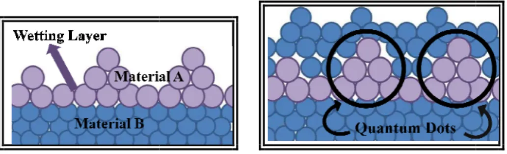
There exist several different methods to form a QD [2.3]. In this thesis it is explained the most common method to form a QD for Infrared Photodetectors (QDIPs), called Stranski+ Krastanow [2.3+2.6] growth mode.
assembled quantum dots. The c material B is denominated wetti a slow deposition is required, common techniques used nowa Epitaxy [2.1, 2.2, 2.3, 2.7, 2.8] [2.1, 2.2, 2.3, 2.9], MOCVD, br
Figure 2.2: Deposition of mate constants. The first layer of m certain critical thickness quant covered with material B.
In the other cases, like w material B, than different types Merwe in 1949 [2.2, 2.10].
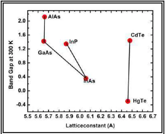
It is important to notice the materials A and B should structures, the same valences (I on). The lattice mismatch is als shows a diagram of the band ga important semiconductors alloy
2. QUANTUM DOT STRUCT
The couple of layers or so with the same lattice co d wetting layer (Figure 2.2). To form Stranski+Krastan
uired, in the order of 100 nanometers per hour. T nowadays for this kind of QD formation are Molecu
, 2.8], MBE, and Metal+Organic Chemical Vapor D D, briefly described in the following sections.
f material A over material B, for materials with different latti r of material A is coherent and is called wetting layer. After quantum dots are formed. In the right hand side, the QD are th
, like when the lattice parameter of material A is sma types of dislocations will occur. This was studied by
notice that in order to obtain good quality thin films a hould be similar. They should have equal or simila
ces (III+V semiconductors are easier to grow on III is also a crucial point in an epitaxial growth. Figure
nd gap energy as a function of the lattice constant for alloys for this thesis.
6 RUCTURES
ice constant of rastanow QDs our. The most olecular Beam por Deposition
nt lattice . After a are then
is smaller than ied by van der
7 2. QUANTUM DOT STRUCTURES
Figure 2.3: Band gap energy as a function of the lattice constant for the semiconductor systems studied in this thesis [based on Figure 8.31 from ref.2.1].
2.3 Techniques for Material Deposition
The two most important techniques to deposit materials layer by layer to produce thin films are 1) Molecular Beam Epitaxy (MBE) [2.1,2.2,2.3,2.7,2.8] and 2) Metal+Organic Chemical Vapour Deposition (MOCVD) also known as Metal+Organic Vapour Phase Epitaxy (MOVPE) [2.1,2.2,2.3,2.9].
2.3.O Molecular Beam Epitaxy
8 2. QUANTUM DOT STRUCTURES
The biggest advantages of MBE growth are the good quality of the interface materials and the possibility to control the quality of the deposited materials " , during growth. The most commonly used techniques for this purpose are Reflection High Energy Electron Diffraction (RHEED) and Mass Spectroscopy [refs]. Some other techniques like Auger Electron Spectroscopy (AES) and Low Energy+Electron Diffraction (LEED) are also used [2.1+2.3]. These techniques can be used to obtain "
control because the growth chamber is in Ultra+High Vacuum. The disadvantage of the MBE is the high cost..
Figure 2.4: Schematic picture of a MBE system. The growth takes place inside a vacuum chamber. Pure elements inside the cells pointed to the substrate are heated until sublimation. (based on Figure 8.30 from ref 2.1).
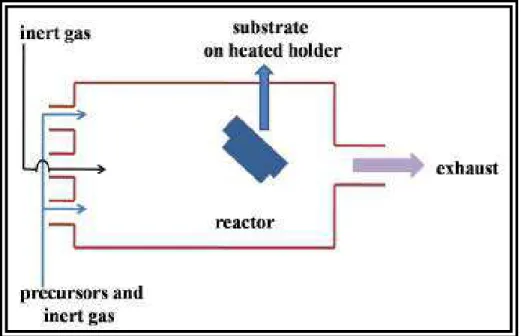
2.3.2 Metal(Organic Vapour Phase Epitaxy
9 2. QUANTUM DOT STRUCTURES
silicon (Si), the gas used is SiH4 which breaks in Si + 2H2. The Si remains on the
substrate and the H2 is collected in the exhaust. The other common gases used in
MOVPE are PH3, AsH3, Ga(CH3)3. To grow a GaAs thin film, the chemical reaction is
Ga(CH3)3 + AsH3 producing 3CH4 +GaAs. The disadvantage of this technique is the
need of highly toxic gases and the bad quality interfaces.
Figure 2.5: Schematic drawing of a MOVPE system. The growth takes place inside a reactor. Film deposition occurs after a chemical reaction. An inert gas is used to control the flux. (based on Figure 8.30 from ref 2.1).
2.4 Experimental Studies on Quantum Dots Grown by MOCVD
10 2. QUANTUM DOT STRUCTURES
Borgstrom [2.11] studied InAs QDs prepared on an InAlGaAs surface by metal organic vapor phase epitaxy. Figure 2.9a+c shows Atomic Force Microscopy (AFM) images and the corresponding height, obtained from these images of InAs QDs on InxAlyGa1+x+yAs, with increasing Al content from (a) to (c). This study demonstrates
that dots grown on material with higher Al content are smaller and that the dot density is increased. PL measurements show (Figure 2.10) that these dots luminesce at 2.1 µm and that the emission is blue shifted when the Al content is increased.
11 2. QUANTUM DOT STRUCTURES
Figure 2.10: PL spectra for InAs/ InxAlyGa1+x+yAs QDs samples. The numbers
12 2. QUANTUM DOT STRUCTURES
References:
[2.1] C. Klingshirn, # , 3rd Edition, Springer.
[2.2] P. Yu, M. Cardona, $ % &
' 3rd Edition, Springer.
[2.3] D. Bimberg, M. Grundmann, N. Ledentsov, Wiley.
[2.4] I.N. Stranski, L. Krastanow, ( )* + + '
, - K1 Abt. 2B Chemie O46, 797 (1937).
[2.5] D.J. Eaglesham, M. Cerullo, & . ! - / 64, 1943–1946 (1990).
[2.6] C. H. Chiu, Z. Huang, C.T. Poh, & . ! - / 93, 136105 (2004).
[2.7] L.Goldstein, F.Glas, J. Y. Marzin, M. N. Charasse, G. Le Roux, ) & / 47, 1099 (1985).
[2.8] R. J.Warburton, 0 & & 43, 351 (2002).
[2.9] M.Razeghi, 1 '#02 0 : ) ! & 3 ) "
3 ) "3 ) ! . Second Edition. Taylor
and Francis/CRC Press, 2010.
[2.10] F. C. Frank, J.H. Van Der Merwe, . & & )
O98, 216+225 (1949).
13 3. INFRARED DETECTORS
3. INFRARED DETECTORS
3.O Infrared Technology
14 3. INFRARED DETECTORS
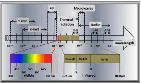
Figure 3.1: Part of the electromagnetic spectra in wavelength.
Initially, the interest in the IR region was mainly due to thermal radiation and the development of IR detectors was connected to thermal detectors [3.1, 3.2], but they are limited in sensitivity and range. Around 1860, for the first time, the IR radiation from the moon, planets and bright stars could be detected. It was only 100 years later that the IR detector technology was advanced enough to allow mapping the sky and more than 20000 IR sources were then discovered (all of them stars that could not be seen with the naked eye) [3.2].
The history of IR is reviewed in Barr’s [3.3] paper and two well+known monographs [3.4, 3.5] and in the past few decades, the IR region was intensively studied due to a wide variety of applications [3.6+3.10].
The IR detectors are subdivided in thermal detectors and photon detectors and the difference between then are the detection mechanism: in thermal detectors the absorption of the incident light results in a change of the temperature of the detector and consequently in resistance, and in photon detectors the mechanism is based on photoexcitation. This thesis is focused on quantum dot infrared photodetectors and the detection mechanism is based on photoexcitation.
15 3. INFRARED DETECTORS
image it is possible to identify and locate a health problem [3.9+3.10]. When a region of the human body is inflamed, the temperature changes and can be detected by the difference in the amount of radiation it emits, relative to a healthy area of the body. Following this line of reasoning we find several other applications in medicine, like as monitoring the healing after surgery or for the early detection of skin cancer. Still in the imaging field, we can mention applications in the industrial area to determine the level of a liquid in a tank, or even to locate obstructions in pipes. Another application that has attracted much attention recently is systems of imaging infrared heat to aid the pilots of aircraft on approach for landing.
But, mainly, IR technology was and continues to be driven by military applications [3.2]. Due to this, the technology of infrared sensors and systems is highly protected by the countries that dominate it and the purchase by Brazil of devices or sensitive equipment in that band of the electromagnetic spectrum is often difficult or even not allowed. That is why Brazil should develop its own technology for infrared detection and this involves a detailed study of semiconductor structures.
3.2 Infrared Photon Detectors
3.2.O Figure of Merit
There exist different types of IR photon detectors, which will be discussed in section 3.2.2. Due to the variety of IR detector, a few parameters are defined to make possible the comparison of the performance of these devices and, of course, to make a quantitative characterization of different detectors. Here, we focus on photoconductive photon detectors, where the detection mechanism is based on photoexcitation. The incident radiation excites an electron to the continuum of energy levels in the conduction band, this electron drifts towards the collector and a photocurrent is created.
16 3. INFRARED DETECTORS
,
(3.1)where is the elementary charge, is the photon energy absorbed with an efficiency and is the gain (Figure 3.2). The gain is the capacity of the detector to increase the output signal from the input. It is defined as:
,
(3.2)where !" is the carrier lifetime and #$ is the carrier transit time. From this equation one can conclude the importance of both quantities. The carrier lifetime is the average time that the carrier takes to recombine. The transit time is the time that the electron needs to cross the active region and it is larger for thicker samples.
Figure 3.2: Scheme of a QDIP of thickness t. The incident radiation is absorbed with efficiency η and generates a photocurrent PC.
17 3. INFRARED DETECTORS
The sensitivity can be quantified by measuring the noise
&
'(&)*. In the case that the noise bandwidth is as large as the generated signal, it would be impossible to discriminate both. Different mechanisms can contribute to the noise [3.1, 3.2], like temperature noise, photon noise, generation+recombination noise+,
and others. In the case of Quantum dots Infrared Photodetectors, the last one is the dominant noise mechanism [3.14] and can be estimated by measuring the dark current-
.
The
+,
is a result of the generation+recombination rates of the electrons between different energy states of the material. It is a statistical process that depends on too many parameters and is very difficult to calculate. The dark current-
is the current that flows without input signal. This current can be generated by mechanisms like thermionic emission, thermal assisted tunneling and sequential tunneling. These mechanisms depend on the structure and on the bias and temperature of operation.The relation between the dark current and the generation+recombination noise is given by:
+,
.
4* ∆1
-
(3.3)
where is
*
electron charge, is the gain and∆1
is noise bandwidth.Actually, the figure of merit of a photodetector which is more important is the so+called detectivity D, which is a quantitative value for the signal to noise ratio of the device at a given bias and temperature, for a specific wavelength [3.13 + 3.16]. In the literature it is referred as the inverse of a quantity defined as noise equivalent power
23
.
4
5
678
,
9
(3.4)
The specific detectivity
4
∗ is then defined as the detectivity of a photodetector with an area of 1 cm2 and an electrical bandwidth of 1 Hz.
4
∗
,
18 3. INFRARED DETECTORS
where
>1
is the bandwidth and=
is the detector area. The unit for4
∗ is the 4 (cm x Hz ½ /W) in honor to R. Clark Jones who defined this magnitude [3.15, 3.16].3.2.2 Types of Infrared Photon Detectors
According to Martyniuk [3.17] the majority of infrared photon detectors in use nowadays can be divided into five classes:
i) direct band gap semiconductors (InSb, InAs, HgCdTe or MCTs, etc),
ii) extrinsic semiconductors (Si:As, Ge:Hg, etc), iii) superlattice (GaAs/AlGaAs QWIPs),
iv) Silicon Schottky barrier (PtSi, IrSi) and v) quantum dots (InAs/GaAs, InAs/InP,etc).
19 3. INFRARED DETECTORS
Figure 3.3: Band gap energy and lattice constant for important material for infrared photodetectors
In general, in QWIPs the transition generated by the absorption of the radiation is intraband. It occurs in the conduction band between a bound quantum well state and a state in the continuum. This makes QWIPs more selective devices when compared to MCTs detectors. The drawback of QWIPs is the presence of selection rules which forbid the absorption of normal incident light. This makes QWIPs not as efficient and they demand the use of diffraction gratings on the top of the device or some other artifact to change the direction of normal incident radiation. Besides that, QWIPs only work at low temperatures.
20 3. INFRARED DETECTORS
as showed in sub+section 3.2.1 of this thesis. Finally, the dark current in QDIPs is expected to be lower [3.27].
Since the proposal of these new structures, a lot of attention has been devoted to them [3.28+3.34]. The intense study on self assembled quantum dots is in part due to their potential to suppress other material systems for infrared photodetection. Figure 3.4 presents a graph [3.17] of the calculated detectivity, for different types of photodetectors operating at 5 µm and in Figure 3.5 the predicted detectivity for photodetectors operating at 10 µm [3.17]. The assumed quantum efficiencies are indicated in the figures. Theoretical estimations for QDIPs are carried out assuming low quantum efficiency 2% (often measured in practice) and high efficiency of 67%. The last value is typical for HgCdTe photodetectors. From this graph we can conclude that the detectivity of high efficiency QDIPs are comparable to the performance of HgCdTe photodetectors. We can also notice that AlGaAs/GaAs QWIPs have better performance than extrinsic silicon photodetectors.
21 3. INFRARED DETECTORS
Figure 3.5: Predicted detectivity as function of temperature for different types of photodetectors operating at 10 µm [3.17].
3.3 Stand out works on Quantum Dots Infrared Photodetectors
The most studied system in the literature for infrared photodetection applications are InAs/GaAs. In this thesis I report results on the InAs/InP QD based system. Even though they have the same quantum dot material, they differ in three important aspects, which lead to different electronic and optical properties of the two systems [3.35]:
i+ InAs/InP has much smaller lattice mismatch (3%) when compared to InAs/GaAs (7%) (See picture in section 1.3);
ii+ InAs/InP has a weaker confining potential for electrons, but stronger for holes;
22 3. INFRARED DETECTORS
In addition to new materials, new concepts and innovative structures also need to be investigated. An interesting proposal, presented in 2006 to increase the efficiency of photodetectors based on intraband transitions, is the so+called Tunneling Quantum Dot Infrared Photodetector (T+QDIP) [3.33]. Double AlGaAs/InGaAs barriers are inserted, generating resonant levels and blocking the dark current. The transport of carriers is done by tunneling. Figure 3.6 shows the potential profile of the structure studied by Bhattacharya [3.33]. This structure, grown on a GaAs substrate, has a spectral response around two frequencies (6 cm and 17 cm) and has obtained good results for detectivity at room temperature for 17 cm.
Figure 3.6: Conduction band diagram of a Tunneling QDIP structure [3.33] and the calculated energy levels. The electrons that are not at the resonant level are blocked by the barrier.
In these T+QDIP structures the tunneling probability for the excited carriers in the resonant level is near unit while all the other carriers are blocked by the barrier. In this sense it is possible to introduce a high potential barrier for the thermal excitations with lower photo excitation energy. As a result, the operating temperature can be significantly increased.
23 3. INFRARED DETECTORS
dots in the well, D+WELL, with high responsivity and low dark current. Some photocurrent results are shown in Figure 3.7.
Figure 3.7: Photocurrent results obtained by Lim et al. for D+WELL samples. In (a) is presented the photocurrent as function of temperature, measured at a bias voltage V = +1 V. In (b) he shows the photocurrent response for V = + 5 V and V = + 2 Vas function of temperature. In the inset is presented the results at room temperature measured with V=+2V and V=+1 V.
Greater understanding of the involved mechanisms in intraband transitions of QD structures is required for planning more efficient devices. Despite the intense effort in the last two decades, the physics of self+assembled quantum dot structures for mid+ infrared photodetection implementation has several unanswered questions.
3.4 How to Produce a QDIP
24 3. INFRARED DETECTORS
Figure 3.5: Quantum dot infrared photodetector scheme.
The procedure starts by the definition of all the parameters of the structure, which depends on the kind of detector we want to produce. The structure influences the spectral response of the detector, not only the wavelength of the detection but also the type of detector, narrow or broad band. The material of the structure also influences the response of the device, since different materials have different band offsets and different optical properties. The thickness and height of the barrier also affect the detection wavelength and the magnitude of the dark current.
Excluding the setting of the structure parameters, we could divide the process into two parts. The first one consists of the sample growth and characterization, and the second part is the device fabrication and characterization.
25 3. INFRARED DETECTORS
influences the detection wavelength. In the case of intraband bound+to+continuum transitions, for larger dots the ground state is lower in energy, which gives a shorter operation wavelength. The density and uniformity of the dots affect the detectivity of the device. The higher these latter parameters are, the higher is the responsivity. The doping of the dots also has an effect on the responsivity and dark current.
To characterize the QD samples several techniques like Atomic Force Microscopy + AFM, Transmission Electron Microscopy TEM, absorption and photoluminescence + PL are generally used. The samples studied here were analyzed by all these four techniques. For AFM measurements, samples with uncapped dots were prepared. For the absorption measurements, we grew samples with 20 periods and without contact layers.
26 3. INFRARED DETECTORS
References
[3.1] M.A. Kinch, 4 ' 29, 6 (2000).
[3.2] A. Rogalski, J. Antonszewski, L. Faraone, 4 ) & O05, 091101 (2009).
[3.3] E. S. Barr, ) 4 & 28, 42 (1960).
[3.4] R. A. Smith, F. E. Jones, R. P. Chasmar, 1 ' . Clarendon. Oxford, (1958).
[3.5] P.W. Kruse, L.D. McGlauchlin, R.B. McQuistan, 1 & Wiley. New York , (1962).
[3.6] P. Norton, J. Campbell, S. Horn , D Reago, 4130, 226 (2000).
[3.7] M. Z. Tidrow, W. A. Beck, W. W. Clark, H. K. Pollehn, J. W. Little, N. K. Dhar, P. R. Leavitt, S. W. Kennedy, D. W Beekman, A. C. Goldberg, W. R. Dyer, # " . ! - 7, 283 (1999).
[3.8] M. N. Abedin, T. F. Refaat, I. Bhat, Y. Xiao, S. Bandara, S. D. Gunapala, 5543, 239 (2004).
[3.9] P. McCarley, 4288, 1 (2001).
[3.10] J. T. Caulfield, 56 ) &
. + * , IEEE, New York, 2003.
[3.11] F. Capasso, C. Gmachl, R. Paiella, A. Tredicucci, A. L. Huntchinson, D. L. Sivco, J. N. Baillaargeon, A. Y. Cho, H. C. Liu, 4 1
6, 931+947 (2000).
[3.12] V. W. S. Chan, Optical space communication, IEEE J. Select. Topics Quantum Electronics 959 + 975 (2000).
[3.13] H. Lim., W. Zhan, S. Tsao, T. Sills, J. Szafraniec, K. Mi, B. Movaghar, M. Razeghi, & ! - 7 72, 085332 (2005).
[3.14] D.Long, & 7, 169+170 (1967) [3.15] R. C Jones, . 2, 9+12 (1957).
[3.16] R. C. Jones, 4 # & ) 50, 1058 (1960).
[3.17] P. Martyniuk, A Rogalski, , 32, 89
(2008).
[3.18] M. Aria, M. Zandin, J. G. Pasko, J. Bajaj, L. J. KozlowskI, W. E. Tennant E R. E. De Wames, Proc. SPIE 2274, 2+16 (1994).
27 3. INFRARED DETECTORS
[3.20] P. Tribolet, J. P. Chatard, P.Costa e A. Manissadjian, 4 0 & 3 -
O84, 1262+1271 (1998).
[3.21] B.F. Levine, 4 ) & . 74, R1+R81 (1993).
[3.22] M. Razeghi, M. Erdtmann, C. Jelen, F. Guastavino, G. J. Brown, Y. S. Park, , Infr. Phys. and Technol. 42, 135+148 (2001).
[3.23] E. Towe e D. Pan, IEEE J. Selec Top. Quantum Electr. 6, 408+421 (2000). [3.24] V.Ryzhii, , Semiconductor Science and Technol. OO, 759 (1996).
[3.25]J. Phillips, K. Kamath, and P. Bhattacharya, ) & / . 72, 2020 (1998)
[3.26] R. Ferreira, G. Bastard, Appl. Phys. Lett. 74, 2818 (1999).
[3.27] V. Ryzhii, V. Pipa, I. Khmyrova, V. Mitin, M. Willander, Jpn. J. Appl. Phys. 39, 12B L1283 (2000).
[3.28] H. Lim, S. Tsao, W. Zhang, M. Razeghi, Applied Physics Letters 90, 131112 (2007).
[3.29] J. Phillips, P. Bhattacharya, S. W. Kennerly, D. W. Beekman e M. Dutra, IEEE J. Quantum Electron. 35, 936 (1999).
[3.30] M. R. Matthews, R. J. Steed, M. D. Frogley, C. C. Phillips, R. S. Attaluri, S. Krishna, Appl. Phys. Lett. 90, 103519 (2007).
[3.31] V. M. Apalkov, Physical Review B 75, 035339 (2007). [3.32] R. J. Warburton Comtemporary Physics 43, 351 (2002).
[3.33] G. Ariyawansa, A.G.U.Perera, X.H.Su, S. Chakrabarti, P. Bhattacharya, Infrared Physics and technology 50, 156 (2007).
[3.34] Q. Han, X. H. Yang et al., “1.55 µm GaInNAs resonant+cavity+enhanced photodetector grown on GaAs”, Applied Physics Letters 87, 111105 (2005); para um artigo de revisão anterior veja M. S. Unlu, S. Strite, . ! &
! , Journal of Applied Physics 78, 607 (1995).
28 4. THEORETICAL MODELING
4. THEORETICAL MODELING
4.O Introduction
Theoretical calculations of the energy levels and the oscillator strengths of the several possible transitions are essential for the full understanding of the physics behind the devices based on semiconductor quantum dots. If we want to calculate the electronic band structure to describe a semiconductor, all we have to do is to solve Schrödinger’s equation for the system.
To calculate the energy levels in three+dimensional quantum confinement structures, José Maria Villas Bôas, during his short post+doctoral work at 8 !
$ ' 3 – UFMG, and Carlos A. Parra Murillo, during his master studies at UFMG, developed a computer code based on the method proposed by Gangopadhyay and Nag [4.1]. In this chapter I briefly explain the method. More details are available in Carlos A. Parra Murillo’s master thesis [4.2] and in the original paper.
4.2 Description of the Method
To calculate the energies values and eigenfunctions of the quantum dot photodetector structures, we must solve the Schrödinger’s equation in the effective mass approximation for the system:
?@A BCDB EA BCDB (4.1)
where ?@is the Hamiltonian operator of the complete system.
We consider the single+particle Hamiltonian H, which can be written as:
− GH I
29 4. THEORETICAL MODELING
where S" is the free+electron mass, S∗ J P KKLM is the effective electron mass for the structure , and V is the potential.
We can write CJ P KKLM in a convenient basis of functions:
CJ P KKLM T U J P KKLM (4.3)
The basis functions are the solutions V?@WA B DB E A B DBX of the problem consisting of one particle with effective mass confined in a large cylinder of radius . and height / and a potential V = 0, if r < R, and infinity otherwise (Figure 4.1). For this problem we find that:
E I YZ .I G
Z[Z \Z +]^
Z
,ZO (4.4)
Figure 4.1: Schematic representation of 9: used to
construct the basis for 9.
The second step consists of studying a quantum dot structure placed inside a cylinder like the one in Figure 4.1. For this we solve the eigenvalue equation 4.5, where H contains all the information about the quantum dots and barriers.
30 4. THEORETICAL MODELING
For this purpose we implemented the method introduced by Gangopadhyay and Nag [2]. If we substitute equation 4.3 in equation 4.2 and multiply the result by _I_∗ and integrate in all the space we obtain a characteristic equation:
TJ=`I` `, I − Eb _ bI_Ib _ M U`I` ` 0 (4.6)
The matrix elements are given by:
=`I` `, I − dfg$h"eR G _I_∗ ∙II∗∇. I − _I_∗ R I O (4.7)
It is possible to reduce the expression of the matrix elements integrating by parts the left term in the parenthesis, so we obtain:
=`I` `, I − dfg$h"eR GI
I∗∇ _I_∗ ∙ ∇ I − _I_∗ R I O (4.8)
To solve the equation above it is important to note that: 1) the effective mass is a function of and ,
2) the structures studied here have discontinuous effective mass, and, 3) the structures studied here have discontinuous potential functions at the
interfaces between two different materials.
To solve equation 4.8 we consider the following:
i) We integrate with m*(r, z) = mb and V (r, z) = Vb over the external
cylinder because ψ is null outside the cylinder. This gives us:
j= _I_ _ Ihk l
Im,nm G I Im G
]Z^ ,Z +
Z[Z
\Z O + RoO b _ bI_Ib _ (4.9)
31 4. THEORETICAL MODELING
quantum dot parameters, i.e, m∗(r, z) = mQD e V (r, z) = VQD (see Fig.
4.2), this gives:
j=p- _I_ _ I lIm,nm− j=p- _I_ _ I lIqr,nqr d eRp- sIIqr− I
Imt ∇ _I_
∗ ∙
∇ I + d eRp- VRp-− Ro X _I_∗ I (4.10)
Figure 4.2: Schematic representation.
iii) so, the matrix element A can be written as:
= _I_ _ Iu $ j=h _I_ _ Ik lIm,nm+ j=p- _I_ _ I lIm,nm− j= _I_ _ Ip- lIqr,nqr (4.11)
In our project, we studied several complex structures with quantum wells, barriers and quantum dots inserted in the structure. To compute real structures we generalize this process. So, if the structure consists of N dots and M wells, the matrix element is given by (see Figure 4.3):
= _I_ _ Iu $ j=h _I_ _ Ik lIm,nm+
T sj=2vW p- _I_ _ I lIm,nm− j=p- _I_ _ I lIqr,nqr t +
32 4. THEORETICAL MODELING
Figure 4.3: Schematic representation of 9: used to construct the basis for 9 in the case of
several dots and wells in the structure.
iv) Up to now I show how to solve the matrix elements for an arbitrary quantum dot shape. Here we show how to include the quantum dot shape in the equation. For this, we go back to equation 4.12 and modify the integral limits and in this way it is possible to change the dot shape. The most common shapes are shown is Figure 4.4. In this picture we show the curve that generates the quantum dot by the rotation of this plane along the z+axis. This defines the upper limit of the integral.
Figure 4.4: Different quantum dot (QD) shapes. In (a) cone shaped QD, in (b) cylinder shaped QD and in (c) lens shaped QD.
For the QD shapes shown in Figure 4.4 the upper limit of the integral is wrriten as:
33 4. THEORETICAL MODELING
zJPM WG1 − #
,|O (4.13) 2) Cylinder shaped QD:
zJPM } W, 0 ≤ P ≤ W
0, (• *P€&)* B (4.14) 3) Lens shaped QD:
z JPM W•1 −,#Z
|Z (4.15)
v) The next important parameter to compute is the oscillator strength for each pair of levels, which allows us to find the most probable intraband transitions in the system, due to absorption of incident radiation. To compute this parameter the most frequently used formula is:
1J‚_, ƒ_; ‚, ƒM .I∗
YZ JE`,]`− E ,]M A …‚_, ƒ_APLA‚, ƒ† A. 4.16)
Its use depends on the system of units used, but what are really important are the relative values between the transitions. The difficulty in this point is to calculate the matrix element of the position vector PL. In our case we have that:
…‚_, ƒ_APLA‚, ƒ† ‡ ePLn …‚_, ƒ_APLAPL† …PLA‚, ƒ† ˆePL
n V‰Š‹ + Œ•‹ + zƒŽX …‚
_, ƒ_APL†…PLA‚, ƒ†
‡ ePLn V‰Š‹ + Œ•‹ + zƒŽX C∗`,]` JP, •, zM C ,] JP, •, zM (4.17)
where …PLA‚, ƒ† C ,] JP, •, zM are the eigenfunctions of our problem.
34 4. THEORETICAL MODELING
References
[4.1] S. Gangopadhyay, B. R. Nag, Nanotechnology 8, 14 (1997).
35 5. EXPERIMENTAL TECHINIQUES
5. EXPERIMENTAL TECHINIQUES
5.O Fourier Transform Infrared Spectroscopy
36 5. EXPERIMENTAL TECHINIQUES
Figure 5.1: Schematic picture of the FTIR setup for absorption measurements.
37 5. EXPERIMENTAL TECHINIQUES
Figure 5.2: Setup for photocurrent measurements
5.O.O Sample Processing for Photocurrent Measurements
All the samples were processed at the Technical University of Vienna (TU+ Wien) during a one year stay (Sandwich PhD scholarship – SWE) in 2008.
The processing of the samples for photocurrent measurements consists on the device fabrication. It is, basically, a sequence of steps to build up the with an optical window and also to fabricate the electrical contacts (Figure 3.5). This last step includes the deposition of metal layers to contact the wires. The area of our devices is around 9 x 104 µm², therefore the fabrication procedure is very delicate.
There exist different methods and recipes for processing the devices, which depend on the device size, thickness and material, and also on the clean room equipment facilities. The processing of the samples studied here was done by conventional photolithography and dry etching. The sequence of steps and parameters are described in this section.
38 5. EXPERIMENTAL TECHINIQUES
The second step is the transfer of the pattern of the mask to the SiN. For that we use conventional photolithography with the 5214 Photo+resist. We deposit the resist on the sample located in a spinner, rotating at 10 thousand rotations per minute during 35 seconds, to achieve a 1.1 µm thickness. Then we bake the resist for 1 minute at 120°C. In the mask aligner, we illuminate the sample during 4.5 seconds, and in the sequence we develop for 30 seconds in AZ 351 solution. A schematic picture of the sample at this point of the processing is shown in Figure 5.3 b).
The following step is the etching of the SiN, to transfer the pattern of the resist layer to the SiN. The etching was done with a Reactive Ion Etching (RIE) system with a step and strike pressure of 15 and 40 mtorr, respectively and power of 60 W at 25 oC. The gas used was SF6 at a flux of 40 sccm. After this step, the sample looks like shown
schematically in Fig. 5.3 c).
To start etching the sample, to build up the mesas, it is necessary first to remove the resist layer. This procedure was done in a 1 plasma oxidation machine, which removes only organic materials. See Fig. 5.3 d)
The sample etching was done at 250 0C in a Reactive Ion Etching (RIE) setup,with SiCl4 and Ar with a flux of 5 and 40 sccm. The step and strike pressures were 2 and 40 mtorr respectively and the power was 200 W (Fig. 5.3 e).
The next procedure is to remove the SiN and prepare the sample for metallization. The SiN was removed in the same way it was etched (Fig. 5.3 f).
The following photolithography, to select the metallization area, was done with a negative resist, MAN 440, spinning the resist at 6000 rotations per minute during 30 seconds. The sample was warmed for 5 minutes at 95°C before being taken to the mask aligner. The exposure time in the mask aligner was 60 seconds. The developer used was MAD 333 for 70 seconds.
39 5. EXPERIMENTAL TECHINIQUES
Figure 5.3: Illustrative picture of the sample for all the process steps.
5.O.2 Sample Processing for Absorption Measurements
For absorption measurements the samples were processed in a waveguide geometry to increase de optical pass inside the sample and consequently to achieve a better signal to noise ratio. Still aiming a better signal, we used samples with 20 periods in the active region (for photocurrent measurements the samples had only 10 periods).
The waveguide geometry consists on polishing the facets of the samples in 45º and focus the light on this facet. Thus the incident radiation suffers multiple internal reflections (Figure 5.4), increasing the optical path inside the material.
Figure 5.4: waveguide geometry.
40 5. EXPERIMENTAL TECHINIQUES
In order to polish a waveguide the samples were fixed on a well designed metallic sample holder.
5.2 Current(Voltage Measurements
The current+voltage (IV) measurements were done with a HP4155B parameter analyzer. The samples were mounted inside an optical cryostat to perform temperature dependent measurements. The measurements were performed under dark condition, from V = +5 V to V= +5 V in steps of 10 mV and the maximum current (compliance) was 100 mA.
Figure 5.5 shows the IV curves for the QD+undoped sample described in section 6.2 and in Figure 5.6 the IV curves for the sample 6.3.
41 5. EXPERIMENTAL TECHINIQUES
42 5. EXPERIMENTAL TECHINIQUES
References:
6. RESULTS
43
6. RESULTS
6.O Introduction
6. RESULTS
44 In the sections below I present some physical processes involved in the structures developed for this thesis.
6.2 Evidences of Intraband Auger Process in Quantum Dot
Infrared Photodetectors
For most of the QD structures used for infrared photodetection, the optical transitions are intraband and occur between two bound states or a bound and a quasibound state. The physical process behind the carrier extraction from the excited states to generate the observed photocurrent (PC) is often attributed to thermal excitations, even for deep final bound states [6.4+6.7]. Another mechanism to extract the carriers to the continuum, where they can contribute to the PC, is via an Auger process. This physical phenomenon is based on energy exchange between electrons. When an electron in a high energy level falls to a lower energy level, the excess energy can be transferred to a second electron. If this energy is enough to promote it to the continuum, this second electron, the Auger electron, might be collected contributing to the PC.
The importance of Auger processes in semiconductor quantum dot structures has already been claimed in the 90’s in a detailed theoretical study [6.8]. More recently, the interband PC spectra of InAs quantum dots embedded in an InP matrix were explained by the involvement of Auger processes [6.9] in undoped layers and n+ and p+type doped InGaAs quantum dots were theoretically investigated [6.10]. However, the first experimental evidence of the Auger effect on intraband transitions in QDIPs was investigated by our group [6.11]. In this section I present our results that demonstrate that Auger processes seem to play a fundamental role in generating an intraband PC.
In order to observe the Auger effect in intraband transitions in QDs, samples were designed in such a way that there awere several bound states available inside the dot. This can be achieved by growing relatively large dots.
6. RESULTS
45 content. The InAs QDs are then deposited for 5.5 s at 520°C and annealed in an arsine atmosphere for 12 s. They are covered by a 13 nm thick InP layer while the temperature is ramped up to 600°C. This sequence is repeated 10 times. A last 109 nm thick layer of the quaternary material is then grown and finally a 250 nm +doped InGaAs contact layer is deposited. The doping level at the contact layers is 1.0 x 1018 cm+3. All ternary and quaternary layers are grown at 600°C. The QD samples were grown with three different doping levels: one nominally undoped sample and 2 samples with a doping which corresponds to approximately 2 and 4 electrons per dot, respectively. The schematic conduction band potential profile and scheme of the samples are presented on Figure 6.1.
Figure 6.1: a) shows schematically the layers material and thickness along the growth direction and in b) the conduction band profile of one period of the active region.
Figure 6.2: AFM (left side) a
To characterize the dev Fourier Transform Infrared Spe photocurrent spectra at 5 K for light and no external bias. A undoped sample. The sample is and carrier diffusion from the intraband transitions can occur doped samples. The broadeni inhomogeneous size of the qu ground state lies deeper in ener populated, originating a narrow electrons inside and this small d the PC peak.
6. RE
side) and TEM (right side) images of the quantum dot structures
e devices, photocurrent measurements were perform ed Spectroscopy (FTIR) (see chapter 5). Figure 6.3
K for the investigated samples measured with normal as. A narrow PC peak is observed around 190 meV
ple is nominally undoped, but the presence of residua m the contacts lead to a population inside the QD occur. A stronger and broader signal was observed oadening of the PC peak with the doping is du
he quantum dots all over the structure. For larger Q n energy, so for the undoped sample, only part of thes
arrow PC peak. For the doped ones, also the smaller d small difference in energy is responsible for the broad
6. RESULTS
46
ctures.
6. RESULTS
47
Figure 6.3: Photocurrent spectra for all three samples. The inset shows the absorption spectra around 200 meV for the undoped and high doping samples.
6. RESULTS
48
Figure 6.4: Absorption measurements for the undoped sample (red spectra) and the high
doped sample (blue spectra).
6. RESULTS
49
Figure 6.5: Calculated energy levels superimposed on the conduction band profile of one period of the active layer of the samples. The arrows represent the transitions with the highest oscillator strength.
6. RESULTS
50
Figure 6.6: Schematic picture of an intraband Auger process.
6. RESULTS
51
Figure 6.7: Photocurrent measurements at different temperatures. The spectra are shifted vertically
for clarity.
6. RESULTS
52
Figure 6.8: Photoluminescence and interband photocurrent measurements and a schematic picture of an interband Auger process.
The difference between the intraband and interband Auger effect is that for the first one it is necessary to have two electrons in the excited states, in the same quantum dot and essentially at the same time. Even though it can appear improbable, it is necessary to remember that the FTIR measurements are performed with a broadband source, implying that several different absorptions can occur simultaneously.
6. RESULTS
53 A second configuration for Auger scattering can be found if the effect of the persistent device current is taken into account. As the devices were operated in current+ mode, a photocurrent was present even without bias applied due to an intrinsic electric field. When the electrons pass through the QD layers some of them can relax into the dots. If an electron relaxes into a dot with an excited electron inside, this electron can be promoted to the conduction band continuum due to Auger scattering and will contribute to the PC.
The detectivity of these devices was estimated. Figure 6.9 shows the results as function of bias and temperature. One can clearly conclude that the low doping sample shows a better performance, especially at low temperatures and low applied bias voltages. For the responsivity measurements we use an InAs filter to avoid interband population. To calculate the noise we considered the generation+recombination noise
+,
which is the dominant noise mechanism in QDIPs and can be estimated bymeasuring the dark current
-
(see section 3.2.1).Figure 6.9: Detectivity as function of temperature (left hand side) and bias voltages (right hand side) of all
three samples.
6. RESULTS
54 strongly suggest that an Auger process can produce a significant current. Photoluminescence together with interband photocurrent further supports this attribution. The reported results indicate that quantum dot structures can be designed for the implementation of selective photodetectors based on bound+to+bound transitions, with well defined, sharp, operation energies.
6.3 Very Narrow Band QDIP Operating at O2 µm
Due to discrete energy levels, QDs structures should lead to narrower transitions, desirable for achieving high selective devices. Therefore QDIP structures should be ideal to distinguish two different gases with absorption at wavelengths in the mid infrared which are very close to each other or for sharp temperature discrimination for imaging. For the latter application, devices with operating wavelengths in the 9+12 m range should be employed since they correspond to maximum of the thermal emission at room temperature and peak widths as narrow as possible are desirable. In this section I present the development of an InGaAlAs/InGaAs/InGaAlAs/InAs/InP QDIP structure where an InGaAs quantum well is coupled to the InAs quantum dots which operates around 12 microns with a photocurrent peak as narrow as 5 meV (5% for λ/λ). The absorption occurs between deep quantum dot states and the current generation, which is mediated by Auger scattering [6.11], relies on tunneling through an adjacent quantum well.
The investigated QDIP structures were grown by metalorganic vapor phase epitaxy (section 2.3.2). The active region of the device consists of 10 periods of a 99 nm thick InGaAlAs layer with 16% Al content lattice matched to the InP substrate on which a 10 nm In0.53Ga0.47As quantum well is grown followed by a 3 nm quaternary barrier on
top of which the InAs quantum dots are nucleated. The dots are finally covered by an InP barrier with three different thicknesses, namely: 10, 13 and 16 nm. Finally, another 99 nm thick quaternary layer is deposited (See picture 6.10). The entire periodic structure is grown between +doped In0.53Ga0.47As contact layers. The quantum dots are
6. RESULTS
55
Figure 6.10: a) Sample structure where the thickness of the InP barrier X = 10, 13 and 16 nm. b) The scheme of the conduction band profile for negative and positive bias.
6. RESULTS
56
Figure 6.11: Photocurrent for the samples with 10 nm (left side) and 13 nm (right side) thick InP barrier
as function of bias. For the samples a peak at 12 microns is observed at positive bias.
For the sample with the thickest InP barrier (Figure 6.12) we do not observe the narrow peak at 12 microns. For negative bias a broad peak is measured for all three samples.
Figure 6.12: Photocurrent for the 16 nm InP barrier.
The 12 microns peak has a full width at half maximum of less than 5 meV, corresponding to a λ/λ of only 5 %, indicating that a bound to bound transition is involved. To understand the observed PC we used the method described in chapter 4 to calculate the energy levels for the structures and the oscillator strengths for all possible
6. RESULTS
57 transitions. The most important energy levels for angular momentum quantum numbers m=0 (solid lines) and m=1 (dashed lines) are shown in figure 6.13a, superimposed on the QD structure potential profile for positive bias. For an energy of 100 meV (12 microns) the most probable transition is from the lowest energy level to the first excited state both with m = 1, namely state (0,2) to state (1,3). Figure 6.13b shows the probability density in the ρ plane, where is the growth and ρ is the QD base radius directions, for these two states. One clearly sees that both the (0,2) and (1,3) states are fully localized in the QD. The absorption involved in the 100 meV PC peak is attributed to the optical transition between these two states. The localized nature of these energy states explains the exceptionally narrow generated peak.
6. RESULTS
58
Figure 6.13: Relevant energy levels and the optical transitions with the highest oscillator
strength for the 13 nm InP barrier structure.
To finalize the section, Figure 6.14 shows the detectivity for the 10 nm thick InP barrier which shows a better performance at low temperature operation.
Figure 6.14: detectivity for the 10 nm thicker InP barrier as funcition of
temperature.
6. RESULTS
59 m. The identification of the energy levels involved in the PC generation processes was made with the help of two independent calculation methods. The energy levels involved in the absorption are fully localized in the quantum dots. In order to generate the observed photocurrent, the electrons first reach the conduction band of the quaternary material via the adjacent InGaAs quantum well either by an intraband Auger effect or by the absorption of a second photon (which mechanism is yet to be determined) and finally tunnel through the thin InP barriers. Enhanced photocurrents are expected if the QDs are covered with the quaternary material, avoiding the last tunnelling step. This would require improvements in the crystal growth of the InGaAlAs layer under a varying growth temperature.
6.4 Dual Sign Photocurrent in Quantum Dot Structures for
Infrared Photodetection
The photocurrent generation in quantum dot infrared photodetectors (QDIPs) involves, at least, 4 mechanisms. First the absorption of the incident light to photoexcite a carrier, then the extraction of the carrier from the quantum dot, followed by the transport of this carrier along the structure and, finally, the collection of the carrier to generate the PC trough an external circuit [6.15]. The understanding of these mechanisms can guide us in optimizing the detectivity of a photodetector, which is directly proportional to the photocurrent intensity (responsivity). The ideal case would be 100% efficiency, where all the excited electrons are collected, contributing to the PC. It is important to mention that the responsivity of quantum dot structures for infrared photodetectors is expected to be higher when compared to quantum well structures due to the longer life time of the carriers [6.16]. In this section we investigate how the structure around the quantum dot can influence the mechanisms of carrier extraction and consequently the photocurrent signal.
6. RESULTS
60 continuously varying the Al content from 20% to 11% so as to generate a half parabolic+shaped potential well (PQW). This graded layer is kept lattice matched to the substrate by varying the In and Ga concentrations accordingly. Then a 3 nm thick layer of InGaAlAs was deposited, on top of which the InAs QDs were nucleated. An 8 nm thick layer of InP, acting as a second barrier, was used to cover the dots. The second half of the parabolic quantum well was then grown varying the Al content of the quaternary material from 11% to20%, keeping the material lattice matched. Finally 99 nm of lattice matched InGaAlAs with 20% Al was deposited completing the first period. Ten periods like this one were grown. Bottom and top electrical contact layers, made of In0.53Ga0.47As heavily doped (n = 2 x 1018 cm+3) were deposited as shown
schematically in Fig. 6.12.
For the second structure (Sample B in figure 6.16) a lattice matched InGaAlAs layer with 20% Al was first deposited on the InP substrate, followed by a 4 nm thick In0.52Al0.48As barrier layer. Then a 3 nm layer of lattice matched InGaAlAs also with
20% Al was grown on top of which the InAs quantum dots were nucleated and covered by 8 nm of InP. A 3 nm thick layer of In0.52Al0.48As was then deposited on top of which
an In0.53Ga0.47As quantum well was grown. As the barrier material for the QW, a 4 nm
In0.52Al0.48As barrier layer was grown. The thin In0.52Al0.48As barriers were grown in
order to achieve lower dark current. Finally, a 99 nm layer of 20%Al, lattice matched InGaAlAs was deposited, to complete the first period. As for sample A, this structure had ten periods sandwiched between In0.53Ga0.47As heavily doped (n = 2 x 1018 cm+3)
6. RESULTS
61
Figure 6.15: Schematic diagram of the layer sequence and conduction band profile of Sample A. On the left hand side the material composition and the thickness of each layer is specified.
Figure 6.16: Schematic diagram of the layer sequence and conduction band profile of Sample B. On the left hand side the material composition and the thickness of each layer is specified.
The photocurrent response was measured with Fourier transform infrared spectroscopy (FTIR) as a function of bias and temperature (Chapter 5). The
! ! curves were performed with a parametric analyzer.
6. RESULTS
62 in intensity and dominates the spectrum for the highest bias values. Close to zero bias, photocurrent in both directions is observed, at different values of photon energy. This dual behavior was also studied by Schneider in a previous work on quantum well structures [6.17+6.19] and it was shown to be related to the asymmetry in the structure. In our case, the InP barrier, that covers the QDs, promotes a preferential escape direction for the electrons that is in the opposite direction of the barrier, since the tunneling probability is not so high.
To make a detailed study of this behavior a second structure was developed (Figure 6.16). In this one we included a quantum well after the InP barrier. The PC spectra of the sample as a function of the external applied bias voltage at low temperature are shown in Figure 6.18. Two narrow and intense peaks, one at 190 meV and a second one at 230 meV can be clearly identified. A third, weaker peak, is observed at 300 meV. As the external bias voltage is decreased, for values very close to zero bias the same dual sign photoresponse, as seen in Sample A, is measured. For the same value of external applied bias voltages, current flows in both directions.
6. RESULTS
63
Figure 6.18: PC spectrum for sample B as a function of the external applied bias voltages.

![Figure 2.3: Band gap energy as a function of the lattice constant for the semiconductor systems studied in this thesis [based on Figure 8.31 from ref.2.1]](https://thumb-eu.123doks.com/thumbv2/123dok_br/15786369.131829/17.918.202.737.121.574/figure-function-lattice-constant-semiconductor-systems-studied-figure.webp)

![Figure 2.9: 2 x 2 µm 2 AFM images and corresponding dot height on In x Al y Ga 1+x+ y As with (a) y = 0; (b) y = 0.11; (c) y = 0.16 [2.11]](https://thumb-eu.123doks.com/thumbv2/123dok_br/15786369.131829/20.918.223.702.354.1046/figure-µm-afm-images-corresponding-dot-height-al.webp)
![Figure 2.10: PL spectra for InAs/ In x Al y Ga 1+x+y As QDs samples. The numbers represent the percentual Al concentration [2.11]](https://thumb-eu.123doks.com/thumbv2/123dok_br/15786369.131829/21.918.195.727.133.593/figure-spectra-inas-samples-numbers-represent-percentual-concentration.webp)