Vol.59: e16161053, January-December 2016 http://dx.doi.org/10.1590/1678-4324-2016161053
ISSN 1678-4324 Online Edition
BRAZILIAN ARCHIVES OF BIOLOGY AND TECHNOLOGY
A N I N T E R N A T I O N A L J O U R N A L
Nano Coated Lead Free Solders for Sustainable Electronic
Waste Management
K.Arun Vasantha Geethan
1*, S.Jose
2, S.Ashwin Kannan
1, J.Immanuel Durai Raj
1, Ramesh
k.
2.
1Department of Mechanical Engineering, St Joseph’s Institute of Technology, Chennai, India. 2 Department of
Mechanical Engineering, Loyola- ICAM College of Engineering & Technology, Chennai, India.
ABSTRACT
Lead has been used in a wide range of applications, but in the past decades it became clear that its high toxicity could cause various problems. Studies indicate that exposure to high concentrations of lead can cause harmful damages to humans. To eliminate the usage of lead in electronic products as an initiative towards electronic waste management (e waste), lead free solders were produced with suitable methods by replacing lead. But lead free solders are not preferred as a substitute of lead because they are poor in their mechanical properties such as tensile strength, shear strength and hardness which are ultimately required for a material to resist failure.Nano-Structured materials and coatings offer the potential for Vital improvements in engineering properties based on improvements in physical and mechanical properties resulting from reducing micro structural features by factors of 100 to 1000 times compared to current engineering materials.
Key words: E-waste, nano-structured materials, lead free, management
*
Author for correspondence: [email protected]
which include higher hardness and strength in metals can be achieved by reducing grain size and slip distance, respectively. [1]Composite lead-free solders, containing micro and nano particles, have been experimented and found that due to grain boundary drag or Zener drag, these particles can refrain the solder microstructure from coarsening in services, especially for Cu6Sn5, Ag3Sn intermetallic compounds and the b-Sn phases.[2]The resistor chip (RC) micro joints were soldered using nano-Al2O3particlereinforced Sn–Ag–Cu solder paste. The microstructure and reliability of RC
micro joints having different nanoAl2O3contents (0, 0.25, 0.5 and 1.0 wt%) were
investigated in detail. [3]This study investigates the effects of the addition of Fe2NiO4nanoparticles into a SAC-305 lead-free solder paste. Iron, nickel, and oxide
nano-elements were mixed with Pb-free solder alloying nano-elements to produce a new form of nanocomposite solder paste, which can be a promising material in electronic usage. [4]Different diamond nanoparticles amounts (0.5, 1.5, and 2.5 wt.%) were mechanically mixed with SAC 305 to produce a new form of nanocomposite solder paste. The characteristics of the nanocomposite solder, such as melting point, morphology and thickness of the intermetallic compound (IMC), agglomeration of diamond nanoparticles, and hardness, were investigated .[5]In this study, 0.5, 1.5, and 2.5 nominal wt.% NiO nanoparticles were mechanically mixed with SAC 305 solder paste. The overall results indicated that NiO nanoparticles were dissolved with SAC 305 solder alloys during reflow soldering process.[6]In this research, Sn57.6Bi0.4Ag solder joints with different content of CNTs and Ni–CNTs were studied. The melting point of Sn57.6Bi0.4Ag solder alloy was found to be hardly influenced by small amount of these dopants. [7]The weight percentages of Ag-nanoparticle-modified grapheme (Ag-GNSs) were incorporated into Pb-free Sn-Ag-Cu (SAC) solder matrices via ball milling and mechanical mixing methods to form composite solders.
MATERIAL AND METHODS
SEM ANALYSIS
Electronic waste management for sustainable growth
Fig. 1A, B Initial and Final SEM image showing the size of powder to be in Micro (10-6) metre and Nano (10-9) Metre
The Figure.1B confirms zirconia particles are of nano size and they are now ready to be given nano structured coating at a thickness of 2µM using physical vapour deposition technique.
NANO STRUCTURED COATINGS
Physical vapour deposition or PVD takes place in a box type coating unit which is a form of nanostructure coating technique in which a target anode is bombarded with an electron beam given off by a charged tungsten filament under high vacuum. The electron beam causes atoms from the target to transform into the gaseous phase. These atoms then precipitate into solid form, coating everything in the vacuum chamber (within line of sight) with a thin layer of the anode material. In a PVD system, the deposition chamber is evacuated to a pressure of 0.013 Pascal. The material to be evaporated is in the form of pellets. Electron beams can be generated by thermionic emission, field electron emission or the anodic arc method. The generated electron beam is accelerated to a high kinetic energy and focused towards the pellet.
RESULTS AND DISCUSSION
Testing Processes Test Specimen
Fig.2 Schematic Representation of Ball Shear Test
Solder balls of lead free solders having a diameter ranging from 2mm-4 mm were used in this study as shown in Figure.2. The substrate was a Copper plate solders bond pads/Circuit Boards. The solder balls were bonded to the substrate using Surface mounting technique with a maximum temperature of 250 °C for 60 seconds. Initially, the shearing tool is positioned beside the ball bond to be tested. The shearing arm then moves the tool horizontally against the ball, in effect pushing the ball off its bond pad. The force needed to shear a ball off its pad, known as the bond shear force, is then measured by the ball shear tester. Shear Strength = Ball Shear Force/ Ball Diameter
Micro Hardness Testing Machine
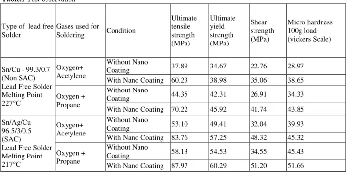
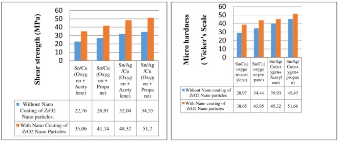
Thus the above four mechanical testing were done on different soldering parameters to check the feasibility of the Nano structured Coating application of ZrO2 Nano particles on Lead Free solders. The different parameters considered are Soldering done by the application of Oxygen + Acetylene flame, Soldering done by the application of Oxygen + Propane flame., Soldering done using Sn/Cu Solder with the Nano Structured coating application., Soldering done using Sn/Cu Solder without the Nano Structured coating application. Additionally the Nano structured
coating’s characteristic feature to improve the mechanical strength is also
confirmed and verified by applying all the above parameters in Sn/Ag/Cu solder at a composition of Sn96.5/Ag3/Cu0.5 with a melting point of 217°C.
Test Observations
Electronic waste management for sustainable growth
Table.1 Test observation
Type of lead free Solder
Gases used for
Soldering Condition
Ultimate tensile strength (MPa) Ultimate yield strength (MPa) Shear strength (MPa) Micro hardness 100g load (vickers Scale)
Sn/Cu - 99.3/0.7 (Non SAC) Lead Free Solder Melting Point 227°C
Oxygen+ Acetylene
Without Nano
Coating 37.89 34.67 22.76 28.97
With Nano Coating 60.23 38.98 35.06 38.65
Oxygen + Propane
Without Nano
Coating 44.35 42.31 26.91 34.33
With Nano Coating 70.22 45.92 41.74 43.85
Sn/Ag/Cu 96.5/3/0.5 (SAC)
Lead Free Solder Melting Point 217°C
Oxygen+ Acetylene
Without Nano
Coating 53.10 49.41 32.04 39.93
With Nano Coating 83.76 57.25 48.32 45.32
Oxygen + Propane
Without Nano
Coating 58.13 54.53 34.55 45.43
With Nano Coating 87.97 60.29 51.20 51.66
Thus, the results obtained for the soldered work pieces with nano coating were found to be comparatively increasing in all aspects as shown from Figure.3 to Figure.6.
Fig .3 Increase in Tensile Strength Fig .4 Increase in Yield Strength
Sn/Cu (Oxygen + Acetylene) Sn/Cu (Oxygen + Propane) Sn/Ag/Cu (Oxygen + Acetylene) Sn/Ag/Cu (Oxygen + Propane) Without Nano Coating of ZrO2
Nano particles 37,89 44,35 53,1 58,13 With Nano Coating of ZrO2 Nano
particles 60,23 70,22 83,76 87,97
0 10 20 30 40 50 60 70 80 90 100 0 10 20 30 40 50 60 70 Sn/Cu (Oxygen + Acetylen e) Sn/Cu (Oxygen + Propane) Sn/Ag/C u (Oxygen + Acetylen e) Sn/Ag/C u (Oxygen + Propane)
Without Nano Coating of
ZrO2 Nano particles 34,67 42,31 49,41 54,33
With Nano Coating of
ZrO2 Nano Particles 38,98 45,92 57,25 60,29
Fig .5 Increase in Shear Strength Fig.6 Increase in micro hardness
Thus, a total of 24 tests were taken to find the mechanical properties of the solder with and without the nanostructure coating. And it was observed that the solder properties were considerably increased after the coating. Thus, this nanostructure coating had a great impact over the solder strength and hardness property. Table.2 consolidates the test results.
Table.2 Test Results
Type of lead free Solder
Gases used for Soldering
Increase in ultimate tensile strength
%
Increase in ultimate yield strength
%
Increase in shear strength
%
Increase in micro hardness
%
Sn/Cu - 99.3/0.7 (Non SAC) Lead Free Solder Melting Point 227°C
Oxygen+
Acetylene 58.96% 12.43% 54.04% 33.41%
Oxygen +
Propane 58.33% 8.53% 55.10% 27.73%
Sn/Ag/Cu - 96.5/3/0.5
(SAC) Lead Free Solder
Melting Point 217°C
Oxygen+
Acetylene 57.74% 15.86% 50.80% 13.49%
Oxygen +
Propane 51.33% 10.56% 48.10% 13.71%
CONCLUSION
Thus with the addition of ZrO2 Nano particles over the Sn/Cu lead free solders
through such as tensile strength yield strength, micro hardness and shear strength increases at an average of 50 %. Because of this characteristic feature, the life of the solder joint is increased and it is confirmed that life increase is upto 50% of the original life. Considering the safe environment impact and high mechanical performance of the lead free solder due to Nano Structured Coatings of ZrO2 Nano
particles, Sn/Cu lead free solder can be widely preferred for usage in every electronic application like mobiles, laptops, computers etc. Due to the increased
en + Acety lene)
en + Propa ne)
en + Acety lene)
en + Propa ne) Without Nano
Coating of ZrO2 Nano particles.
22,76 26,91 32,04 34,55
With Nano Coating of
ZrO2 Nano Particles 35,06 41,74 48,32 51,2
Sh ylene) pane)
ene) e)
Without Nano coating of
ZrO2 Nano particles 28,97 34,44 39,93 45,43
With Nano coating of
Electronic waste management for sustainable growth
Coating is commercially successful.Nano Structured Coating of thickness 814 nm, it is evident that the mechanical properties
REFERNCES
1. Zhang, L. and K. Tu, Structure and properties of lead-free solders bearing micro and nano particles. Materials Science and Engineering: R: Reports, 2014. 82: p. 1-32.
2. Zhao, Z., et al., Effect of nano-Al 2 O 3 reinforcement on the microstructure and reliability of Sn–3.0 Ag–0.5 Cu solder joints. Microelectronics Reliability, 2016. 60: p. 126-134.
3. Chellvarajoo, S., M. Abdullah, and Z. Samsudin, Effects of Fe 2 NiO 4 nanoparticles addition into lead free Sn–3.0 Ag–0.5 Cu solder pastes on microstructure and mechanical properties after reflow soldering process. Materials & Design, 2015. 67: p. 197-208.
4. Chellvarajoo, S., M. Abdullah, and C. Khor, Effects of diamond nanoparticles reinforcement into lead-free Sn–3.0 Ag–0.5 Cu solder pastes on microstructure and mechanical properties after reflow soldering process. Materials & Design, 2015. 82: p. 206-215.
5. Chellvarajoo, S. and M. Abdullah, Microstructure and mechanical properties of Pb-free Sn–3.0 Ag–0.5 Cu solder pastes added with NiO nanoparticles after reflow soldering process. Materials & Design, 2016. 90: p. 499-507.
6. Sun, H., Y. Chan, and F. Wu, Effect of CNTs and Ni coated CNTs on the mechanical performance of Sn57. 6Bi0. 4Ag BGA solder joints. Materials Science and Engineering: A, 2016. 656: p. 249-255.
7. Xu, L., et al., Design and performance of Ag nanoparticle-modified graphene/SnAgCu lead-free solders. Materials Science and Engineering: A, 2016.