Tomás Rosa Calmeiro
Bachelor of Science in Biology
Atomic force microscopy assisted with
electron and ion beam microscopy for
the direct measurement of
biostructures and DNA samples
Dissertation to obtain a Master degree in Biotechnology
Supervisors: Tito Busani, Research Professor, University
of New Mexico
José Ricardo Ramos Franco Tavares,
Assistant Professor, Universidade Nova de
Lisboa
Jury:
President: Pedro Miguel Ribeiro Viana Baptista, Associate Professor
External Examiner: Peter Jonathan Eaton, Associate Researcher
II
Atomic force microscopy assisted with electron and ion beam microscopy for the direct measurement of biostructures and DNA samples
Copyright ©
Tomás Rosa Calmeiro, Faculdade de Ciências e Tecnologia, Universidade Nova de Lisboa
A Faculdade de Ciências e Tecnologia e a Universidade Nova de Lisboa têm o direito, perpétuo e sem limites geográficos, de arquivar e publicar esta dissertação através de exemplares
III
Resumo
Nesta dissertação apresenta-se estudos no campo da biotecnologia através de
microscopia de força atómica (AFM), uma técnica normalmente associada a ciências de
materiais. Apresenta-se, com especial destaque elementos de biologia molecular e
bionanotecnologia. Analisou-se ADN, insulina e enzimas de restrição como objectos isolados, a
fim de documentar propriedades como morfologia ou comportamento, e também no contexto
das interacções entre si. Analisou-se com especial atenção a interacção entre ADN e a
endonuclease EcoRV. O estudo de nanopartículas de ouro pretendeu estabelecer uma relação
entre a funcionalização desta e a medição do aumento do diâmetro médio por AFM. Dada a
natureza destes objectos de estudo, modificaram-se e avaliaram-se tanto protocolos de
imobilização como de preparação, considerando medições ao ar ou em líquido. Para alcançar o
objectivo de desenvolver medidas com maior sensibilidade e resolução aumentada,
modificaram-se pontas de AFM através de revestimentos metálicos e microscopia electrónica de
varrimento assistida com focagem de feixe de iões. Testes feitos com estas pontas confirmaram
o sucesso das modificações e que estas estavam funcionais, confirmando-se isto através da
aquisição de medidas e imagens mais sensíveis e de qualidade superior, quando comparadas
com pontas que não foram modificadas.
Palavras-chave: Microscopia de força atómica, AFM, bionanotecnologia, interacções
V
Abstract
Studies of atomic force microscopy (AFM), a technique commonly associated with
material sciences, in the field of biotechnology, with special emphasis on molecular biology and
bionanotechnology elements, are presented herein. DNA, insulin and restriction enzymes were
analysed as isolated objects, in order to document properties like morphology and behaviour,
and also on the interactions between each other. The interaction between DNA and the EcoRV
restriction endonuclease was especially highlighted. Gold nanoparticles were also studied in an
attempt to establish a relationship between functionalization and average diameter shifts, as
perceived by AFM. Given the nature of these objects of study, both immobilization and
preparation protocols were modified and evaluated, considering measurements in air or in
liquid. To serve the objective of developing probes with higher sensitivity and resolution,
especially for liquid measurements, AFM cantilevers were modified through metallic coatings
and scanning electron microscopy assisted with focused ion beam (SEM-FIB). Tests performed
with these probes confirmed that the modifications were successful, the probes are functional
and can aid in the production of better quality images, through the acquisition of sharper data in
comparison with non-modified probes.
Keywords: Atomic Force Microscopy, AFM, bionanotechnology, DNA-protein
VII
Table of contents
Resumo ... III
Abstract ... V
Acknowledgments ...XIX
Abbreviation list ...XXI
1. Motivation and objectives of this dissertation...1
1.1. Motivation for microscopy developments...1
1.2. Objective of the experimental work of this dissertation ...3
2. Nanotechnology in biological sciences: analytical tools ...5
2.1. Microscope types, basic physics of operation and limitations...5
2.2. Beyond visible light: Electron Microscopes ...6
2.3. The Scanning Electron Microscope and its potentialities...7
2.3.1. Focused ion beam ... 10
2.4. The first Scanning Probe Microscope ... 11
2.5. Atomic Force Microscopy: origins, instrumentation, basic principles of operation, advantages and disadvantages ... 12
2.5.1. Origins of the AFM ... 12
2.5.2. Instrumentation ... 12
2.5.2.1. Piezoelectric actuators... 13
2.5.2.2. Force transducers ... 14
2.5.2.3. Feedback control ... 14
2.5.2.4. Force Curves ... 15
2.5.3. Channels of acquisition ... 15
2.5.4. The probe ... 16
2.5.5. Artefacts ... 17
2.5.6. Main advantages over microscopy techniques ... 19
2.5.7. AFM Contact Mode ... 20
VIII
3. Atomic Force Microscopy applied to DNA, proteins DNA-protein and
nanoparticle-protein interactions ... 25
3.1. AFM in liquid media and force spectroscopy ... 25
3.2. Phase mapping versus topographic mapping: why is it so useful in biological sample imaging?... 28
3.3. AFM tip modifications and relation to resolution of an AFM ... 30
4. Modification of AFM probes ... 35
4.1. Focused ion beam milling to enhance lateral resolution ... 35
4.1.1. Contact mode tip modification with FIB SEM ... 35
4.1.2. Lateral resolution results and comparison ... 37
4.1.3. Gold-Palladium coating of tips and horizontal resolution comparison ... 39
4.1.4. Gold-palladium coating of AFM probe backside to enhance photodiode detection 40 5. AFM comparison studies – Insulin and gold nanoparticle conjugates ... 43
5.1. AFM measurement and analysis of amyloid insulin ... 43
5.1.1. Overview on insulin and rationale for selecting this hormone ... 43
5.1.2. Results of AFM measurements and analysis ... 44
5.1.3. Discussion and comparison between air and liquid acquisition ... 46
5.2. AFM measurements of uncoated and functionalized gold nanoparticles ... 47
5.2.1. Gold nanoparticles and their application to bionanotechnology ... 47
5.2.2. Development of AFM measurement protocol ... 48
5.2.3. Results of gold nanoparticle measurements: average height shifts ... 50
5.2.4. Discussion of gold nanoparticle results ... 52
6. AFM measurements of DNA ... 55
6.1. HRPII plasmid DNA... 55
6.2. DNA preparation for AFM measurements ... 55
6.3. Results of DNA measurements ... 56
IX
6.3.2. Morphology and dimensions of DNA: width vs. height, topography vs.
phase, high resolution imaging and plasmid sequence length prediction ... 59
6.4. Discussion of DNA results ... 61
6.5. Comparison between single (ssDNA) and double stranded DNA (dsDNA) imaging under AFM ... 64
6.5.1. Difference between ssDNA and dsDNA and preparation for AFM ... 64
6.5.2. Results and discussion of ssDNA imaging ... 65
6.6. Measurements of plasmid DNA undergoing EcoRV digestion ... 67
6.6.1. Overview on restriction enzymes, on EcoRV and objective ... 67
6.6.2. Preparation of the DNA-EcoRV measurement ... 68
6.6.3. Results of the DNA-EcoRV reaction ... 70
6.7. Discussion ... 75
7. Conclusions ... 77
8. Future prospects ... 81
9. References ... 83
I. Appendix ... i
a. Material and methods ... i
i. General information on equipment, operation and facilities ... i
ii. AFM probe index ... ii
iii. AFM probe modifications ... ii
iv. Insulin measurement conditions... ii
v. Material and methods of gold nanoparticle functionalization ... iii
XI
Index of equations
Equation 2.1 – Resolution of a system dependent from wavelength. ...5
Equation 2.2 - Equation for Hooke‟s Law ... 20
Equation 2.3 - Equations for amplitude and resonance frequency shifts ... 22
Equation 3.1 Simplified equation of Bustamante et al. for a simple spherical tip shape 32
Equation 3.2 Prediction of the width of a structure with a Rs radius when measured with
XIII
Index of Figures
Figure 2.1 – Basic schematic and components of operation of a SEM. ...8
Figure 2.2 - Schematic of the interactions between elements that give birth to secondary
electrons (SE), backscattered electrons (BSE) and emission of X-rays (X-ray) in SEM imaging.
Orange circles represent electrons while the grey circles the atom nucleus. ... 10
Figure 2.3 – Diagram of FIB milling of a surface (exemplified as an AFM probe) by
sputtering with a focused ion beam. The collision of the ion beam with the surface results in the
sputtering of surface atoms, together with beam atoms and secondary electrons. ... 11
Figure 2.4 – Simplistic schematic of an AFM‟s using an optical lever as force
transducer. ... 13
Figure 2.5 – Simplified force-distance curve for the interaction of an AFM probe and a
sample. ... 15
Figure 2.6 – Topographic (A), amplitude (B) and phase (C) images of the surface of a
human hair. ... 16
Figure 2.7 – Schematic of a chip with an AFM probe. The chip can be locked in the
AFM and the cantilever is left protruding, with the probe ready to interact with the sample. .... 16
Figure 2.8 – Tip related artefacts and their effects on image quality. Because images are
convolutions of tip geometry, when a tip fractures in unexpected manners, it can produce odd
features, such as spherical structures becoming triangular (A). Contaminations on the sample
can also be dragged by the tip, leading to images with both good quality and bad quality
sections alternated (B). If a tip picks up contaminants or breaks in two, resulting in two
structures touching the sample at the same time, this can lead to the appearance of multiple
images of the same feature (C) compared to an image clear of artefacts (D). ... 18
Figure 2.9 – Examples of drift. Both the spherical nanoparticles (A) and the spherical
liposomes (B) appear as elongated features. ... 19
Figure 3.1 – Thermal capture of an Olympus BC-AC40TS both in air and liquid. The
main resonant peak shifts from approximately 100 kHz to 25 kHz and a broadening in the peak
(lower Q factor) occurs. ... 27
Figure 3.2 – Force curve acquired by inward force spectroscopy on a protein, with detail
of the effect on cantilever bending at near setpoint zero (squared area). Setpoint zero refers to
the height from the sample at which the feedback control acknowledges the standard tip-sample
distance for imaging and switches the z-axis control on. In this case, its refers to the height in
which net attractive forces were first detected. ... 28
Figure 3.3 – Effect of changing different wave variables compared to the original wave
XIV
above them) and have similar parameters, except for amplitude, frequency and phase,
respectively. ... 29
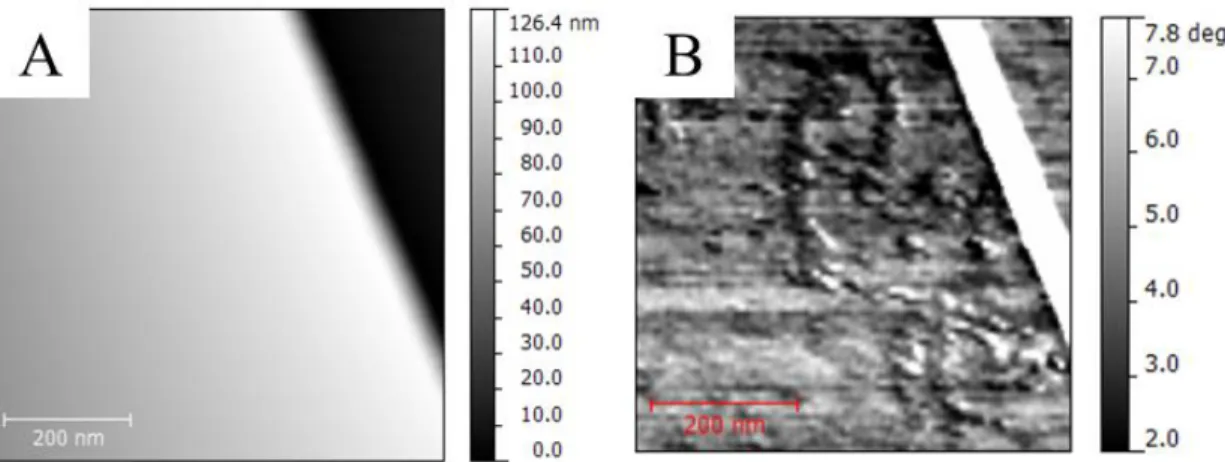
Figure 3.4 – Difference between topographic and phase imaging. The scale on the
topographic image (A) was selected using the automatic scaling given by the AFM software. It
can be seen that no DNA can be observed due to the existence of features several times larger
than its height, which mask it. However, using phase imaging (B) makes it possible to observe
subtle DNA molecules in the same area. ... 30
Figure 3.5 - Simulation of aliasing of the UNL logo. The first image is the original, the
second one averages the colour value of each 4 pixels into 1, the third one each 16 pixels into
one and the fourth each 64 pixels into one. ... 33
Figure 4.1 - Scanning electron microscope image of AFM probes after milling with the
focused ion beam. ... 36
Figure 4.2 – 3D rendering of the FIB generated comparison feature. ... 37
Figure 4.3 - Results of operation with FIB milled probe. Topographic image of the
comparison feature when done with an unmodified probe (A) and with the FIB milled probe (B)
and respective height profiles ... 38
Figure 4.4 –Elemental maps of the probe‟s tip by EDS. A: Elemental map of silicon. B:
Elemental map of gold. ... 39
Figure 4.5 - Images produced by unmodified and coated probes were done in the same
area of a silicon surface, marked with a red rectangle (A). Topographic images of this area done
with an unmodified probe (B) and with a coated probe (C), as well as amplitude imaging done
with an unmodified probe (D) and with a coated probe (E) are presented together with RMS
values. ... 40
Figure 4.6 - Comparison between topographic images of DNA molecules done with an
uncoated probe (A) and a probe with its backside coated (B)... 41
Figure 5.1 - A: Topographic image of amyloid insulin, both in aggregate and in fibril
form. B: stretched insulin fibrils. ... 44
Figure 5.2 – Topographic image and height profile example of the structural periodicity
observed in insulin fibrils acquired in air. ... 45
Figure 5.3 – Height profile of an insulin fibril measured in air. ... 45
Figure 5.4 – Comparison of box plots of insulin widths and heights measured in air and
in liquid media. ... 45
Figure 5.5 - Insulin fibrils measured in liquid. Red arrows mark the structural
periodicity. ... 46
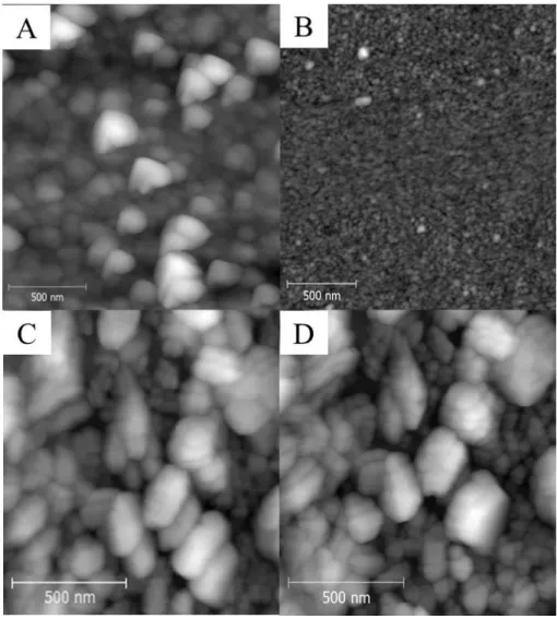
Figure 5.6 One of the many citrate crystals that grew from the deposited nanoparticle
solution (A). These masked the nanoparticles but in some situations it was possible to detect
XV
Figure 5.7 - Examples of topographic imaging of different batches of conjugates. ... 51
Figure 5.8 - Box plots of nanoconjugate diameter distributions as measured by the three
indicated methods... 52
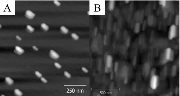
Figure 6.1 - Topographic image of DNA molecule acquired in liquid with Olympus
TR800PB probe... 57
Figure 6.2 - Topographic image of several HRPII plasmids (A) and detail of one of
these molecules where the circular configuration can be seen (B). ... 58
Figure 6.3 - Schematic on the reason why DNA, being a cylindrical molecule, appears
with different values when acquired on the z axis (height) and on the x0y plane (width) due to
convolution effects. ... 58
Figure 6.4 - A clear difference in the sharpness of the DNA boundaries can be seen
when comparing between topographic acquisition (left image) and phase acquisition (right
image). ... 59
Figure 6.5 - Topography of a DNA molecule where a pattern repetition can be observed.
... 60
Figure 6.6 – Box-plot of the distance between crests measured on the DNA molecule. 61
Figure 6.7 – Images of a DNA molecule with the areas selected for pitch distance
studies marked. These were used to produce the height profiles and the box-plot graph. ... 61
Figure 6.8 – Average width values measured for the different probes used in the
experiment in nanometres. „Average res.‟ refers to AC160TS probes, „High res. unmod‟ to the
unmodified SSS-NCH and „High res. mod‟ to the gold-palladium coated SSS-NCH.
Topography and phase refers to the channels in which the measurements were obtained. ... 64
Figure 6.9 - Topographic images of aggregated ssDNA molecules as a result of DNA
melting and intra and inter-strand homology. In A, a detail of the condensed structure can be
seen while in B several DNA aggregates can be observed. ... 65
Figure 6.10 Phase imaging of ssDNA condensing around contaminants. These appeared
both as long and thin objects with boundaries in white (A) and globular objects (B, pointed by
arrows). ... 66
Figure 6.11 Topographic images of DNA plasmids and EcoRV units, marked as white
arrows. As can be seen by the lower magnification (A) and higher magnification image (B),
EcoRV units appear as bright dots which can be both associated with DNA or unbound on the
substrate. ... 70
Figure 6.12 EcoRV units seem to have rough surfaces, both when measured in the
topographic channel (A) and in the phase channel (B). Background was removed to aid in the
XVI
Figure 6.14 – Phase image (A) and diagram (B) of the DNA-EcoRV conjugate. The red
arrow in the phase image marks the zone where DNA was cleaved and the white one the
location of the EcoRV unit. ... 72
Figure 6.13 Topographic (A) and phase (B) imaging of an EcoRV aggregate resting
against the substrate. ... 72
Figure 6.15 – Examples of possible DNA-EcoRV cleavage complexes. The squared
area in images A and B shows the areas which generated images C and D. Bend angle
measurements were done in these, as represented by the yellow lines in images G, H, I and J.
Images. E and F represent schematics of these complexes. ... 74
Figure I.1 – Microscope equipment used in this dissertation‟s experiments: the AFM
Asylum Research MFP-3D Stand Alone(A) and the dual beam SEM-FIB Zeiss Airuga (B). ... i
Figure I.2 – Transmission electron microscope image of the gold nanoparticles before
XVII
Index of tables
Table 5.1 - Means and standard deviations of nanoparticle conjugate diameters as
calculated by the indicated methods and difference between mean values obtained for
AuNP-MUA and AuNP-AuNP-MUA-BSA conjugates. All values are in nanometres. ... 51
Table I.1 – Specifications of AFM probes used in this dissertation as advertised by
XIX
Acknowledgments
To Tito Busani for taking me as his student, for teaching me the basics of AFM
operation and instrumentation, for answering all the questions, for standing by me when I
needed, for reviewing the dissertation, especially the parts related to physics, and overall for
being a friend with whom many hours were spent in the laboratory.
To Ricardo Franco for taking me as his student, for planning the biotechnological
component of the dissertation together with me and Tito, and for sharing his remarkable
know-how in bionanotechnology. I am also thankful for the exhaustive reviewing and corrections of
the dissertation, especially in the biological oriented experiments.
To Joana Vaz Pinto for selflessly finding the time and availability to review some
chapters of this dissertation, pointing some mistakes, making some suggestions and answering
and explaining some more advanced doubts in Physics. Thank you for the time working
together and for sharing your invaluable knowledge with a permanent smile on your lips.
To Inês Gomes, João Luz and Tiago Monteiro, from Bionano@requimte, for the good
times in their company and for their aid in the nanoparticle functionalization and DNA isolation.
To Ann-Katrinn Awizio and Friedhelm Freiss from AtomicForce F&E GmbH (Asylum
Research) for the outstanding and joyful support, for taking the time to teach me liquid mode
operation, force spectroscopy and advanced AFM modes, as well as answering all the weird
questions of an AFM initiate without laughing.
To Pedro Viana Baptista for allowing me to extract DNA in his laboratory (Centro de
Investigação em Genética Molecular Humana, FCT-UNL). My thanks also go to Pedro Pedrosa
and Bruno Viegas for guiding me throughout the original DNA extraction protocol whenever I
needed.
To Elvira Fortunato, for allowing me unrestricted access to the facilities of
CENIMAT/I3N, especially to the atomic force microscope. I also wish to thank the rest of the
CENIMAT/I3N crew for their warm welcoming and for receiving me as one of them.
To Sara, because actions speak louder than words.
To Family, for always being there, it doesn‟t matter if I did or didn‟t need it. Thanks for
the blind support throughout all these years and for making me who I am (deal with it!). Thanks
to Simão, for randomly waking up at 4 am and, upon realizing I am awake, happily strolling to
XXI
Abbreviation list
AC – Alternate Contact
AFM – Atomic Force Microscope/Microscopy
AuNP(s) – Gold Nanoparticle(s)
BSA – Bovine Serum Albumin
BSE – Backscattered Electrons
DNA – Deoxyribonucleic Acid (ds – double stranded; ss – single stranded)
EDS – Energy Dispersive X-Ray Spectrometry
FIB – Focused Ion Beam
MEMS – Microelectromechanical systems
MUA – Mercaptoundecanoic Acid
PDB – Protein Data Bank
SE – Secondary Electrons
SEM – Scanning Electron Microscope/Microscopy
SPM – Scanning Probe Microscope/Microscopy
STM – Scanning Tunnelling Microscope/Microscopy
1
1.
Motivation and objectives of this dissertation
1.1.
Motivation for microscopy developments
In some science fields, such as pure mathematics, advances in knowledge and new
findings can depend uniquely on the development of new theories and hypothesis. This
particularity arises from their abstract nature or near independence of equipment. However, this
is not true for all fields of study. Biology, especially some of its subdisciplines like
microbiology or molecular biology, are flagrant cases of fields of study that have always been
highly dependent of advances in other fields.
Only after some phenomena were discovered and some devices invented, it was
possible for biologists to develop their own new methods and protocols to study their targets of
interest. It‟s almost like saying that, in some situations, we must first wait for physicists, mathematicians or chemists to study, propose and develop novel methods of study and analysis
before biologists have the proper tools to prove or disprove their own theories.
On another hand, curiosity is a defining attribute of the human species. Apart from
biological reasons (such as the development of human intelligence derived from the evolution of
the brain), it is the fundamental attribute responsible for the technological development
achieved by humanity throughout its period of existence. The wish of seeing and understanding
both unseen phenomena and objects, be it what lies far away in the night sky or what makes up
everyday objects, are possibly among the oldest desires of mankind. To fulfil this wish, many
devices and methods throughout history were proposed and used, allowing studying what the
eye cannot see.
This desire of seeing what is so small the eye cannot discern has been present
throughout the entire history of biology, and is linked to one of its defining inventions: the
microscope. This milestone invention was fundamental in several findings such as the
discoveries of unicellular organisms by van Leeuwenhoek in the 17th century, or that cells
divided to originate new ones during mitosis, by researchers such as Remak, Kölliker or
Flemming in the 19th century.
There are some examples that, in some circumstances, biologists may have to wait
before their proposed theories can finally be visually or analytically confirmed. For example,
although some had already hypothesized the existence of organisms small enough to be seen
with the naked eye, centuries would have to pass before visual, unequivocal evidence of the
existence of bacteria could be presented with the invention of the microscope. A more recent but
similar example that also shows the dependence from advances in other areas is the discovery of
2
pathogen too small to be seen with an optical microscope and several scientists backed this
assertion throughout decades through indirect methods, since existing optical microscopes
didn‟t allow seeing more than very small undetailed bodies. Only in 1931, with the invention of the electron microscope, microbiologists had the tools to finally obtain visual confirmation of
the existence of virus and to study their structure and morphology, allowing their cataloguing
and establishing connections with so many diseases1–4.
The objective of this dissertation and, by extension, the laboratory worked developed
with it, was beyond acquiring the skills needed for atomic force microscopy operation and
preparation, especially oriented at biological fields. The great objective of studies that gather
several areas of study is to bring together - as has been done by others with great success and
benefits to research and industry - the knowledge and know-how of two very distinct areas of
study. Although investigation of “pure disciplines” must be respected and fomented, it is also
undeniable that many advances in science arise from interface studies where the best of what
each field has to offer can be gathered. This way, it becomes possible to merge the potentialities
of more than one area, what has the possibility of improving the approaches to phenomena and
our understanding of them, as well as the amount of methods to study them. For that reason,
nanoscale phenomena and devices are some of the objects of study in which most of the
attention rests on, due to their novelty and ground breaking implications for future generations
and technology5.
Over the next decades, nanotechnology and the areas which emerged out of it, such as
bionanotechnology, will surely grow to occupy a place in society far greater than what it
occupies today, what arises from its potential of explaining and exploring phenomena that up to
now are not perfectly understood or, while being, couldn‟t yet be integrated into devices that
have everything to become ground breaking inventions. These possibilities lead some to defend
that nanotechnology has the potential of ultimately transforming society in a way similar to the
discovery of maritime trade routes or the industrial revolution6.
It is also undeniable that, as has happened and still happens with most developments in
biotechnology in general, bionanotechnology is a relatively young area of study full of potential
but also experimentations that delve deep into new phenomena or into the manipulation of
structures at nanometric scale, triggering novel phenomena. Many of these have not been
thoroughly studied, meriting great attention and care with the possible future implications that
the manipulation of these elements may hold, not only for humanity as for the entire biosphere.
Several entities already underline the importance of supervision and regulation of
3
Knowing this, it becomes of the utmost importance that there is equipment able to
document and analyse how nanodevices and their constituents operate, how they influence the
media surrounding them and also how classic elements of other areas, ranging from metal wires
to nucleic acids, behave when conjugated with these novel structures as far as on the atomic
level. This is why there is interest in the development of protocols and methods that allow
pushing the boundaries of the existing technology and aid in the understanding of phenomena
that may possibly be the core of the operation of futuristic devices.
1.2.
Objective of the experimental work of this dissertation
The overall objective of this dissertation rests, first of all, in the interest in the
continuous development of methods and techniques that allow visualizing and understanding
biological phenomena, both from a more morphological and classic point of view, such as cell
imaging, down to more state of the art applications, such as single molecule interactions.
Therefore, two main components - one more technical and another more research oriented, in
which biological studies took place - are approached in this dissertation.
The technical component basically included learning how to operate the AFM,
understanding its components, learning how to critically analyse images, especially on the
differences between the types of information acquired, to grasp the concepts that explain
differences in modes of operation and how resolution is affected by the AFM‟s elements. AFM
on itself is not a very hard or demanding technique so it is relatively straightforward to learn the
basics required to start producing simple, low magnification images, and to move to more
challenging samples by building upon experience over time.
This training initially comprised learning basic modes of operation, such as standard
alternate contact modes or contact mode in air. The aim was to move to more challenging
modes, such as liquid mode operation or force spectroscopy, and even becoming familiar with
methods and modes of operation that are less AFM biology oriented, which are often demanded
in characterization jobs or projects.
The research oriented part, although far more biological oriented, also had experiments
related with physical modifications of the AFM probe as means to improve resolution.
Understanding and using common protocols of immobilization for the biomolecules studied
throughout this dissertation‟s experiments, as well studying the dimension, structure and
morphology of these biostructures, both when isolated and when reacting with one another were
also considered key objectives. Liquid mode operation was also to be approached and the
4
Insulin, DNA and the enzyme EcoRV were used, with each of these biostructures being
analysed individually. However, due to the specificity and knowledge of the interaction between
DNA and EcoRV enzymes, the dynamic interaction between these two was also focused in an
attempt to establish the possibility of observing the cleavage mechanism with AFM.
Gold nanoparticles functionalized with different coatings, such as in the absence or
presence of a BSA protein coating, were also studied as model for the use of gold nanoparticles
functionalized with other elements, such as antibodies for diagnosis or treatment.
On the subject of probe modifications, two main objectives were approached in this
dissertation: tip modification by focused ion beam and tip coating with nanometric metallic
layers to protect tips from oxidation or enhance resolution.
The focused ion beam approach can be used to modify tips up to the scale of its
resolution, which can routinely be as small as one nanometre. The modifications that were
planned were projected for operation at larger scales than those used in most of the biological
studies to be presented herein. However, these are intended to serve as clear indications of the
positive effect that these modifications can have on measurements as well as how the
development of this technique can lead to the fabrication of sharper and more sensitive tips,
without needing expensive and less replicable functionalizations such as with carbon nanotubes.
The determination of the use of coatings as a factor affecting the quality of the measurement,
both positively and negatively, will also be approached.
Through all of this, it is desired that this dissertation serves as a document that
reinforces the use of AFM as a, if not the, primary technique for high resolution imaging of
biological structures, especially with the potential of characterizing interactions between them in
5
2.
Nanotechnology in biological sciences: analytical tools
2.1.
Microscope types, basic physics of operation and limitations
As of today, there are several types of microscopes operating in everyday research and
industrial environments, from which three are more commonly used - the optical microscope,
the electron microscope and the scanning probe microscope – although each of these spawn
several subtypes of their own. Each one of these has its advantages and limitations, inherent to
the way they are operated and the way they interact with the sample. For example, the optical
microscope operates using light and can be as simple as a child‟s toy, while electron
microscopes are expensive and complex, using electron beams instead of sunlight or light bulbs,
and requiring controlled environments. The other main microscope type is the scanning probe
microscope, in which sample interaction is undertaken by a sharp tip contacting or interacting at
a nanometric distance with a sample‟s surface.
The operating limit of optical, and even of electron microscopes, is normally associated
with the wavelength of the element that interacts with the sample, as happens in the case of the
classical optical microscope. In most of the nowadays optical microscopes, a beam of white
light is focused by optical lenses and transmitted through the sample. Due to different
absorption behaviour of different materials before incident light, a contrasting image between
transparent media and opaque or highly refractive media is produced. More complex
microscopes, such as the scanning near-field optical microscope, have been developed, showing
that the resolution limits dictated by visible light could be surpassed by using apertures smaller
than the wavelength and acquiring the reflected light at such a close distance from the surface
that it does not travel the necessary length to diffract. However, the fact is that the key of this
design is the existence of a hollow needle collecting the light very close to the surface and not
the cascade of magnifying lens popularly associated with a regular microscope8,9.
The resolution limit of these images is not only determined by the wavelength, but also
by the numerical aperture of the focusing lenses and observation media. Images acquired
through this technique will start losing quality below resolutions of 400 nm, since that is the
wavelength of violet light, while images below roughly 200 nm of resolution will be of bad
quality, as determined by the Abbe diffraction limit equation, shown below10.
Equation 2.1 – Resolution of a system dependent from wavelength.
In the equation, d is the minimum resolution possible to attain, i.e., the smallest distance
6
the beam of the incident wave, n is the refractive index of the observation medium and θ the
diffraction angle of the lens. The calculation of “nsinθ” defines the value of the numerical
aperture (NA)11. It can be, therefore, inferred from the equation that there are two ways of
improving resolution knowing that there is a limit to diffraction angles: operating in media with
higher refractive indexes, in order to increase numerical aperture, or using beams of smaller
wavelengths, like ultraviolet light waves of other nature, like the mentioned electron waves10,12.
This second method is precisely the one which was applied to electron microscopes in order to
go beyond the resolution attained by visible light. In this type of microscopy, the traditional
beam of visible light used in optical microscopes, with nanometric wavelengths, is replaced by
an electron beam with a wavelength orders of magnitude below that, effectively pushing the
resolution limit to values that can go as far as the ångstrom (100 pm) and the magnification to
values in the range of the millionth13.
2.2.
Beyond visible light: Electron Microscopes
The most well-known electron microscopes are the scanning electron microscope
(SEM) and the transmission electron microscope (TEM). The basics behind the operation of
both microscopes are the same: an electron beam undergoing electromagnetic focusing is aimed
at a sample, being the main difference the way through which detection of the sample occurs.
In a TEM, basically, the beam is transmitted through a thin slice of the sample, where
elastic and inelastic scattering of electrons occur. These are then propagated through imaging
lenses and into a detector opposed to the electron source14. On the other hand, detection on a
SEM is not so straightforward: when the electron beam is accelerated towards the sample, the
atoms on its surface will have their original electrons substituted by those in the beam or just be
plainly deflected away from the sample, what will allow for different sample characteristics to
be inferred and shown, after these electrons have been captured by detectors with different
properties8,15.
However, both these microscopes have disadvantages of their own. For example, to
produce quality images, they must be operated in vacuum or else the electron beam will be
dispersed by the particles naturally present in the atmosphere, meaning the amount of electrons
and the energy they carry, when interacting with the sample, will be deficient to produce any
image15,16.
Another important disadvantage is that, under normal conditions of operation, it is
impossible, or very challenging, to image insulating materials, since they tend to capture the
electrons, instead of conducting them away to the ground of the stage. When this happens, the
7
electric shield, deflecting incident electrons on their own, leading to the observation of erratic
features in the images.
Other disadvantage related to the incident electron beam is that this beam carries a high
amount of energy with it. Therefore, many soft and organic materials can be damaged by the
energy released from the interaction of radiation with matter. The result is usually an increase in
the local temperature. Biological samples, from tree leaves to proteins or DNA in a buffer
solution (which carries the issue of making an observation difficult or impossible in vacuum)
are usually clearly damaged by those effects. It is possible to overcome some of these problems
by coating the materials with a metallic, and therefore conducting, nanometric layer. However,
when the purpose is observing, documenting and studying phenomena at nanometric scale, a
layer of 10 nm of any coating material may mask, or even destroy, details that one wants to
observe10,15,17–19.
These limitations are some of the reasons why these microscopy techniques were out of
bounds in many situations to biological and biomedical research, and as will be presented
below, one of the reasons why scanning probe microscopy techniques, became such an
interesting approach to research on biological samples.
2.3.
The Scanning Electron Microscope and its potentialities
The first microscope using electrons as element of sample interaction was developed in
1931 by Max Knoll. Knoll‟s microscope proved that, although with worse magnification than a
standard optical microscope, electrons could be used to obtain magnified images of samples,
giving birth to the field of electron microscopy. However, the first microscope equipment worth
of being qualified as a scanning electron microscope (SEM) was only developed by Mandred
von Ardenne in 1937. This SEM was the first electron operated microscope to obtain high
resolution by focusing an electron beam onto a surface and producing a raster image without
chromatic aberrations20. Chromatic aberrations spoiled images in both optical and electron
microscopes because lenses don‟t exhibit the same refractive indexes for all wavelengths,
meaning a focused, unique wavelength element had to be used or else images produced would
become blurry after a set magnification, like can be seen in the edges of items in deficiently
focused photographs21. The resolution of the SEM respects the Abbe diffraction limit, meaning
that in theory it can achieve 2 pm of resolution. However, other significant factors contribute in
limiting the magnification of this microscope, such as beam diameter, interaction volume or
signal-to-noise ratios, leading to real resolution values closer to 1 nm in average recent
8
When producing an image, the most common mode of sample interrogation is done by
detecting the electrons ejected away from the outer shells of the atoms constituting the surface
of the material under observation. These electrons are called secondary electrons, which lends
name to this main mode of operation, offering resolutions up to half nanometre in the most
powerful equipment. The other most known imaging mode is the backscattered electrons mode,
which can also give insight on the different chemical compositions of surfaces8.
As it has been just mentioned, the scanning electron microscope produces images at the
cost of focusing electrons, which are accelerated with a given voltage away from a source. By
extrapolating the position and behaviour of these electrons, it becomes possible to map
topography or chemical differences through the use of detectors present in the sample chamber.
In most SEMs, the electron source, called the electron gun, relies on a tungsten or
possibly lanthanum hexaboride filament, which is heated up until it becomes thermionically
activated: when temperature is high enough to favour the emission of electrons. There is another
type of electron emission, which relies on field emission, in which a needle emits electrons by
setting a voltage bias near the electron source with an extractor, leading to electron extraction by
quantum tunnelling. These sources must be monochromatic, i.e., to emit an element of a single
wavelength, in order to avoid the mentioned aberrations. These electrons are then
electromagnetically focused in the electron column by a set of condenser lens, generating a
beam as sharp as possible, since a thin and energetic beam is a requirement for high
magnification imaging. The focused beam is then deflected by deflection coils mounted just
before the opening to sample chamber, which allows for the beam to be aimed along the surface
of the sample in order to produce a raster scanned image. The detectors lie inside the sample
9
chamber, strategically placed to favour the detection of the different types of electrons that are
produced by the sample; or even electromagnetic radiation like X-rays. Secondary electrons are
produced by inelastic scattering of the electron beam, i. e., an electron which was ejected due to
a collision with an incident electron in which there is no conservation of energy. These electrons
are called low energy electrons because there is loss of kinetic energy related to collisions
occurring when the electron travels through the atoms on its way to the surface. These ejected
electrons normally originate from the k-shell of the atoms and must be attracted by electrical
bias to the respective detector, because, although they carry enough energy to be ejected and
cross some atoms, they cannot go further than few nanometres from the surface. After detection
of electrons and steps of electrical amplification, it is possible to extrapolate their position and
intensity of the signal in order to produce a contrasting image. This image depends on the
amount of secondary electrons being emitted, allowing for a topographic image of the sample to
be produced15,20,24. Figure 2.1 represents the basic instrumentation of a SEM.
On the other hand, backscattered electrons are produced by elastic scattering of the
electrons. This mode of operation allows building a relative map of the elements on the sample
surface, since higher atomic number atoms favour the generation of more backscattered
electrons. The equipment used to detect this type of atoms does not need to make use of electric
bias because, while secondary electrons originate from the sample and carry less energy,
backscattered electrons originate from the electron beam and therefore have higher energy,
being deflected back (hence backscattered) by the atoms and exiting the sample with enough
strength to collide with the detector. The amount of backscattered or deflected electrons rise in
proportion to the atomic number of an element‟s atoms because such elements have more
massive nucleus, which deflect more electrons in comparison to lighter elements. This data will
offer topographic data with less resolution; however it will be far more informative if the
objective is to determine that there are different elements present in the sample surface. This
type of information is also very interesting because it can be used in electron backscattering
diffraction (EBSD), a technique in which backscattered electrons are diffracted following a
pattern directly related to the crystalline orientation of the material under observation, allowing
mapping and identifying the crystal system of a sample15,25.
Other types of techniques that were of interest to this dissertation and which were used
are energy-dispersive X-ray spectroscopy (EDS) and focused ion beam (FIB).
Energy-dispersive X-ray spectroscopy is a technique that allows the analysis of the elements
constituting a sample and to produce an element map of the different chemical elements that
compose it. It is based on the principle that when an electron beam interacts with the atoms on
the surface of the sample, there is a chance that an electron orbiting the inner electron shells of a
10
occupied by a higher energy electron orbiting in the outer electron shell, which will lose the
excess energy when moving to the inner shell through the emission of an X-ray photon. The
energy carried by this photon is specific for the atom and for the shell the electron originates
from and, therefore, with the appropriate detector, it is possible to measure the number and
energy of X-ray emissions and to determine with high precision what elements constitute the
sample and where they are located15.
2.3.1.
Focused ion beam
The technique of focused ion beam (FIB) is discussed together with the SEM because,
although this is not an electron microscope since the sample interacting element are ions, the
fact is that they are similar pieces of equipment, in which sample interrogation and detection is
based on the same principles. Many SEMs incorporate FIB columns in their machinery,
constituting two-beam systems and allowing, besides standard SEM imaging, to collect other
data or to nanofabricate structures by depositing new atoms, or sputtering original ones away
from a surface8,15,26.
This technique relies on the use of a liquefied gallium source covering a tungsten tip.
Through the use of a field emission extractor, an electric field capable of ionizing gallium is
generated. These ions can then be accelerated towards a sample with nanometric precision, what
can have different outcomes intimately related with the desired application27. These can be used
for micro and nanofabrication, which can follow both a top-down and a bottom-up approach.
For the former, its destructive properties can be used to mill and sharpen features or create
precise patterns by removing the atoms of a material off a surface, such as when sharpening an
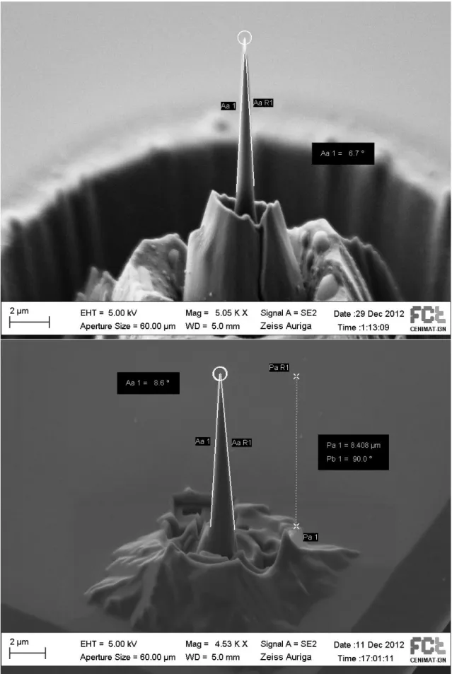
AFM probe in order to enhance its resolution (Figure 2.3), an interesting possibility approached
in this dissertation. For the latter, its constructive properties can be used in order to deposit
atoms on the surface and fabricate structures. By injecting a precursor gas to form a film
containing the element we are interested in depositing, the FIB beam can be used to dissociate
and breakdown this film, forming thin, precise deposits that can be used in the fine construction
11
of microcircuits, for example. FIB systems can also be used to modify the surface, such as by
implanting beam atoms in it or be used for surface interrogation and analysis, because of the
emission of secondary electrons as in SEM and also for surface characterization, such as in
grain size measurements, since ions are channelled in different directions in relation to the grain
sizes of the material and the angle of incidence, allowing the generation of 3D images
micrometres into the material27–29.
2.4.
The first Scanning Probe Microscope
The invention of the scanning tunnelling microscope (STM) in 1981 by Gerd Binnig
and Heinrich Rohrer at IBM Zürich, gave birth to a new type of microscope that didn‟t fit into
the already existing categories of optical microscopy or electron microscopy. This microscope
was dubbed the first type of scanning probe microscope ever created, becoming a breakthrough
in the field of microscopy for a variety of reasons related to, for example, the way it interacted
with the sample associated with the magnifications and resolutions it allowed to attain.
The fundamental characteristic that defines scanning probe microscopy is that the
images of a sample are generated by the interaction between it and a probe (a needle or a sharp
tip), instead of with electromagnetic waves. For the first time, the limit of a microscope was not
defined by phenomena like diffraction of light, the length of the wave used in its operation or
lens apertures, but by how sharp a probing item can be and the sensitivity of the feedback circuit
that monitors its movement.
Scanning probe microscopy spawned many different microscopy techniques, but the
two most widely used and known are two: scanning tunnelling microscopy (STM) and atomic
force microscopy (AFM). In scanning tunnelling microscopes, which can routinely achieve true
atomic resolution, surface detection is done by closely approaching a conducting tip to a surface
in which both are under a chosen electric current and voltage: the difference of the applied
voltage between both is known. When the distance between the tip and sample is extremely
small, i. e., roughly half nanometre, the voltage bias is enough to allow electrons to tunnel
12
through the gap between the two by quantum tunnelling. Knowing this, it is possible to map the
surface of a sample by crossing the detected changes in electric current over the voltage applied
and the position of the tip over time30,31.
2.5.
Atomic Force Microscopy: origins, instrumentation, basic principles
of operation, advantages and disadvantages
2.5.1.
Origins of the AFM
The first device that can be tracked as the ancestor of the atomic force microscope is the
stylus profilometer, invented in 1921 by Schmalz. This “microscope” obtained information on a
surface by dragging a probe, like a cantilever with a sharp tip, along a sample surface in a raster
fashion. This allowed to obtain several profile lines that when merged together would make a
projection of the topography of a surface. This was achieved by setting a cantilever probe on a
fixed position with its tip touching the surface and then using a stage to move the sample
horizontally. These cantilevers would bend and twist as they encountered the features of the
moving surface and by using a light beam aimed at a mirror on the cantilever, it was possible to
record the changes in cantilever position using photographic paper, since height shifts would
change the mirror position and divert the beam to different locations. However, the forces
applied to the cantilever meant that it could bend or crash against large features, leading to
cantilever damage, diminishing resolution, or damaging the sample. One proposed solution for
such issues was to oscillate the cantilever above the sample, lowering the forces involved in the
probe-sample contact while still keeping surface tracking possible, a proposal that was
ultimately introduced in AFM31,32.
2.5.2.
Instrumentation
It can be said that an atomic force microscope is almost like a very sensitive and
fine-tuned profilometer because both stand on the same principle of dragging a tip on a surface to
measure it. However, while profilometers only measure the difference in height when the probe
is in contact, the AFM measures the interaction forces between the sample and the tip, besides
the possibility of detecting several properties due to a far more complex instrumentation.
The fundamental concepts involved in its instrumentation are three: piezoelectric
transducers, force transducers and feedback control. Piezoelectric materials have the property of
changing their dimensions when an electric potential is applied to them and vice versa, with
typical sensitivity going as low as ångstromic changes per volt. The inclusion of these elements
in the stage (xy plane) and the cantilever holder (z axis) allows to control with astonishing
precision the movement of the sample below the probe, as well as how high this probe needs to
be to interact with the surface satisfactorily. This vertical interaction can be detected by force
13
must have sensitivity beyond 1 nN, allowing registering the intensity of the force between a
probe and a sample.
The last fundamental element is feedback control, which monitors and registers such
force values and feeds commands to the piezoelectric actuators in order for them to dilate or
compress and keep the tip interaction force at a pre-set value. Simply put, when the sample
moves under the probe and a feature appears that would bend the cantilever up or down, the
force transducer will detect a sudden raise or decrease of force and redirect this information to
the actuators, so that the z axis actuator can move the tip away, before it crashes the surface, or
bring it closer so it can keep on tracking at the same distance and same net force (Figure 2.4)32–
34
. While this, it can also generate reference signals which can be compared with the received
signals and used to generate images.
2.5.2.1.
Piezoelectric actuators
The precision scan of a sample is only possible because of the use of piezoelectric elements
throughout the three axis of operation of the AFM. Different voltage values can be fed to these
elements in order to generate precise movements, not only to move the sample in regards to the
probe, the x-y plane, but also on the z axis, fundamental to maintain the probe-sample
interaction at a fixed value. This can be achieved by using piezoelectric ceramics such as
amorphous lead barium titanate (PbBaTiO3) or lead zirconate titanate (Pb[ZrxTi1-x]O3 with
0<x<1), which can be formulated to have smaller coefficients of expansion but higher linearity
and vice versa, hence the respective definitions of hard and soft ceramics. These elements can
limit how fast an AFM can operate because the rate at which they can do contraction and
extension cycles defines how quick the sample can be scanned. It is desired that these exhibit
14
linearity between applied voltage and dimension changes at all times and in all conditions,
however, this is not always true as discussed in the Artefacts section below33.
2.5.2.2.
Force transducers
Force transducers are the elements responsible for detecting shifts in the force exerted
on the probe‟s tip. Although it is deducible that they must be extremely sensible in order to detect variations smaller than the nanometre in the z axis, their precision is also required so that
force differences can be detected long before they become enough to damage a tip, especially in
modes of operation in which the probe enters repulsive regime. In this case, very small variation
in tip-sample distance will generate large force differences, due to the steepness of the force
curve in the repulsive regime, as will be explained in the „Force curves‟ section below.
Originally, cantilever deflection was detected relying on STM electronics and an STM
probe. However, AFMs using this method, along with others such as relying on interferometers
or piezoelectric principles, are a minority compared to those relying on the principle of the
optical lever, due to the high sensitivity of this method associated to its simplistic design as well
as the ease and cost advantage of producing AFM probes with reflective coats. The only
downsides are that these coatings may lead to non-reproducibility and the alignment, if manual,
may be time consuming and, if done incorrectly, may give rise to image artefacts33,35,36.
The optical lever works on the principle that the reflective back of a probe can reflect a
laser beam from an emitter to the centre of a photodiode. This photodiode has, for example, four
quadrants, which will produce voltage proportional to the amount of light that they receive.
When the probe is deflected or twists, the beam will move away from the centre and into one of
the quadrants, generating an electric potential that, when detected, can be used to deduce
information from the surface such as height or lateral deflection similar to the photographic
paper of the profilometer37.
2.5.2.3.
Feedback control
The reason why an AFM scan can attain such magnifications is also related to a fine
feedback system which can almost instantly collect the information obtained by the force
sensors, process it, and generate signals to control the elements fundamental to the scan, such as
piezoelectric actuators. At the same time as this data is processed to generate an appropriate
response to changes in topography, the difference between the inputted and the outputted
signals throughout the various channels can be registered. These signals include and are not
limited to, for example, z voltage and error signal, amplitude and phase in the case the cantilever
15
etc… The difference in these signals can then be translated by appropriate software and form maps of the surface of the sample.
2.5.2.4.
Force Curves
The force between the probe and the surface plays a defining role in atomic force
microscopy and is intimately related with certain types of operation. When the distance between
a probe and the surface starts to decrease, at first a cantilever just stays in its relaxed position.
However, as the cantilever distance starts to shrink to values on the range of the few hundreds of
nanometres, attractive forces (van der Waals or capillary effects, for example) start to play a
considerable role and the probe will be snapped in the direction of the surface. However, as the
distance keeps decreasing, net repulsive forces (for example, from the convergence of electron
clouds) will start to dominate this interaction and the tip will be bent back away from the sample
with increasing strength in relation to how small the gap becomes (Figure 2.5). This principle is
transversal to all AFM modes of operation and is exploited in several modes of imaging, while
also explaining certain outcomes of operating in certain modes (like why probes are more prone
to damage in contact mode operation)38.
2.5.3.
Channels of acquisition
When operating an AFM, it is common for it to output more than just one type of signal,
such as topography. For example, in contact mode, while the topographic image of the surface
is generated using the z piezoactuator voltage signal, the AFM can also collect its error signal
(how much it was being deflected before the feedback circuit corrected the height) or the lateral
deflection of the cantilever (how the interaction with the surface made it bend laterally). In
oscillating modes, the same thing can be done, allowing to visualize topography as well as, for
example, alterations in the frequency, amplitude or phase of the cantilever oscillation, as
represented in Figure 2.6. This allows obtaining several readings of the sample at the same time.
16
2.5.4.
The probe
Although every single circuit or element present in the AFM is important for it to
deliver what is demanded of it, there is not a more fundamental element to create a good
measurement than the AFM probe. The probe is of the utmost importance for an AFM
measurement because, in most cases, it will be its properties determining the quality of a
measurement, since it is the element responsible of collecting the information in situ. There are
no perfect probes and even excellent probes will produce some artefacts, which are presented in
the section below (2.5.5), in certain conditions39. However, probes from the same fabricant are
expected to be homogeneous and to operate under the same conditions, being expected of them
to behave in a precise and replicable way, allowing an experienced operator or any experienced
person who analyses the images to read beyond these artefacts.
For ease of manipulation, because probes are disposable and are easily replaced, these
Figure 2.6 – Topographic (A), amplitude (B) and phase (C) images of the surface of a human hair.
17
are sold on standardized substrate chips. These chips have the cantilevers, which carry the
probe, protruding from one of its sides (Figure 2.7). Probes are fabricated relying on MEMS
technologies and there are two main groups of probes: silicon nitride probes, more flexible and
often with a triangular shape and a square pyramidal probe and also silicon probes, stiffer and
usually rectangular, with triangular pyramidal or conical probes. Contact mode oriented probes
usually have low (on the range of the few dozen kilohertz) resonant frequencies, spring
constants below 1 N/m and are fabricated from silicon or silicon nitride (Si3N4). Alternate
contact probes are stiffer, with spring constants which can be of several dozen newton per
meter, and have higher resonant frequencies, which in the most recently developed biology
oriented can be as high as 1.5 MHz, although general purpose probes are commonly oscillated
in values between 70 and 400 kHz. They are normally only fabricated out of silicon32,33,40.
Probes are normally modified with coatings to increase the voltage generated by the
photodiode and, therefore, the sensitivity of the measurement. However, these can be
extensively modified, as will be focused with more detail on Chapter 3.3. The probes used in
this dissertation‟s experiments and their main characteristics can be seen in Table I.1 of
Appendix I.a.ii.
2.5.5.
Artefacts
An artefact is a feature that appears during a scan which is not real. While in some
situations these may be obvious to the operator, in other situations they can be subtle and
mislead, requiring some experience to detect them. West and Starostina consider that there are
four primary sources of artefacts: the probe, the scanner elements, the image processing and
external vibrations, although other also exist41.
Probe related artefacts originate from the fact that images generated by AFM are
convolutions of the tip geometry and the features of the sample. This can lead to different
situations like small protruding structures appearing larger than they are in reality, while holes
in the surface will appear smaller in width and depth because the tip cannot penetrate in it.
Alterations in probe geometry due to bluntness, tip contamination or cracking of the tip,
forming a double tip can also introduce several unreal features on the images (Figure 2.8).
Scanner elements can also affect the quality of acquisition because piezoelectric
elements are not infallible when it comes to the precision of its movement. Phenomena like
thermal drift, hysteresis or creep are vulgarly associated with AFM and can degrade image
quality (Figure 2.9). Thermal drift is related to the heating of the equipment during operation,
affecting the linearity of piezoelectric expansion and contraction due to changes in the
environmental conditions for which parameters were initially tuned. Hysteresis and creep are
18
follow the same behaviour pattern when doing symmetric movements, what can be due to
inherent characteristics, such as the age or operation hours of a system or acquired due to
outside factors, like temperature. Hysteresis relates to the principle that any piezoelectric
element tends to maintain the state it is in, in a principle that can be compared to inertia. This
means that the voltage needed to generate a specific change in dimension, may not be enough to
produce the same change in other situations or, on the other hand, may be excessive. Creep is a
similar phenomenon that derives from the fact that when a sudden change in voltage is applied
to a piezoelectric actuator, the response behaviour may not be totally linear: there can exist a
lagging period before it exhibits motion or, in the opposite case, there can exist situations that
after the voltage input has been interrupted, the element keeps on behaving as if it was still
under the effect of that input, although this is rare in the most common closed-loop operation
(with XY correction engaged)42.