Brazilian Journal of Physics, vol. 36, no. 2A, June, 2006 317
Characterization of CdTe Thin Films Grown on
Glass by Hot Wall Epitaxy
Sukarno Olavo Ferreira∗, F´abio Fagundes Leal∗, Tatiana Estorani de Faria∗, Jos´e Eduardo de Oliveira∗, Paulo Motisuke†, and Eduardo Abramof†
∗Departamento de F´ısica, Universidade Federal de Vic¸osa, 36570-000 Vic¸osa-MG, Brazil and
†Laborat´orio Associado de Sensores e Materiais, Instituto Nacional de Pesquisas Espaciais,
Caixa Postal 515, 12245-970 S˜ao Jos´e dos Campos-SP, Brazil
Received on 4 April, 2005
In this work we have investigated the properties of CdTe thin films grown on glass substrates by Hot Wall Epitaxy. Its most important feature is the growth at very low temperatures, which would allow the growth even on polymer substrates. Our samples were grown at temperatures between 150 and 250oC at a growth rate
between 0.2 and 2 µm/h. The CdTe films were characterized by x-ray diffraction, scanning electron microscopy and optical transmission. The x-ray teta-2teta scans revealed films with cubic structure and a very high degree of preferential orientation. In fact, for films thicker than 1 µm, no other reflections have been observed on the spectra besides the (111), (333) and (444). The scanning electron micrographs showed a grain size about 0.3
µm and the optical transmission indicated a very good optical quality of the interfaces, showing pronounced
interference fringes.
Keywords: Thin films grown; Hot wall epitaxy; CdTe
The production of CdTe thin films has been investigated for many years. The semiconductor properties of this material are suitable for application in solar cells and many other opto-electronic devices such as detectors for the infrared and x-ray [1-4].
The most used techniques to obtain these films are organo-metalic chemical vapour deposition [5], closed spaced subli-mation [6], physical vapour deposition [7], molecular beam epitaxy [8], electrodeposition [9] and sputtering [10]. All these techniques have advantages and disadvantages depend-ing on the type of application intended for the film. Parame-ters such as range of deposition temperatures and growth rates obtained, type of substrates used and films produced (epitaxial or polycrystalline) must all be of concern.
In this work we describe the production and characteriza-tion of CdTe thin films grown on glass substrates. The growth technique used was the Hot Wall Epitaxy (HWE) and the films were characterized by scanning electron micrographs, atomic force microscopy (AFM), x-ray diffraction and optical trans-mission in the visible and near infrared.
I. EXPERIMENTAL
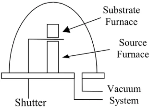
The HWE growth system used is shown in Fig. 1. It consists of a two furnace system, for source and substrate, separated by a shutter. The deposition occurs at pressures between 10−6 and 10−7Torr, obtained by a diffusion pump.
High purity commercial CdTe (99.999%) was used as source material and the source temperature can be controlled from 400 to 590oC. In this temperature range CdTe evapo-rates congruently with more than 98% of CdTe molecules in the vapor. The growth rates obtained were in the range be-tween 0.01 and 10 ˚A/s. In this work we have used growth rates between 0.5 and 5.5 ˚A/s.
The HWE is a well established technique able to produce
Substrate
Furnace
Source
Furnace
Vacuum
System
Shutter
FIG. 1: HWE growth system.
very high quality epitaxial films on many crystalline substrates like Silicon, Gallium Arsenide, Barium Fluoride and others [11-13]. However, there is no report on its use with amor-phous substrates. We have used common microscope glass, 0.5 mm thick as substrate. The 9 x 9 mm samples were de-greased with acetone, truly washed in deionized water and gently etched for 2 minutes in a 2% HF solution. In the growth system the substrates were pre-heated to 350oC prior to growth. The growth temperatures used were between 150 and 300oC. Such a low growth temperature is one of the ad-vantages of this growth technique since it makes possible the use of pre-processed substrates, a very important feature for some applications, [14] and the fabrication of hybrid devices using polymer substrates. [15]
318 Sukarno Olavo Ferreira et al.
the investigated range. The thickness was obtained averaging at least eight measurements around the sample perimeter. The thickness uniformity was better than 5% for all samples.
FIG. 2: Thickness as a function of growth time for three different source temperatures. The solid lines are just guides to the eyes.
Scanning electron micrograph reveals a grain size which varies slowly from about 0.2 µm for thinner samples to about 0.5 µm for the thicker samples. Fig. 3 shows a scanning elec-tron micrograph of a 1.5 µm thick sample taken at 15 kV with a 20000 magnification. One can clearly see that grain size distribution is very uniform.
FIG. 3: Scanning electron micrograph of a 1.5 µm thick sample.
Detail investigation of sample morphology was made using a Digital Multimode atomic force microscope, operating in tapping mode. Fig. 4 shows a 2 µm x 2 µm AFM image of a 2.5 µm thick sample. The image clearly reveals that the grains have a pyramidal shape. This would be expected for films with preferential growth in the [111] direction, since CdTe has the zincblende structure.
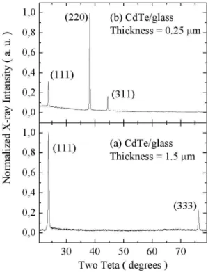
To confirm this point, the structural properties of the grown layers have been investigated by x-ray diffraction using a Philips X’Pert diffractometer. The teta-2teta scans, obtained in the Bragg-Brentano geometry, have revealed that all grown films with thickness above about 1 µm, exhibited only the (111), (333) and (444) diffraction peaks, indicating highly tex-tured samples with a preferred [111] growth orientation. In
FIG. 4: AFM image of a 2.5 µm thick sample. Image size is 2 µm x 2 µm.
the range investigated, neither the substrate temperature nor the growth rate has shown any influence in the film texture, which could be measured just by these teta-2teta scans.
The only factor that affects film texture is the sample thick-ness. This fact can be seen in Fig. 5, where we show the dif-fraction spectra for two samples grown with the same parame-ters (growth rate and substrate temperature), but with different thickness. The diffraction pattern in Fig. 5a, obtained for a 1.5 mm layer, shows only the (111) and (333) peaks. Even in a logarithmic scale is not possible to distinguish other peaks. In Fig. 5b, for a 0.25 µm film, the intensity of the (220) peak is even higher than that of the (111) and one can also observe the (311) reflection.
Brazilian Journal of Physics, vol. 36, no. 2A, June, 2006 319
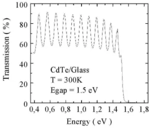
FIG. 6: Transmission spectra of 2.57 µm thick CdTe layer.
This result indicates that the growth process initiates by the nucleation of islands with all possible orientations, but as the growth proceeds the [111] direction dominates, and after the deposition of about 1µm almost all grains have this orien-tation. This preferential [111] orientation has already been observed for other growth techniques almost independent of substrate material, but in most cases it happens only for high substrate temperatures, usually above 500oC. [16] The pro-duction of highly oriented films at such low temperature is a great advantage of the HWE technique, which has not been reported before.
We have also investigated the optical quality of the grown layers using transmission in the visible and near-infrared
re-gion. As one can see in Fig. 6, the transmission shows clearly interference peaks indicating the high quality of both film in-terfaces. The gap energy determined from this data is 1.528 eV, which coincides with the value reported in the literature for bulk CdTe at 300 K. Assuming that the index of refraction is equal to 2.75, one can use the interference fringes to cal-culate the film thickness to compare with the values obtained using the perfilometer. The values agree within 10%.
II. CONCLUSION
CdTe polycrystalline thin films were grown using the Hot Wall epitaxy technique on glass substrates. All samples pro-duced are highly textured, with preferential orientation in the [111] direction. The degree of orientation increases with layer thickness and for samples thicker than 1 µm no other diffrac-tion peak is observed besides the{111}family. Pronounced interference fringes in the transmission spectra indicate a very good optical quality. The most important result is the fact that such high quality and oriented layers were obtained at a very low growth temperature of 150oC. Such a low process-ing temperature has not been reported before and opens the possibility for the growth on pre-processed substrates already containing electronic circuits and also on polymer substrates.
Acknowledgement
We would like to thank Dr. N. Speziali and A. Melo for the help with x-ray diffraction measurements. This work has been supported by CAPES, CNPq and FINEp brasilian agencies.
[1] T. Aramoto, S. Kumazawa, H. Higuchi, T. Arita, S. Shibutani, T. Nishio, J. Nakagima, A. Hanafusa, T. Hibino, K. Okamura, and M. Murozomo, Jpn. J. Appl. Phys. 36, 6304 (1997) [2] P. V. Meyers, S. P. Albright, Prog. Photovolt.: Res. Appl.8, 161
(2000).
[3] J. Rams, N. V. Sochinskii, V. Munoz, and J. M. Cabrera, Appl. Phys. A, 71, 277 (2000).
[4] A. M. D. Ede, E. J. Morton, and P. de Antonis, Nucl. Instrum. Methods, A458, 7 (2001).
[5] I. Mora-Ser´o, C. Polop, C. Ocal, M. Aguil ´o, and Mu˜noz-SanJos´e, J. Crystal Growth 275, 60 (2003).
[6] T. Okamoto, A. Yamada, and M. Konagai, J. Crystal Growth
214/215, 1148 (2000).
[7] G. G. Rusu, M. Rusu, Solid State Comunications 116, 263 (2000).
[8] L. A. Almeida, L. Hirsch, M. Martinka, P. R. Boyd, and J. H. Dinan, J. Electronic Materials 30, 608 (2001).
[9] H. Gomez, R. Henriquez, R. Schrebler, R. Cordova, D. Ramirez, G. Riveros, and E. A. Dalchiele, Electrochimica Acta
50, 1299 (2005).
[10] A. Gupta, A. D. Compaan, Appl. Phys. Lett. 85, 684 (2004). [11] S. Seto, S. Yamada, and K. Suzuki, Journal of Crystal Growth
214/215, 5 (2000).
[12] Georgi M. Lalev, Jifeng Wang, Seishi Abe, Katashi Masumoto, and Minoru Isshiki, J. Crystal Growth 256, 20 (2003). [13] S. O. Ferreira, E. C. Paiva, G. N. Fontes, and B. R. A. Neves, J.
Appl. Phys. 93, 1195 (2003).
[14] C. Schreiber, G. Giakos, Nucl. Instrum. Methods A458, 12 (2001).
[15] X. Mathew, J. P. Enriquez, A. Romeu, and A. N. Tiwari, Solar Energy 77, 831 (2004).