*e-mail: [email protected]
1. Introduction
With the increasing requirements on power eficiency and environment protection, rare-earth free permanent magnets with high energy product are urgently demanded for future technological advances on power transmission and utilization. The iron nitride ilm is one of these most attractive magnet systems. In the iron nitride family, there are various phases with different lattice structures and nitrogen concentrations. Among them, the α’’–Fe
16N2, γ’-Fe4N andε-Fe3N exhibit excellent magnetic properties1-3. Therefore, a lot of works have been focused on the formation of these desirable iron nitride phases. Many growth method, such as reactive magnetron sputtering, molecular beam epitaxy, nitrogen ion implantation and etc. have been applied on different substrate to grow iron nitride ilms which are mainly composed of α’’–Fe
16N2, γ’–Fe4N orε-Fe3N
[4-6]. The phase evolution of the iron nitride ilms
induced by thermal treatment was also studied. It was found that the α’’–Fe
16N2 phase is stable below 673 K and a slightly heated substrate will beneit the formation of α’’–Fe
16N2 [7,8]. Since
the nitrogen is one of the key points to manipulate the phase compositions in the iron nitride ilms, the effect of nitrogen content are extensively studied9,10. However, there are few reports on the effect of bias voltage. When sputtering is used as the deposition method, bias voltage plays an important role on the composition, structure and properties of the ilms and coatings. For instance, the surface grain size of the Ni ilms on a lexible substrate increases with the increase of the bias voltage11. When a proper negative bias was applied on the sample surface, the CrSiN coatings exhibit three-dimensional nanocomposite microstructure with superhigh hardness12,13.
In this work, we report the fabrication of iron nitride ilms with good soft-magnetic properties by changing the depositing bias voltage from +25 V to –50 V. When a positive bias voltage is used, we intend to heat the sample surface slightly by the collision electrons which are attracted by the positive voltage. When a negative bias is used, we try to form denser structure. The relationship among the bias voltage,
phase compositions and structure of the iron nitride ilms is investigated and discussed.
2. Material and Methods
2.1. Film deposition
The iron nitride ilms were deposited by radio frequency (RF) reactive magnetron sputtering in a mixture of Ar and N2 gases at a constant low ratio of 30.00:0.81. A Fe target (99.95%) with a diameter of 80 mm was used to provide Fe to the iron nitride ilms. During depositing, the working pressure was kept at 1 Pa. The bias voltage varied from +25 V, 0 V to –50 V and the corresponding as-obtained ilms are named as ilm 1#, 2# and 3#, respectively. (111) Si wafers was used as the deposition substrate.
The film thickness was measured by step profiler (DEKTAK 150). The chemical and phase compositions of the as-obtained iron nitride ilms were characterized by energy dispersive spectroscopy analyzer (EDS, FEI. Sirion 200) and X-ray diffraction (XRD) using Cu Kα radiation, respectively. Scanning electron microscopy (SEM, FEI Sirion 200) observation was performed on the iron nitride ilms to investigate the surface morphologies. The more detailed microstructure of the iron nitride ilms was studied by using transmission electron microscopy (TEM, FEI, Tecnai G2). The hysteresis loop of the ilms was recorded by a vibrating sample magnetometer (VSM, Lakeshore 7404) at room temperature. Before the measurements, the VSM was calibrated by a standard Ni sample.
3. Results
3.1. Formation of the iron nitride ilms at various
bias voltages
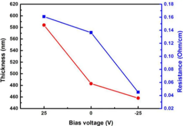
The thickness of the ilms as a function of the bias voltage is shown in Figure 1. Film 1# has a thickness of about 584 nm. The decrease of the bias leads to a decreasing ilm thickness,
Effects of Bias Voltage on Fen Films Prepared by Magnetron Sputtering
Yuqiao Zenga, Zheng Tana, Lichu Zhoua, Meiya Jianga, Yuedong Qiua, Feng Fanga, Haibo Huanga,
Xuhai Zhanga*, Jianqing Jianga
aJiangsu Key Laboratory of Advanced Metallic Materials, School of Materials Science and Engineering, Southeast University, Nanjing 211189, China
Received: September 30, 2014; Revised: September 30, 2015
Iron nitride ilms were deposited by radio frequency (RF) reactive magnetron sputtering at different bias voltages. It was found that the composition, structure and magnetic properties of the iron nitride ilms were strongly dependent on the depositing bias voltage. With a bias voltage of –50 V, the iron nitride ilm is fully dense and has a homogenous microstructure consisting of α-Fe and Fe16N2, leading to a unique combination of high Ms of 1645 emu/cc, Hc of 5 Oe and μI of 1573.
i.e. 483 nm at 0 V and 458 nm at –50 V. The most likely cause for the reduced ilm thickness is the decrease of macro defects such as voids or cracks. Usually the positive bias causes more macro defect sites in the functional materials and results in a loose structure. The negative bias can attract more positive ions to bombard the sample surface, leaving behind a dense structure. The electric resistance further proves the different number of macro defects of the iron nitride ilms deposited at different bias voltages. As shown in Figure 1, the electric resistivity of the ilm 1#, 2# and 3# is 0.161 ohm/cm, 0.137 ohm/cm, and 0.045 ohm/cm, respectively.
The chemical compositions of the iron nitride ilms are measured by EDS and the results are shown in Table 1. All the as-deposited samples contain both Fe and N elements, demonstrating the successful formation of iron nitride ilms in the depositing bias ranging from +25 to –50 V. The Fe/N ratio in the ilms keeps constant at about 12-13 as the bias voltage decreases from +25 V to 0 V. The further decrease of the bias to –50 V leads to the distinct increase of the Fe/N ratio (about 16). Usually, when sputtering is adopted as the depositing method, more negative bias leads to more
reacted N content in the ilms, since the negative bias will absorb more positive N ions to take part into the reaction with Fe. The similar phenomenon can be observed in TiN, CrN ilms and etc.14,15. However, when the positive bias voltage is used, a loose structure with a large number of voids and cracks will form. These macro defects can absorb the gas around themselves during the deposition. Therefore the EDS tests involved some unreacted N elements which exist as the absorbed N2 in the iron nitride ilms. When the bias voltage decreases, a denser structure with less macro defects can be obtained, where the amount of absorbed N2 will decrease and lead to a lower N content.
As is shown in Figure 2a, ilm 1# exhibits a rough surface which contains coarse pyrometric cones with a size of 30-50 nm, indicating the formation of a loose structure. The cone nature is always related to the surface diffusion process. The positive bias can attract a large number of negative electrons to the sample surface and thus enhance the local temperature on the surface. The increase of the temperature will cause higher surface diffusion rate and lead to the formation of coarse cones. Film 2# has a similar surface morphology (Figure 2b) as ilm 1#. When the depositing bias decreases to a negative value, a dense structure without any cone nature is formed in the ilm (Figure 2c), agreeing with the results of electric resistivity.
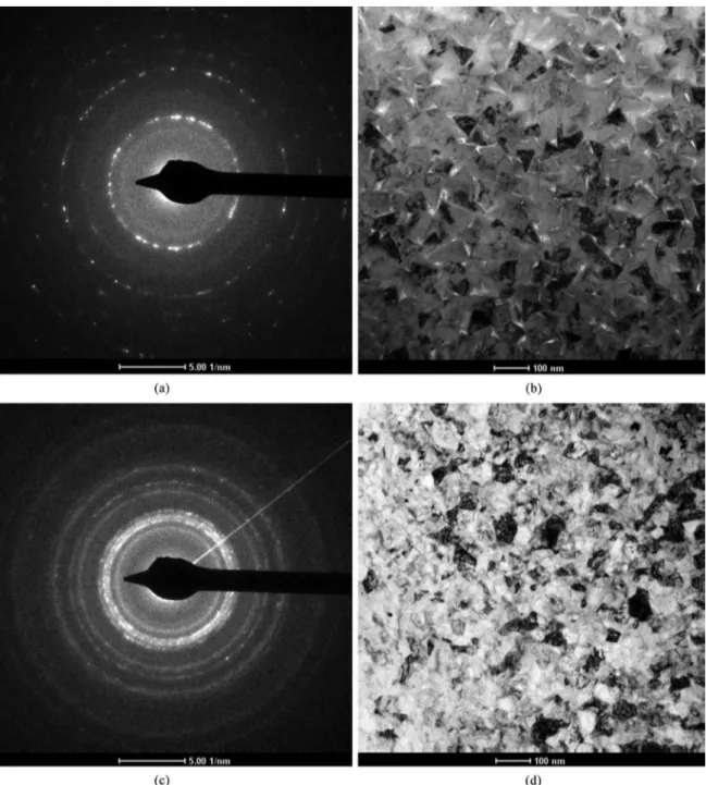
Films 1# and 2# have a similar microstructure. In the SEAD pattern of ilm 2# (Figure 3a) has strong signals of the (110), (200), and (211) planes of α-Fe. Meantime, a faint diffraction ring of the α’’–Fe
16N2 (112) can be identiied.
Figure 1. Thickness and the electric resistivity of the iron nitride ilms.
Table 1. Chemical compositions of the iron nitride ilms (measured
by EDS).
Films Fe content
(at.%) N (at.%) Fe/N
1# 92.3 7.7 12
2# 92.7 7.3 13
3# 94.2 5.8 16
This demonstrates the dominant growth of α-Fe and the coexistence of a small amount of α’’–Fe
16N2 on the Si substrate. The bright-ield TEM image in Figure 3b reveals that the cone shaped crystals in ilm 2# have sizes in the range of 50-150 nm. In the case of ilm 3#, the (110), (200), and (211) planes of α-Fe, together with the (112), (202) and (400) planes of α’’–Fe
16N2 can be identiied in the SEAD patterns in Figute 3c. The much stronger diffraction signals of the α’’–Fe
16N2 than that in Figure 3a suggests that the negative bias enhances the formation of α’’–Fe
16N2 in the iron nitride ilms. The bright-ield TEM image in Figure 3d shows that ilm 3# contains a homogenous crystalline
structure. The crystalline size in the direction parallel to the ilm surface is about 50-100 nm. The smaller crystal size in ilm 3# than that in ilm 1# and 2# can be explained by the improved formation of the α’’–Fe
16N2 in the ilm. The increasing amount of α’’–Fe
16N2 can provide the α-Fe more inhomogeneous nucleation sites and retards the growth of the α-Fe by making the atomic diffusion more dificult. As a consequence, the microstructure is reined.
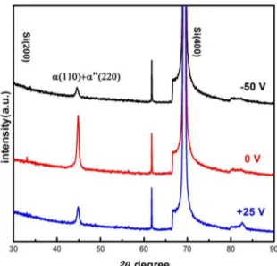
The phase evolution of the iron nitride ilms as a function of the deposition bias is also followed by XRD in Figure 4. Film 1#, 2# and 3# exhibit only one sharp peak at 2θ of about 44.58 degree, which is corresponding to the (110) of
α-Fe and (220) of α’’–Fe
16N2. In another words, the α-Fe and α’’–Fe
16N2 display a preferred growth behavior according to the (110) and (220) direction, respectively. Using the Scherer formula and the proile itting, the crystal sizes of both α-Fe and α’’–Fe
16N2 are estimated and summarized in Table 2. With the decreasing bias voltage, the α’’-Fe
16N2 is gradually reined. The α-Fe, on the contrary, gets coarsened. The results are in disagreement with the TEM observation in the plane view. However, it should be noticed that the crystal size derived from XRD data is according to the direction vertical to the sample surface. At this direction, the growth of the crystals is in a competitive way rather than though diffusion. The crystalline plane will display the higher growth rate if it contains lower chemical potential. For instance, when the N content increases, the (220) plane of TiN shows lower chemical potential than the (111) plane. The TiN will change the preferred growth direction from (111) to (200) when the N content is high enough16. In this study, the (111) plan of the α-Fe may exhibit lower chemical potential than the (220) plane of the α’’–Fe
16N2 when the bias voltages decreases from +25 V to –50 V. Thus the α-Fe will get the champion in the growth rate competition. As a result, in the direction vertical to the sample surface, the winner has larger crystal size and the crystal structure of the loser is reined.
3.2. Magnetic properties of the as-deposited iron
nitride ilms
The hysteresis loops of the iron nitride ilms prepared at different bias voltage is shown in Figure 5. All the iron nitride ilms exhibit a good magnetic softness. The detailed magnetic parameters, including HC, Ms and μI, are summarized in Table 3. In the case of HC, the decreasing bias from +25 V to –50 V leads to a dramatic decrease of HC from 91 Oe to 5 Oe. On the other hand, the MS and μI values increase with the decrease of the bias voltage and reach their maxim value (1645 emu/cc and 1572, respectively) at –50 V. Thus, the iron nitride ilm deposited at the negative bias voltage of 50 V exhibit the unique combination of lowest HC, highest MS and μI among the iron nitride samples deposited at different bias.
The possible origins of the good magnetic properties may come from three aspects. The irst lies in the macrostructure of the iron nitride ilms. The existence of macro void or cracks can be excluded by the negative bias voltage. Secondly, the crystal size matching is another important factor. The crystal size of ilm 3# in the direction parallel to the ilm surface is reined. It has been reported that the smaller crystal size in the iron nitride ilms is always associated with lower HC. In the direction vertical to the ilm surface, ilm 3# contains larger α-Fe than the other ilms. Larger crystal size can beneit the MS by reduce the spin disorder. Thirdly, it has been well documented that the phase composition is a key point to the magnetic properties. Since α’’–Fe
16N2 exhibit much higher MS than α-Fe, the higher α’’–Fe
16N2 content in the iron nitride ilms will result in higher MS.
4. Conclusions
A series of iron nitride ilms were deposited by RF reactive magnetron sputtering at various bias voltages. It was found that the composition, structure and magnetic properties of the iron nitride ilms were strongly depended on the depositing bias voltage. The bias of –50 V led to a unique combination of high MS of 1645 emu/cc, HC of 5 Oe and μI of 1573. A homogenous dense microstrure composed
of α-Fe and α’’–Fe
16N2 might be attributed to the high soft magnetic performance of the iron nitride ilm prepared at –50 V.
Figure 5. Hysteresis loop of the iron nitride ilms.
Figure 4. XRD patterns of the iron nitride ilms.
Table 2. Average grain size of α-Fe and α’’–Fe
16N2 calculated using
the Scherer formula.
Films α-Fe (nm) α’’–Fe
16N2 (nm)
1# 18 46
2# 31 19
3# >100 17
Table 3. Magnetic parameters of the iron nitride ilms.
Films MS (emu/cc) HC (Oe) μI
1# 1250 91 31
2# 1451 58 53
Acknowledgements
This work is supported by the Fundamental Research Funds for the Central Universities, National Science Foundation of China (51141004, 51201033), Specialized Research Fund for the Doctoral Program of Higher
Education (20110092120035), Opening Project of Jiangsu Key Laboratory of Advanced Metallic Materials (AMM201101), Opening Project of Jiangsu Key Laboratory of Material Tribology (kjsmcx1003), and Fundamental Research Funds for the Central Universities (3212003101, 3212002205, 3212003102).
References
1. Kim TK and Takahasi M. New magnetic material having ultrahigh magnetic moment. Applied Physics Letters. 1972; 20(12):492-494. http://dx.doi.org/10.1063/1.1654030.
2. Takahashi T, Takahashi N and Nakamura T. Preparation of freestanding Fe2N crystal by vapor-phase epitaxy under
atmospheric pressure. Materials Chemistry and Physics. 2004; 83(1):7-9. http://dx.doi.org/10.1016/j.matchemphys.2003.08.028.
3. Chen GM, Jaggi NK, Butt JB, Yeh EB and Schwartz LH.
Mossbauer and magnetic studies of ε-FexN, 2<x≤3. Journal
of Physical Chemistry. 1983; 87(26):536-5332. http://dx.doi.
org/10.1021/j150644a005.
4. Feng XP, Mi WB and Bai HL. Investigation of structure and magnetic properties of the as-deposited and post annealed iron nitride films by reactive facing-target sputtering. Applied Surface
Science. 2011; 257(16):7320-7325. http://dx.doi.org/10.1016/j.
apsusc.2011.03.112.
5. Sugita Y, Mitsuoka K, Komuro M, Hoshiya H, Kozono Y and Hanazono M. Giant magnetic moment and other magnetic properties of epitaxially grown Fe16N2 single-crystal films.
Journal of Applied Physics. 1991; 70(10):5977-5982. http://
dx.doi.org/10.1063/1.350067.
6. Jiang YF, Al Mehedi M, Fu EG, Wang YQ and Wang JP. FeN foils by nitrogen ion-implantation. Journal of Applied Physics. 2014; 115(17):17A753.
7. Terada N, Hoshi Y, Naoe M and Yamanaka S. Synthesis of iron-nitride films by means of ion beam deposition. IEEE
Transactions on Magnetics. 1984; 20(5):1451-1453. http://
dx.doi.org/10.1109/TMAG.1984.1063545.
8. Nakajima K, Yamashita T, Takata M and Okamoto S. Mobbauer study on Fe16N2 films prepped by ion-implant nitrification of
iron films. Journal of Applied Physics. 1991; 70(10):6033-6035. http://dx.doi.org/10.1063/1.350084.
9. Morisako A, Takahashi K, Matsumoto M and Naoe M. Iron nitride thin-films prepared by facing targets sputtering. Journal
of Applied Physics. 1988; 63(8):3230-3232. http://dx.doi.
org/10.1063/1.340851.
10. Mi WB, Feng XP and Bai HL. Magnetic properties and Hall effect of reactive sputtered iron nitride nanocrystalline films. Journal
of Magnetism and Magnetic Materials. 2011;
323(14):1909-1913. http://dx.doi.org/10.1016/j.jmmm.2011.02.043.
11. Koda T and Toyota H. Effects of magnetic flux density and substrate bias voltage on Ni films prepared on a flexible substrate material using unbalanced magnetron sputtering assisted by inductively coupled plasma. Journal of Vaccum Science &
Technology A. 2014; 32(2):02B104.
12. Wang QM and Kim K. Microstructural control of Cr–Si–N films by a hybrid arc ion plating and magnetron sputtering process. Acta Materialia. 2009; 57(17):4974-4987. http:// dx.doi.org/10.1016/j.actamat.2009.07.001.
13. Lin J, Wang B, Ou Y, Sproul W, Dahan I and Moore J. Structure and properties of CrSiN nanocomposite coatings deposited by hybrid modulated pulsed power and pulsed dc magnetron sputtering. Surface and Coatings Technology. 2013; 216:251-258. http://dx.doi.org/10.1016/j.surfcoat.2012.11.053.
14. Kong Q, Ji L, Li H, Liu X, Wang Y, Chen J, et al. Influence of substrate bias voltage on the microstructure and residual stress of CrN films deposited by medium frequency magnetron sputtering. Materials Science and Engineering B - Advanced
Functional Solid-State Materials. 2011; 176(11):850-854.
15. Wang Z, Zhang D, Ke P, Liu X and Wang A. Influence of substrate negative bias on structure and properties of TiN coatings prepared by hybrid HIPIMS method. Journal of
Materials Science and Technology. 2015; 31(1):37-42. http://
dx.doi.org/10.1016/j.jmst.2014.06.002.