Corresponding Author: Diana Marcela Narvaez Devia
10.1590/S1517-707620150001.0013
Received on: 21/10/2013 Accepted on: 04/09/2014
Bias voltage influence on the mechanical
and tribological properties of titanium
aluminum nitride coatings produced
by triode magnetron sputtering
Diana Marcela Devia Narvaez 1, Juan Manuel Velez Restrepo2 Elisabeth Restrepo Parra 3
1
Universidad Tecnológica de Pereira, Pereira, Colombia e-mail: [email protected],
2
Universidad Nacional de Colombia Sede Medellín, Laboratorio de Materiales e-mail: [email protected]
3
Universidad Nacional de Colombia Sede Manizales, PCM Computational Applications e-mail: [email protected]
ABSTRACT
TixAl1-xN coatings were grown using the triode magnetron sputtering technique with various bias voltages between -40 V and -150 V. As the bias voltage increased, an increase in the Al atomic percentage was obser-ved, presenting a competition with Ti and producing structural changes. Moreover, the grain size and rough-ness were also strongly influenced by the bias voltage. It was observed that coatings with concentrations of approximately 25% Al and 75% Ti exhibited an optimum mixture of mechanical and tribological properties.
The average coefficient of friction was low for the TiAlN coating that was grown at -40 V. Additionally, the critical load was obtained by measuring the adhesion using the scratch test.
Keywords: Bias voltage, Coefficient of friction, Adhesion, Hardness.
1. INTRODUCTION
116 It is well known that control of the film morphology, the mechanical and tribological properties are achieved via variations in the substrate bias potential, which in turn, modify the energy of the depositing ions. Typically, for a deposition process, the substrates are negatively biased in the range of 0 to 300 V in refer-ence to the anode potential [10]. The bias voltage during the coating process is a highly influential parameter because it controls the energy of the impacting ions. Therefore, this voltage is also a well-known tool for in-fluencing several coating properties. PETROV et al. reported on the influence of the impinging ion energy on the predominant orientation of TiN and TiAlN [11]. With increasing ion energy, the texture changed from (111) to (200). Moreover, the bombardment caused a continuous re-nucleation due to the disturbance of the local epitaxial growth. LJUNGCRANTZ et al. reported on the influence of the bias voltage on residual stresses [12,13]. At low bias voltages, from 0 to -100 V, the residual compressive stress increased due to an increase in the defect density. At bias voltages of -150 V and higher, the predominant effect was the induced mobility of the atoms due to ion bombardment. This effect led to decreasing residual stresses because of the enhanced annihilation of defects. ZHAO et al. reported that, with increasing bias voltage, the Al content in TiAlN coatings decreased, whereas the residual compressive stresses and hardness increased up to -100 V and decreased with higher bias voltages [14]. Similar results were also published by other authors [15,16]. In a previous work, we studied TiAlN coatings that were grown by a triode magnetron sputtering system by increasing the bias voltage. The influence of the bias voltage on the microstructure, composition and mechan-ical properties was investigated. A higher concentration of Al atoms was observed with increasing bias volt-age. According to the XRD analysis, crystallographic orientations in the {111}, {200}, {220} and {311} planes were found, and a competition between the {111} and {200} planes was exhibited. Additionally, in-creases in the roughness and grain size were observed with increasing bias because of the increase in the ion flux/energy that was bombarding the surface. Moreover, a decrease in the hardness and the adherence was observed when the bias voltage was increased because of the decrease in the film density [17]. Although there are many works that present the growth of TiAlN coatings, using several techniques and which study the influence of the deposition parameters, including the bias voltage, the TMS technique has not been com-monly used. On the other hand, the bias voltage influence has not been analyzed sufficiently for the coatings that are produced by this technique, especially in the case of TiAlN coatings.
The aim of the present work is to deposit TiAlN coatings, using the triode magnetron sputtering tech-nique to investigate the effect of the bias voltage on the coatings. We concentrate on the mechanical and tribological properties, i.e., the hardness, Young's modulus, coefficient of friction and wear resistance.
2. EXPERIMENTAL SETUP
TiAlN coatings were deposited on AISI O1 tool steel substrates with 12.5 mm of diameter and 3 mm of thickness, using a Ti0.5Al0.5 target by triode magnetron sputtering (TMS) in a non-commercial system [18]. The substrate temperature was remained constant at 300 °C. A continuous gas flow of argon and nitrogen (Ar+N2) was injected into the chamber for the coating production. The most suitable N2 flow (5 sccm) was obtained from the experimental hysteresis curve of pressure (Pa) versus flow (sccm) when keeping the argon flow constant at 20 sccm. At this flow value, target poisoning (material deposition on the target) was avoided, thus increasing the sputter yield and the film deposition. A vacuum pressure of 2.67×10⁻⁴ Pa was reached, and a working pressure of 0.4 Pa was used. The films were grown for 60 min with a current of 2 A and a bias voltage of -40 V, -70 V, -100 V or -150 V. The hardness and Young’s modulus; (were determined by nanoindentation in a Triboscope Hysitron nanoindenter that was coupled with a Shimadzu SPM 9500 J3 AFM. The effects of the coatings on the tribological properties were evaluated using a Micro Photonics Nan-ovea CSEM Tribotest ball-on-disk (BOD) with an alumina (Al2O3) ball with diameter of 6 mm, a speed test of 10 m/s and a normal load of 1 N. The total distance was 100 m and the measure was stopped every 25 m to analyze the wear mechanism using stereoscopic observations. The wear area was measured using an Ambios
Technology profilometer to determine the wear rate. The coatings thickness was measured using a scanning
electron microscopy (SEM) Philips XL-30. By means of the semi-quantitative SEM/EDS technique, a sur-face chemical mapping was carried out for identifying the elements presented in the coatings.
3. RESULTS AND DISCUSSION
Moreo-117 ver, the intensity of the {111} peak decreased as Al atoms were incorporated into the film, and the film was strongly {111} textured for a lower bias voltage (Vs=40 V) [19].
A study of the mechanical and tribological properties of TiAlN coatings, especially the hardness and plasticity, is conducted in this paper using the forming process. This study is important because the damage in tribological processes directly depends on the formation of wear particles, which are initially generated by the contact between asperities when the films are plastically deformed, thus increasing their hardness and producing fractures. Surface damages are generated, which decrease the lifetime of the protective layer [20].
According to the chemical composition analysis carried out by EDS, an increase in the Al concentra-tion depending on VS was exhibited as is presented in table 1. It was observed a transition between a TiAlN FCC structure toward a hexagonal structure of AlN [21]. The existence of a double HCP-FCC phase was evidenced, caused by the excess of Al, where the FCC structure can be transformed in a HCP structure. This increase determines the type of the TiAlN crystalline structure. PALDEY [21] presented similar results for Al concentration greater than 65%, exhibing FCC-HCP type cells; on the contrary TiAlN coatings presented FCC structure for al percentages lower than 65%.
Table 1: several properties of the TiAlN coatings depending on the bias voltage.
BIAS VOLTAJE
(V)
N (wt%) Al (wt%) Ti (wt%) THICKNESS
(µm)
AVERAGE
ROUGHNESS (nm)
AVERAGE
GRAIN SIZE (nm)
-40 2.8 25.28 71.92 1.875±0.023 51.3±0.9 51.3±0.5
-70 3.92 31.31 64.27 1.425±0.016 83.1±0.6 83.1±0.4
-100 4.37 35.65 60.11 1.33±0.03 87.6±0.8 87.6±0.3
-150 6.49 40.95 52.57 1.295±0.015 96.3±0.8 96.3±0.7
Thickness measurement
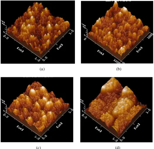
Figure 1 shows AFM images of the samples grown at different bias voltage. From these figures, it was ob-served that the grain size increases as a function of the bias voltage. Table 1 shows values of roughness, grain size and thickness for layers of TiAlN as a function of bias Vs. Although the sputtering techniques tend to produce denser coatings compared with other techniques used for surface treatments, the triode magnetron sputtering produces an increase in the ionization rate that combined with the high ionic energy and the refer-ence potential of the substrate generate a decrease in the substrate thickness caused by the energy saturation [18, 22]. The decrease of the thickness can be also attributed to the next factors: the first factor considered is the inverse pulverization process, which normally appears when the high ionic bombardment forces the ac-tive species (ionized atoms) to interact with other ions. If the energy level if these ions that bombard the sur-face is increased a desorption of the sursur-face atoms can be produced. This phenomenon can produce porous and surface defects [17]. The second factor is the increment of the collisions that, due to the ionization degree of the elements, the particles can become neutral and the magnetic field does not affect the movement; due to this effect, the particles do not possess the enough energy for arriving to the surface or for being adsorbed.
118
(a) (b)
(c) (d)
Figure 1: AFM images of TiAlN coatings for Vs (a) -40 V, (b) -70 V, (c) -100 V and (d) -150 V
Mechanical properties
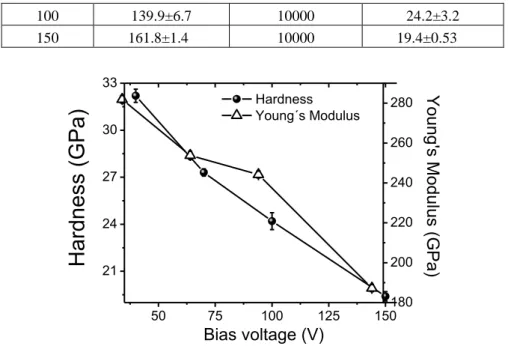
Fig. 2 shows the hardness and Young’s modulus of the TiAlN coatings as functions of the bias voltage. A decrease in the hardness was observed from 32 GPa to 19 GPa as is also shown in table 2. The Young’s modulus decreased from 282 GPa to 177 GPa when Vs was varied from -40 V to -150 V. These properties depend strongly on the percentage of Al that is present in the compound [23]. For values of Al close to 25%, the samples exhibited a higher hardness, which was caused by the deformation of the FCC structure, confirm-ing the results that were reported by ZHOU [24]. The decrease in hardness as a function of Vs can be attribut-ed to two phenomena: the first phenomenon is the increase in the grain size due to the higher mobility of the-atoms that arrives to the substrate surface, which can contribute to a reduction in hardness according to the relation described by Hall-Petch. This relation states that a decrease in the grain size increases the material toughness, as described by the LOPEZ [25]. The second phenomenon is the inclusion of Al atoms in the crys-tallographic lattice, which affects the elasticity modulus of the material when the inclusion is large enough because the stress in the crystalline structure will relax when the material is saturated, thus producing a de-crease in the mechanical properties [26].
Table 2: Penetration depth, average load and averad hardness for the samples grown at diferent VS.
SAMPLE PENETRATION DEPTH (nm)
AVERAGE LOAD (µN)
AVERAGE HARDNESS (Gpa)
40 125.9±3.069 10000 32.2±2.09
119
100 139.9±6.7 10000 24.2±3.2
150 161.8±1.4 10000 19.4±0.53
50 75 100 125 150
21 24 27 30 33
180 200 220 240 260 280
Bias voltage (V)
H
a
rd
n
e
ss
(G
Pa
)
Hardness Young´s ModulusYo
u
n
g
's
Mo
d
u
lu
s
(G
Pa
)
Figure 2: Hardness and Young’s modulus as functions of the bias voltage for the TiAlN coatings.
The ratio H3/E2 is an important parameter for studying the behavior of tribological properties; this re-lation is an indicator of the resistance of the layer to plastic deformation [27]. In Fig. 3, the dependence of H3/E2 (Fig. 3(a)) and the critical load (Fig. 3(b)) on the bias voltage can be seen. A decreasing tendency with Vs was observed, which corresponds to variations in the hardness and Young’s modulus. High values of H3/E2 can be beneficial for the wear resistance, as was stated by BEAKE, because this behavior provides a greater elastic deformation, thus enabling the coatings to remain in the elastic limit when overloads are ap-plied [28]. A decrease in the critical load from 52 N to 20 N was observed. This result is related to the varia-tions in the mechanical properties that were described before and to the adhesion between the coatings and the substrate.
Figure 3: H3/E2 relation and critical load as functions of the bias voltage for the TiAlN coatings.
Wea r and friction
The behavior of the coefficient of friction, COF, and the wear (volume of material per distance that was removed during the wear tests) in the case of TiAlN coatings that were grown with various bias voltages
40 60 80 100 120 140 160 0,20
0,25 0,30 0,35 0,40
H
3 /E
2
Bias Voltage (V)
(a)
40 80 120 160
20 30 40 50
C
ri
ti
ca
l
L
o
a
d
(N
)
Bias Voltage (V)
120 are shown in Figs. 4(a) and 4(b), respectively. The coating that was grown at Vs= -40 V exhibits the lowest COF value and the smallest wear. The coatings that were grown under these conditions also exhibit the high-est hardness and the lowhigh-est roughness. During the ball-on-disc thigh-est (BOD), in the first meters of the sliding distance, a polishing of the asperities occurs, which generates particles that are left in the edge of tracks. These particles are possibly produced because of the asperities of the coatings or the natural wear of the counter body. The particles that are on the track can produce greater wear, thus generating delamination and the removal of the protective layer. These particles might lead to a slightly larger volume loss [29].
Figure 4: (a) COF and (b) wear as functions of the bias voltage for the TiAlN coatings.
In Fig. 4, the COF dependence on the sliding distance (Fig. 5(a)), the wear track profile (Fig. 5(b)), the micrograph of the wear track at 25 m (Fig. 5(c)), the EDS spectrum of the track (Fig. 5(d)), the wear tracks at 50 m (Fig. 5(e)), 75 m (Fig. 5(f)) and 100 m (Fig. 5(g)) are shown for the samples that were grown at Vs=-40 V. A slight increase in the COF (Fig. 5(a)) during the polishing of the asperities can be observed because wear particles are produced. These particles belonged to the coating according to the EDS analysis (Fig. 5(d)). No abrupt transition is observed in the friction curves, i.e., these curves exhibit a steady state. These wear particles have a granular shape, thus causing a rolling effect and the stability of the curve (Fig. 5(a)). Accord-ing to the micrographs, as the slidAccord-ing distance is increased, wear particles are accumulated in the tracks, as observed for the sliding distances of 25 and 50 m (Figs. 5(c) and 5(e)). Two major frictional force sources of the sliding friction are the adhesion force that develops at the contact areas between the two surfaces and the deformation force that is required to plough the asperities of the harder surface through those of the softer surface [30]. At 75 and 100 m (Figs. 5(f) and 5(g)), a clean surface is observed. The behavior of the coatings over the total sliding distance showed that the coatings can endure the load conditions that were applied be-cause the volume of wear was not high enough to produce the total wear of the coating during the test accord-ing to the wear track profile (Fig. 5(b)).
0 20 40 60 80 100
0.0 0.3 0.6 0.9 1.2 1.5 C o e ff ici e n t o f F ri ct io n (µ )
Sliding Distance (m) (a)
0,0 0,1 0,2 0,3 0,4
-1500 -1000 -500 0 500 1000 1500 D e p th (n m)
Track Profile (µm) (b)
40 80 120 160
0,85 0,90 0,95 C o e ff ici e n t o f F ri ct io n (µ )
Bias Voltage (V) (a) 0 1 2 3 4 W e a r Vo lu me (mm 3 /N m)
121
(c) (d)
(e) (f) (g)
Figure 5: (a) Coefficient of friction (COF) curve for Vs= -40 V. (b) the wear track profile. (c) Micrograph of the wear track for the grown sample at 25 m; (d) EDS spectrum of the track. Micrographs of the wear tracks for the grown sample at (e) 50 m, (f) 75 m and (g) 100 m.
In Fig. 6, the COF dependence on the sliding distance (Fig. 6(a)), the wear track profile (Fig. 6(b)), the micrographs of the wear tracks at 25 m (Fig. 6(c)), 50 m (Fig. 6(d)), 75 m (Fig. 6(e)) and 100 m (Fig. 6(f)) are shown for the samples that were grown at Vs=-70 V. In Fig. 6(a), a zone in which the COF is constant (less than 50 m) is observed. In this region, the surface asperities of the coatings were plowed by the ball (Fig. 6(c)); afterwards, the surface was polished (Fig. 6(d)). The subsequent decrease in the COF could be caused by the low shear resistance of the highest regions of the surface, which would increase the contact area be-tween the tribological pair. At 70 m (Fig. 6(e)), an abrupt change in the curve, which is caused by the delam-ination of the coating, is observed. Stabilization is then observed in the system because the coating was al-most totally removed, as shown in Fig. 6(f).
0 20 40 60 80 100
0.0 0.3 0.6 0.9 1.2 1.5
C
o
e
ff
ici
e
n
t
o
f
F
ri
ct
io
n
(µ
)
Sliding Distance (m) (a)
0,0 0,1 0,2 0,3 0,4
-1500 -1000 -500 0 500 1000 1500
D
ep
th
(n
m)
Track Width (µm) (b)
100 m 75 m
50m
122 (c) (d)
\
(e) (f)
Figure 6: (a) Coefficient of friction (COF) curve for Vs= -70 V. (b) the wear track profile. Micrographs of the wear tracks for the grown sample at (c) 25 m, (d) 50 m, (e) 75 m and (f) 100 m.
In Fig. 7, the COF dependence on the sliding distance (Fig. 7(a)), the wear track profile (Fig. 7(b)) the micrographs of the wear tracks at 25 m (Fig. 7(c)), 50 m (Fig. 7(d)), 75 m (Fig. 7(e)) and 100 m (Fig. 7(f)) are shown for the samples that were grown at Vs=-100 V. Instability is observed in the COF at approximately 10 m, as shown in Fig. 7(a). This behavior occurs because the angular wear particles are trapped in the tribo-logical pair (Fig. 7(c)). The decrease in the COF is attributed to the removal of these particles and to the pres-ence of a smooth surface (Figs. 7(d) and 7(e)). The abrupt change in the curve after 80 m indicates the delam-ination of the layer, and the curve exhibits COF values for the substrate-ball contact. The rapid increase in the friction coefficient may be attributed to the initiation of a gross coating delamination event [30], as observed in the micrograph in Fig. 7(f), in which significant layer damage is shown. This damage is caused by the wear particles in the track, which increase the plowing by a third body [31]. According to observations by DMITRIEV [32], dry friction is largely determined not by the properties of the friction materials of the con-tacting pair but by the characteristics of the structure and composition of the third body or friction film. As long as third body films separate the first bodies (coating and disc), it is quite clear that the friction will be controlled by the sliding behavior of the films rather than by the properties of the first bodies [33]. This slid-ing behavior can increase the volume of the wear material, as observed in the wear track profile (Fig. 7(b)). In the current investigation, the friction coefficient was not constant during the test (Fig. 8(a)). The coeffi-cient of friction increased abruptly with compound layer delamination. The friction curve can be divided into two steps. Step 1 is related to the outmatching and smoothing of the sliding surfaces; hence, the friction coef-ficient decreased. After the removal of the compound layer, a breakthrough was observed in the friction curve. The breakthrough from step 1 to 2 normally indicated that the compound layer was completely worn out, so wear began first in the diffusion zone and then in the Ti–6Al–4V alloy, which produced an average friction coefficient of approximately 0.46 and noisier traces. These noisy traces are associated with the pres-ence of small grooves on the wear surface. RAUTRAY [34] observed 2 steps for the friction behavior of a nitrogen-implanted Ti–6Al–4V alloy. Conversely, MOLINARI [35] reported 3 or 4 steps for the friction be-havior of the same nitrided material.
100 m
50 m
123
0 20 40 60 80 100
0.4 0.5 0.6 0.7 0.8 0.9 1.0
C
o
e
ff
ici
e
n
t
o
f
F
ri
ct
io
n
(µ
)
Sliding Distance (m)
(a)
0,0 0,1 0,2 0,3 0,4
-1500 -1000 -500 0 500 1000 1500
D
e
p
th
(n
m)
Track Wide (µm) (b)
(c) (d)
(e) (f)
Figure 7: (a) Coefficient of friction (COF) curve for Vs= -100 V. (b) the wear track profile. Micrographs of the wear tracks for the grown sample at (c) 25 m, (d) 50 m, (e) 75 m and (f) 100 m.
124
0 20 40 60 80 100
0.0 0.2 0.4 0.6 0.8 1.0 1.2 1.4
C
o
e
ff
ici
e
n
t
o
f
F
ri
ct
io
n
(µ
)
Sliding Distance (m) (a)
0,0 0,1 0,2 0,3 0,4
-1500 -1000 -500 0 500 1000 1500
D
e
p
th
(n
m)
Track Wide (µm) (b)
(c) (d)
(e) (f)
Figure 8: (a) Coefficient of friction (COF) curve for Vs= -150 V. (b) the wear track profile. Micrographs of the wear tracks for the grown sample at (c) 25 m, (d) 50 m, (e) 75 m and (f) 100 m.
In summary, except for the case of the films that were grown at Vs=-100 V, the COF remains stable depending on the sliding distance, the presence of third bodies and film delamination. The films that were grown at Vs=-40 V exhibited the lowest COF and wear volume. The coatings that were grown under these conditions also exhibited the highest hardness and the lowest roughness. This behavior can be attributed to the lower energy of the particles that impacted the substrate and films, thus producing less damage, and to the stress relaxation that was caused by the inclusion of smaller atoms (Al) in the lattice, according to the results presented in [17].
4. CONCLUSIONS
TiAlN coatings were produced using the triode magnetron sputtering technique to investigate the effect of the bias voltage on the mechanical and tribological properties of the coatings. It was observed that the hardness and Young´s modulus of the coatings decreases as a function of the grain size, following the Hall-Petch rela-tion. An increase in the Al concentration led to reductions in the hardness and Young´s modulus; this behav-ior was associated with the saturation of the crystalline structure. The coefficient of friction (COF) values oscillated between 0.7 and 0.9; these values are in agreement with the results that were previously reported in the literature for this material. The most dominant wear mechanism was the abrasion that was associated with the wear particles, which act as a third body. This analysis enables the conclusion that the film that was grown at Vs=-40 V exhibited the best mechanical and tribological behavior.
100 m 75 m
125 5. ACKNOWLEDGMENTS
The authors gratefully acknowledge the financial support of the División para la Investigación de la
Univer-sidad Nacional de Colombia Sede Manizales (DIMA) under the project “Producción y caracterización de recubrimientos con aplicaciones industriales y biocompatibles.”
6. BIBLIOGRAPHY
[1] KIM, D., CAO, D., BRYANT, M.D., et al., “Tribological study of microbearing for MEMS applications”, Journal of Tribology, v. 127, n.3, pp. 537-547, Jan. 2005.
[2] MYSHKIN, N.K., “Devices for Tribotests at Micro/Nano Scale”, Tribology Industry, v. 26, n. 2, pp. 15-20. 2004.
[3] LEYENDECKER, T., LEMMER, O., ESSER, S., et al., “The development of the PVD coating TiAlN as
a commercial coating for cutting tools”, Surface and Coatings Technology, v. 48, n.1, pp. 175-178, Nov. 1991.
[4] UPADHYAY, R. K., KUMARASWAMIDHAS, L.A., “Friction behaviour of TiN, CrN coating on AISI
4320 steel substrate”, International Journal Mechanical Engineering and Robotics Research, v. 2, n. 1, pp. 107-109, Jan. 2013.
[5] RECCO, A.A.C., TSCHIPTSCHIN, A.P., “Structural and Mechanical Characterization of Duplex Multi-layer Coatings Deposited onto H13 Tool Steel”, Journal of Materials Research and Technology, v. 1, pp. 182-188, Oct. 2012.
[6] SVEEN, S., ANDERSSON, J.M., M’SAOUBI, R., OLSSON M., “Scratch adhesion characteristics of
PVD TiAlN deposited on high speed steel, cemented carbide and PCBN substrates”, Wear, v.308, pp. 133-141, Sep. 2013.
[7] RAMADOSS, R., KUMAR, N., PANDIAN, R., et al., “Tribological properties and deformation mech
a-nism of TiAlN coating sliding with various counterbodies”, Tribology International, v. 6, pp. 143-149, May 2013.
[8] JEONA, S., VAN TYNE, C.J., LEE, H., “Degradation of TiAlN coatings by the accelerated life test using
pulsed laser ablation”, Ceramics International, v. 40, pp. 8677-8685, Jan. 2014.
[9] TILLMANN, W., SPRUTE, T., HOFFMANN, F., CHANG, Y., et el., “Influence of bias voltage on residual stresses and tribological properties of TiAlVN-coatings at elevated temperatures”, Surface and Coa t-ings Technology, v. 231, pp. 122-125, March 2013.
[10] YUAN, L., GAO, Y., ZHANG, W., et al., “Effect of Negative Bias Voltage on Corrosion Resistance of
TiN Coating Deposited by MAIP”, Advanced Materials Research, v. 399-401, pp. 1898-1902, Nov. 2011.
[11] DETOR, A.J., HODGE A.M., CHASON E., et al., “Stress and microstructure evolution in thick spu
t-tered films”, Acta Materialia, v. 57, pp. 2055–2065, Journal of Vacuum Science & Technology A, v. 21, pp. 117-128, Feb. 2009.
[12] LJUNGCRANTZ, H., HULTMAN L., et al., “Ion induced stress generation in arc-evaporated TiN
films”, Journal of Applied Physics, v. 78, n.2, pp. 832-837, July 1995.
[13] DETOR, A.J., HODGE, A.M., CHASON, E., et al., “Stress and microstructure of thick sputtered films”. Acta Materialia, v. 57, n. 7, pp. 2055-2065, April 2009.
[14] ZHAO H., WANG, X., LIU Q., et al, “Structure and wear resistance of TiN and TiAlN coatings on
AZ91 alloy deposited by multi-arc ion plating”, Transactions of Nonferrous Metals Society of China, v. 20, pp. 679-682, Jan. 2010
[15] ALIAJ, F., SYLA, N., “Influence of Al content and bias voltage on the microstructure of Ti1-xAlxN
hard coatings”, Journal of Engineering and Applied Sciences, v. 5, pp. 394-402, 2010.
[16] KONG, Q., JI, L., LI, H., et al., “Influence of substrate bias voltage on the microstructure and residual stress of CrN films deposited by medium frequency magnetron sputtering”, Materials Science and Engineer-ing: B, v. 176, n. 11, pp. 850-854, June 2011.
[17] DEVIA, D.M., RESTREPO-PARRA, E., ARANGO, P.J., et al., “TiAlN coatings deposited by triode
magnetron sputtering varying the bias voltage”, Applied Surface Science, v. 257, n. 14, pp. 6181-6185, May 2011.
[18] RECCO, A.C.C., OLIVEIRA, I.C., MASSI, M., et al., “Adhesion of reactive magnetron sputtered TINx
126 Dec. 2007.
[19] Devia, D.M., Restrepo-Parra, E., Velez-Restrepo, J.M., “Structural and Morphological Properties of
Titanium Aluminum Nitride Coatings Produced by Triode Magnetron Sputtering”, Ingeniería y Ciencia, v. 10, n. 20, pp. 51-64, July 2014.
[20] HUTAŘ, P., NÁHLÍK, L., ŠESTÁKOVÁ, L., et al., “A fracture mechanics assessment of surface cracks existing in protective layers of multi-layer composite pipes”, Composite Structures, v. 92, n. 5, pp. 1120-1125, April 2010.
[21] PALDEY, S., DEEVI, S.C., “Single layer and multilayer wear resistant coatings of (Ti,Al)N: a review”,
Materials Science and Engineering: A, v. 342, n. 1, pp. 58-79, Feb. 2003.
[22] CAICEDO, J.C., AMAYA, C., GÓMEZ, M.E., et al., “Dependencia de las propiedades mecánicas de
TiC1-xNx con el voltaje Bias”, Revista Latinoamericana de Meta lurgia y Materiales, v. 4, pp. 1487-1492, July 2009.
[23] YOON, J.S., LEE, H.Y., HAN, J.G., et al., “The effect of Al composition on the microstructure and m e-chanical properties of WC–TiAlN superhard composite coating”, Surface and Coatings Technology, v.142-144, pp. 596-602, July 2001.
[24] ZHOU, M., MAKINO, Y., NOSE, M., et al., “Phase transition and properties of Ti–Al–N thin films prepared by r.f.-plasma assisted magnetron sputtering”, Thin solid Films, v. 339, n. 1, pp. 203–208, Feb. 1999.
[25] LÓPEZ, J.M., GORDILLO-VÁZQUEZ, F.J., BÖHME, O., et al., “Low grain size TiN thin films o
b-tained by low energy ion beam assisted deposition”, Applied Surface Science, v. 173, n. 3, pp.290-295, March 2001.
[26] EBERHARDT, A.W., PANDEY, R., WILLIAMS, J.M., et al., “The roles of residual stress and surface
topography on hardness of Ti implanted Ti6Al4V”, Materials Science and Engineering: A, v. 229, n. 1, pp. 147-155, June 1997.
[27] BEAKE, B.D., VISHNYAKOV, V.M., HARRIS, A.J., “Relationship between mechanical properties of
thin nitride-based films and their behaviour in nano-scratch tests”, Tribology International, v. 44, n. 4, pp. 468–475, April 2011.
[28] BEAKE, B.D., RANGANATHAN, N., “An investigation of the nanoindentation and nano/micro
-tribological behaviour of monolayer, bilayer and trilayer coatings on cemented carbide”, Materials Science and Engineering: A, v. 423, n. 1, May 2006.
[29] BAKSHI, S.R., WANG, D., PRICE, T., et al., “Microstructure and wear properties of alum i-num/aluminum–silicon composite coatings prepared by cold spraying”, Surface and Coatings Technology, v. 204, n. 4, pp. 503–510, Nov. 2004.
[30] FUJISAWA, N., SWAIN, M.V., JAMES, N.L., et al., “Carbon coating of Ti-6Al-4V for reduced wear in
combined impact and sliding applications”, Tribology International, v. 36, n. 12, pp. 873–882, Dec. 2003.
[31] FU, Y., WEI, J., BATCHELOR, A.W., “Some considerations on the mitigation of fretting damage by
the application of surface-modification technologies”, Journal of Materials Processing Technology, v. 99, n. 1, pp. 231-245, March 2000.
[32] DMITRIEV, A.I., ÖSTERLE, W., KLOß, H., ORTS-GIL, G., “A study of third body behaviour under dry sliding conditions comparison of nanoscale modelling with experiment”, Estonian Journal of Engineer-ing, v. 18, pp. 270–278, July 2012.
[33] HINRICHS, R., SOARES MARCIO, R.F., LAMB, R.G., VASCONCELLOS, M.A.Z., “Phase chara c-terization of debris generated in brake pad coefficient of friction tests”, Wear, v. 270, pp. 515-519, March 2011.
[34] RAUTRAY, T. R., NARAYANAN, R., KIM, K. H., “Ion implantation of titanium based biomaterials”,
Progress in Materials Science, v. 56, pp. 1137–1177, March 2011.
[35] MOLINARI, A., STRAFFELINI, G., TESI, B., et al., “Effects of load and sliding speed on the tribolo