Universidade do Minho
Escola de Ciências
Paulo Miguel Babo Cunha Salvador
Deposition and characterization of CdS and
ZnO:Al thin films for Cu(In,Ga)Se solar cells
2Paulo Miguel Babo Cunha Salvador
Deposition and characterization of CdS and ZnO:Al t
hin films for Cu(In,Ga)Se
Universidade do Minho
Escola de Ciências
Paulo Miguel Babo Cunha Salvador
outubro de 2016
Deposition and characterization of CdS and
ZnO:Al thin films for Cu(In,Ga)Se solar cells
2Trabalho realizado sob orientação do
Professor Dr. João Pedro Santos Hall Agorreta Alpuim
e do
Dr. Sascha Sadewasser
Dissertação de Mestrado,
Mestrado em Física Aplicada
A
CKNOWLEDGMENTS
Firstly, I want to express my sincere thanks to my practical tutor Dr. Pedro Salomé, whose support was indeed exceptional, for his constant patience and guidance throughout the entire work, and for his profound knowledge on each small step of this thesis. Also, my sincere appreciations to my INL tutor Dr. Sascha Sadewasser, head of the LaNaSC (laboratory for nanostructured solar cells) group at INL, whose council, support and funding were fundamental to the fulfilment of this work. I would like to thank Professor Pedro Alpuim, who accepted to be my Universidade do Minho Supervisor and whose trust and confidence certainly assured possible the development of this project.
I also want to thank Dr. Nicoleta Nicoara, also member of the LaNaSC group, for the provided help in obtaining AFM imaging and in the CdS holder’s design; Dr. Miriam Debs for the training and assistance provided during the XRD measurements, and Engineering Physics student Miriam Ahlberg for the aid on electrical and quantum efficiency measurements performed on the CIGS solar cells.
I am also truly appreciated for the warm environment created by all the remaining LaNaSC members, Dr. Kamal Abderrafi, Dr. Vanessa Iglesias and Dr. Rodrigo Andrade, and by all the remaining INL members.
Finally, the acknowledgment of my gratitude to my parents and brother, who always strongly supported me and encouraged me to keep on working forward throughout my academic path.
A
BSTRACT
The purpose of this thesis is to establish a baseline methodology for the optimized deposition of CdS thin films by chemical bath deposition (CBD) and ZnO:Al thin films by atomic layer deposition (ALD), for the development of Cu(In,Ga)Se2 (CIGS) solar cells at INL facilities. A background research on
several optimized parameters is presented and taken in consideration for both layers’ growth methodologies.
A detailed study on how the chemical bath deposition parameters affect the properties of the resulting CdS thin film is made. The reproducibility of CdS layers with thickness 50-70 nm is successfully shown. The studied parameters that were found to heavily affect the deposition were: i) the bath temperature; ii) the pH (indirectly, through the amount of ammonia); iii) the deposition time. A colour-thickness pattern established a naked-eye projection of the grown sample’s thickness, which allows for a quick and quantitative evaluation of the deposited films. Further XRD measurements are presented, as well as a statistical particle analysis with the software ImageJ applied to optical microscopy images of the samples. Based on these analysis, a modelling for the transition between ion-by-ion deposition and cluster-by-cluster deposition was presented. Further works compass the development of a working sample holder and the production of a detailed experimental protocol.
Concerning the ZnO:Al depositions, ALD, which is a potential industrial friendly technique, was used. The study focused on evaluating the growth rates of the system and on understanding the thickness effects on the transmittance and resistance of the resultant films. Two aluminium doping quantities were also studied and an increase of the bandgap energy is confirmed with increasing aluminium doping. The sample with the lowest sheet resistance of 80 Ω.□-1 of this work had a thickness of 735 nm, while
presenting transmittance values averaging above 90 % for wavelengths values between 400-1200 nm. As part of understanding the thickness effects, scanning electron microscopy, atomic force microscopy and X-ray diffraction analysis were performed, revealing a correlation between the (110) planar orientation and the resistivity values.
Both CdS and ZnO:Al layers are then individually incorporated in (externally manufactured) CIGS solar cells and are characterized. The solar cell results showed that the CIGS layer does not survive the harsh growth conditions of the ALD processing, which demonstrates that more improvements in this technique are needed. Two solar cell devices with 60 nm and a 210 nm CdS layers present fill factors of 0.60 and 0.50 respectively, and efficiency values of 11.6 % and 9.8 %. These results demonstrate better electrical performances for the solar cell with the optimized 60 nm CdS layer, presenting an increase of 1.8 % efficiency with a 150 nm decrease in thickness, highlighting the importance of controlling the CdS deposition procedure.
R
ESUMO
Esta tese tem como objetivo estabelecer uma metodologia de base para o crescimento otimizado de filmes finos de CdS por deposição em banho químico (CBD) e de ZnO:Al por atomic layer deposition (ALD), com o intuito de otimizar células solares de Cu(In,Ga)Se2 (CIGS) nas infraestruturas do INL.
Uma pesquisa base na otimização de vários parâmetros base é apresentada, considerando os respetivos métodos de deposição e materiais.
É efetuado um estudo detalhado na influência dos parâmetros de deposição do banho químico nas propriedades dos filmes de CdS resultantes. A reprodutibilidade da deposição de uma camada de 50-70 nm de espessura é assegurada. Os parâmetros estudados que mais afetam a deposição são: i) a temperatura; ii) o pH (indiretamente, a partir da quantidade de amónia); iii) o tempo da deposição. É estabelecido um padrão entre a cor do filme e um alcance de espessuras, para permitir uma aproximação rápida e quantitativa da espessura da amostra a olho nu. São apresentadas medidas de difração de raios-X, juntamente com uma análise estatística de partículas através do software ImageJ a imagens das amostras, recolhidas por microscopia ótica. Também foram desenvolvidos um suporte de substratos para a deposição e um protocolo experimental detalhado para o processo de CBD.
Para os filmes de ZnO:Al foi utilizada a técnica de ALD, que é uma técnica potencialmente amiga da indústria. Este estudo foca-se em avaliar os rácios de crescimento do sistema e em compreender os efeitos da espessura na transparência e na resistência dos filmes resultantes. Foram utilizadas duas diferentes quantidades de dopagem com alumínio, e foi confirmado um aumento na energia de hiato com o aumento de percentagem de alumínio nos filmes. A amostra com resistividade de folha inferior deste trabalho, com 80 Ω.□-1, possuía 735 nm de espessura e apresentava uma média de valores de
transmitância acima de 90 %, para comprimentos de onda compreendidos entre 400-1200 nm. Para compreender os efeitos da espessura nos filmes, utilizou-se microscopia eletrónica de varrimento, microscopia de força atómica e difração de raios-X, que revelaram uma correlação entre a orientação planar (110) e os valores de resistividade obtidos para cada amostra.
Ambos os filmes de CdS e de ZnO:Al são incorporados individualmente em células solares CIGS, externamente produzidas, e são caracterizadas. Os resultados das células solares demonstraram que a camada CIGS não sobrevive às condições severas do processo de ALD, o que revela que são necessários mais desenvolvimentos para esta técnica de deposição. Duas células solares com incorporação de CdS com espessuras de 60 nm e 210 nm apresentam valores de fill factor de 0.60 e 0.50, respetivamente, e eficiências de 11.6 % e 9.8 %. Estes resultados demonstram uma performance elétrica melhorada para a camada otimizada de CdS com 60 nm, apresentando um aumento de 1.8 % de eficiência com a redução de 150 nm de espessura, evidenciando a importância do controlo do processo de deposição de CdS. Palavras-chave: Semicondutores, Células solares de filmes finos, CdS buffer, ZnO:Al óxido condutor e
I
NDEXAcknowledgments ... iii
Abstract ... v
Resumo ... vii
List of figures ... xiii
List of tables ... xvii
List of abbreviations, initials and acronyms ... xix
Introduction ... 1
1. Motivation and objectives ... 1
2. Solar cell device topics ... 1
2.1 Band structure background ... 1
2.2 Electron-hole pairs generation and recombination processes ... 3
2.3 Doping semiconductors and the p-n junction ... 4
2.4 Current extraction mechanism ... 6
2.5 Ideal diode and the solar cell characterization ... 6
3. Cu(In,Ga)Se2 solar cell ... 11
3.1 Substrate and back contact ... 12
3.2 CIGS absorber layer ... 13
3.3 Buffer layer ... 13
3.4 Shunt preventing layer ... 14
3.5 Transparent conductive oxide ... 14
3.6 Grid ... 15
4. Background ZnO:Al TCO and CdS buffer layer considerations ... 17
4.1 CdS buffer layer... 17
4.2 ZnO:Al TCO ... 19
5. Experimental techniques ... 23
5.1 Chemical bath deposition ... 23
5.1.1 CdS growth by chemical bath deposition ... 25
5.2 Atomic layer deposition... 26
5.2.1 ZnO:Al growth by atomic layer deposition ... 30
x 5.5 X-ray diffraction ... 35 5.6 Optical spectroscopy ... 37 5.6.1 Transmittance measurements ... 37 5.6.2 Swanepoel method ... 39 5.7 Contact profilometry... 40 5.8 Four-point probe ... 41 5.8.1 Methodology ... 42
Results and Discussion ... 45
6. CdS results ... 45
6.1 Evolution of the bath temperature experiment ... 46
6.2 Calibration experiments ... 47
6.2.1 Series 1 – Reproducibility test ... 49
6.2.2 Series 2 – Time variation series ... 50
6.2.3 Series 3 – Outer bath temperature series ... 52
6.2.4 Series 4 – Ammonia series ... 54
6.2.5 Series 5 – Deposition bath water volume series ... 56
6.2.6 Series 6 – Cadmium acetate series ... 58
6.2.7 Series 7 – Two parameters’ small variation ... 60
6.3 Colour-thickness relation ... 61
6.4 Grazing incidence XRD ... 62
6.5 Statistical particle analysis... 65
7. ZnO:Al results ... 69 7.1 Optical spectroscopy ... 69 7.1.1 Bandgap calculation ... 71 7.1.2 Thickness assessments ... 72 7.1.3 Deposition rate ... 74 7.2 Resistivity ... 75
7.3 SEM and AFM... 76
7.4 XRD ... 80
7.4.1 Bragg’s law ... 83
7.4.2 Hexagonal structure equation ... 84
7.4.3 Sherrer equation ... 86
8.1 J-V curves ... 88
8.1.1 ZnO:Al – solar cell A ... 88
8.1.2 CdS – Solar cells B and D ... 90
8.2 External quantum efficiency ... 91
9. Conclusions ... 93
10. Future work ... 95
References ... 97
Annex I – CdS substrate holder design ... 105
L
IST OF FIGURES
Figure 1 – Energy splitting electrical configuration schematization of an n-atom system [7]. . 2
Figure 2 – Recombination processes illustrated [10]. ... 4
Figure 3 – P-n junction illustrated [12]. ... 5
Figure 4 – P-n homojunction band structure schematically represented. CBM, EF and VBM correspond to the conduction band minimum, the Fermi energy and the valence band maximum, respectively [13]. ... 6
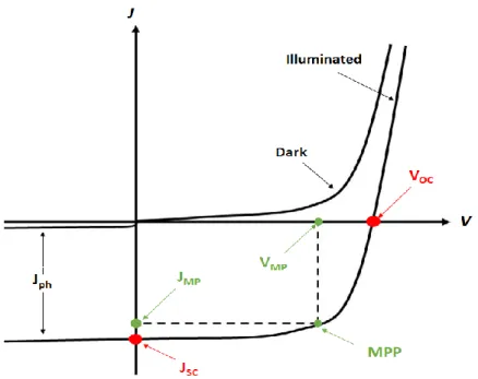
Figure 5 – Typical solar cell J-V plot, under illumination and in the dark. Main features highlighted: Voc (open-circuit voltage), Jsc (short-circuit current density), Vmp (maximum power voltage), Jmp (maximum power current density) and MPP (maximum power point) [16]. ... 8
Figure 6 – Typical CIGS stack structure, not to scale. ... 11
Figure 7 – CIGS heterojunction band diagram as discussed by the research group EMPA, not to scale [19]. ... 12
Figure 8 – Schematic representation of the processes which could lead to the deposition of a thin film. [71]. ... 24
Figure 9 – Equipment used for CBD depositions. ... 26
Figure 10 – One ALD cycle process, description below [77]. ... 28
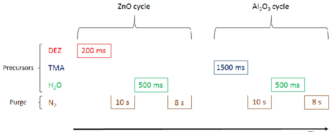
Figure 11 – Precursors’ and purging gases’ timeline for the ALD process. ... 30
Figure 12 – Beneq TFS 200 ALD equipment [87]. ... 31
Figure 13 – Schematized AFM apparatus [89]. ... 32
Figure 14 – AFM equipment, Bruker-Dimension Icon. ... 33
Figure 15 – Main SEM system schematization [90]. ... 33
Figure 16 – Shape of electron interaction volume and signals generated within a sample [93]. ... 34
Figure 17 – SEM equipment Quanta FEG 650. ... 35
Figure 18 – X’Pert PRO PANalytical XRD equipment. ... 36
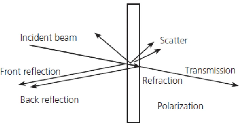
Figure 19 – Light-solid interaction phenomena [95]. ... 37
Figure 20 – Schematic illustration of the optical path inside the spectrometer. ... 38
Figure 21 – PerkinElmer UV/VIS/NIR Spectrometer Lambra 950. ... 38
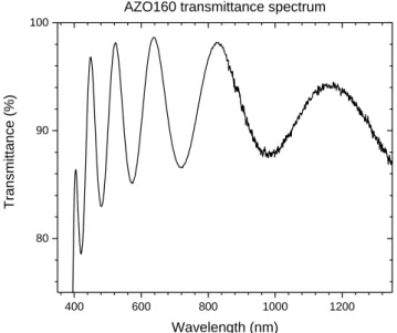
Figure 22 – Transmittance spectrum, TR(λ), of the sample AZO160. ... 39
xiv
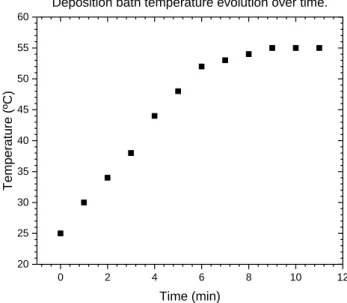
Figure 25 – Four-point probe equipment. ... 42 Figure 26 – Deposition bath temperature evolution overtime. ... 46 Figure 27 – Deposition bath colour evolution with time. Outer bath colour change due to camera contrast. ... 47 Figure 28 – S1 series grown. Middle marks correspond to the taped areas for thickness measurements. ... 49 Figure 29 – S1 and S2 graphical representation. Error bar for roughness. Red marked samples’ thickness deviate from expected margin of error. ... 51 Figure 30 – S2 samples grown. Middle/corner marks correspond to the taped areas for thickness measurements. ... 52 Figure 31 – S3 graphical representation. Error bar for roughness. ... 53 Figure 32 – S3 series grown. Middle/corner marks correspond to the taped areas for thickness measurements. ... 54 Figure 33 – S4 graphical representation. Error bar for roughness. ... 55 Figure 34 – S4 series grown. Middle/corner marks correspond to the taped areas for thickness measurements. ... 56 Figure 35 – S5 graphical representation. Error bar for roughness. ... 57 Figure 36 – S5 series grown. Middle marks correspond to the taped areas for thickness measurements. ... 58 Figure 37 – S6 graphical representation. Error bar for roughness. ... 59 Figure 38 – S6 series grown. Middle/corner marks correspond to the taped areas for thickness measurements. ... 59 Figure 39 – S7 series grown. Middle marks correspond to the taped areas for thickness measurements. ... 61 Figure 40 – Grown samples from each series. ... 61 Figure 41 – 11 minutes sample’s GIXRD data. 10 count offset for each 0.05º incident angle increment. ... 62 Figure 42 – 11 minute sample’s GIXRD data, incident angle w of 0.30º. Blue lines correspond to CdS matching peaks retrieved from the software. ... 63 Figure 43 – 11 minute sample’s GIXRD data, incident angle w of 0.45º. Blue and green lines correspond to CdS and Mo matching peaks retrieved from the software, respectively. ... 63 Figure 44 - 11 minute sample’s GIXRD data, incident angle w of 0.60º. Blue and green lines correspond to CdS and Mo matching peaks retrieved from the software, respectively. ... 64 Figure 45 – Optical microscopy imaging of the S2 series samples, 100x magnification. ... 65
Figure 46 – ImageJ analysis windows of the default sample. Background (brown) image is the original optical microscopy image. Bottom left area (red outline) is the chosen section of the image Top left (grey) area is the chosen area in 8-bit format. Bottom right window for the grain
threshold quantities to analyse. ... 66
Figure 47 – S2 particle average size relation with deposition time. ... 67
Figure 48 – S2 particle area percent relation with deposition time. ... 67
Figure 49 – Glass substrate transmittance spectrum. ... 70
Figure 50 – Transmittance spectra of ZnO:Al samples and Uppsala’s reference sample. Average transmittance (a.t.) (450-1200 nm wavelength range) in caption. ... 70
Figure 51 – ZnO:AL samples’ α2 vs hv curves. ... 71
Figure 52 – ZnO:Al samples’ thickness-ZnO cycle relation. ... 73
Figure 53 – ZnO:Al samples’ SEM imaging, 82 880x magnification. ... 77
Figure 54 – ZnO:Al samples’ SEM imaging, 414 400x magnification. ... 77
Figure 55 – ZnO:Al samples’ AFM imaging, 3x3 µm image size. ... 78
Figure 56 – ZnO:Al samples’ AFM imaging, 1x1 µm image size. ... 79
Figure 57 – AZO40 (240 nm) XRD data. Vertical blue lines correspond to the matching peaks found by software Highscore, corresponding to Zincite compound. ... 80
Figure 58 – AZO80 (400 nm) XRD data. Vertical blue lines correspond to the matching peaks found by software Highscore, corresponding to Zincite compound. ... 81
Figure 59 – AZO105 (410 nm) XRD data. Vertical blue lines correspond to the matching peaks found by software Highscore, corresponding to Zincite compound. ... 81
Figure 60 – AZO160 (735 nm) XRD data. Vertical blue lines correspond to the matching peaks found by software Highscore, corresponding to Zincite compound. ... 82
Figure 61 – CdS layers grown in Mo, during the CdS deposition of solar cells B and D. Middle marks correspond to the taped areas for thickness measurements. ... 88
Figure 62 – J-V curves (illuminated and dark) of two cells within sample A, A1 and A2. ... 89
Figure 63 – J-V curves (illuminated and dark) of two cells within sample B, B2 and B4. ... 90
Figure 64 – J-V curves (illuminated and dark) of two cells within sample D, D3 and D5. ... 90
Figure 65 – External quantum efficiency spectra of samples B and D. ... 91
Figure 66 – First sketch of the sample holder’s design. Highlight on the middle column passing through the top piece. Contrast applied. Not to scale. ... 105 Figure 67 – Autocad imaging of the developed sample holder design. Rear-side design of the top and bottom parts of the sample holder (top). Base-side design of the top part of the holder
xvi
Figure 68 – Powder measurement (left). Mixing the powder with deionized water (middle). Thiourea in the ultra-sound (right). ... 109 Figure 69 – Sample holder with two samples facing each other ... 109 Figure 70 – Measuring the ammonia (left). Ammonia, cadmium acetate, thiourea, from the right (right). ... 110 Figure 71 - Deposition beaker in the middle of the Outer Bath, stirring occurring. ... 110 Figure 72 – Deposited samples dipping in deionized water, front and lateral views (left). Drying the deposited sample with pumping nitrogen. ... 111
L
IST OF TABLES
Table 1 – Temperature evolution of the deposition bath overtime. Colour pattern for timeline assessment easiness. ... 46 Table 2 – Grown CdS series and the respective objectives. ... 48 Table 3 – Default parameters’ values. ... 48 Table 4 – Thickness and roughness measurements of series 1 samples. Values rounded to integer units. ... 49 Table 5 – Thickness and roughness measurement values of series 2 samples. Values rounded to integer units. Asterisk sample for comparison purposes. ... 50 Table 6 – Thickness and roughness measurement values of series 3 samples. Values rounded to integer units. Asterisk sample for comparison purposes. ... 53 Table 7 – Thickness and roughness measurement values of series 4 samples. Values rounded to integer units. Asterisk sample for comparison purposes. ... 55 Table 8 – Thickness and roughness measurement values of series 5 samples. Values rounded to integer units. ... 56 Table 9 – Thickness and roughness measurement values of series S6 samples. Values rounded to integer units. Asterisk sample for comparison purposes. ... 58 Table 10 – Thickness and roughness measurement values of series 3 samples. Values rounded to integer units. ... 60 Table 11 – CdS thickness-colour framework. Colour pattern for comparison purposes. ... 62 Table 12 – Highscore data analysis of S2 series 11 minute sample’s GIXRD measurements. Colour pattern for graphic assessment easiness. ... 64 Table 13 – Swanepoel parameters for each ZnO:Al sample. λ1 and n1 for the wavelength and
refractive index of the first peak chosen, λ2 and n2 for the respectives of the second peak chosen,
d for the thickness calculated. ... 72 Table 14 – Averaged optical and profilometry thickness of ZnO:Al samples. ... 74 Table 15 – Deposition rates calculated for ZnO:Al samples, considering optical thickness values and ZnO deposition cycles. ... 75 Table 16 – Sheet resistivity values obtained and calculated resistivity of ZnO:Al samples. ... 76 Table 17 – Average roughness of AFM images taken to the ZnO:Al samples. Colour pattern for comparison purposes. ... 79
xviii
Table 18 – Highscore data analysis of AZO40 sample’s XRD measurements. Colour pattern for comparison purposes. ... 80 Table 19 – Highscore data analysis of AZO80 sample’s XRD measurements. Colour pattern for comparison purposes. ... 81 Table 20 – Highscore data analysis of AZO80 sample’s XRD measurements. Colour pattern for comparison purposes. ... 81 Table 21 – Highscore data analysis of AZO80 sample’s XRD measurements. Colour pattern for comparison purposes. ... 82 Table 22 – Main peaks common to all ZnO:Al XRD’s measurements. ... 83 Table 23 – Interplanar distances, d, calculated from Bragg’s law for each main peak of every sample. Comparison with Highscore data. Colour pattern for comparison purposes. ... 84 Table 24 – Calculated hexagonal structure parameters for each peak of every sample. Highscore hexagonal structure parameters in the left, along with the respective sample. Colour pattern for comparison purposes. ... 85 Table 25 – Calculated mean size of the crystallites for 2θ peak of 31.8º for the AZO samples and the respective sample’s resistivity. ... 86 Table 26 – Solar cell samples’ developed layer, with respective deposition technique, deposition parameters and thickness measured in the duplicated sample. ... 87 Table 27 – Solar cell parameters of samples B and D. Averaged cell values for each solar cell sample: 5 inner cells for sample B, 2 inner cells for sample D. ... 91
L
IST OF ABBREVIATIONS
,
INITIALS AND ACRONYMS
AFM ALD CB CBD CBM CIGS CVD d DC DEZ e EF Eg EQE FF FWHM GIXRD GS h I IQE J Jph JSC k kB MPP n NA ND ne nf ơ pn PV PVDAtomic force microscopy Atomic layer deposition Conduction band Chemical bath deposition Conduction band minimum Cu(In,Ga)Se2
Chemical vapour deposition Interplanar distance Direct current Diethyl zinc Electron charge Fermi Energy Bandgap energy
External quantum efficiency Fill factor
Full width at half maximum Grazing incident X-ray diffraction Grain size
Planck’s constant Intensity
Internal quantum efficiency Current density
Photovoltaic current density Short-circuit current density Shape factor
Boltzmann constant Maximum power point Refractive index
Concentration of acceptors Concentration of donors Concentration of electrons
Concentration of free charge carriers Conductivity
Concentration of holes Photovoltaic
Physical vapour deposition
QE RF ri RS s SEM SLG SRH T t TCO TMA TR V VB VBI VBM VOC w XRD α β η λ μ ρ τ υ φ χ Quantum efficiency Radio-frequency Distance/radius Sheet resistivity
Substrate refractive index Scanning electron microscopy Sola-lime-glass
Shockley-Read-Hall Temperature Thickness
Transparent conducting oxide Trimethyl aluminium
Transmittance Voltage Valence band Built-in voltage
Valence band maximum Open-circuit voltage Depletion width X-ray diffraction Absorption coefficient Non-ideal factor Efficiency Wavelength Mobility Resistivity Crystallite size Frequency Potencial Absorbance
I
NTRODUCTION
1. M
OTIVATION AND OBJECTIVES
Nowadays, the need for clean renewable energies is no longer a novelty. The tradition fossil fuel sources play many negative roles on our society. Reports on global warming are increasing, due to the emission of green-house gases, and fossils’ supply and usage are not sustainable from economic and social perspectives. The answer for a better tomorrow dwell on the development of new and better clean energies to replace the “dirty” ones.
Photovoltaic cells, PV, commonly known as solar cells, are devices that directly transform solar light into direct current electricity, or DC. Among various kinds of renewable energy solutions, PV has attracted many attentions, due to its promising alternative advantages to other energy sources. Firstly, the sun is a reliable abundant energy source that constantly radiates an enormous amount of energy into Earth. Secondly, PV’s operation does not require any direct green-house emission, noise or any kind of pollution. Lastly, it is a very reliable energy conversion technique. With low maintenance costs and no moving parts, the main challenge is to develop solar cells with increasing efficiency and reduced industrial production costs. Thin film solar cells possess the advantage of requiring small amounts of materials, as the active photovoltaic layer of such cells has but a few micrometres of thickness. From within the broad range of thin film solar cell configurations and materials, Cu(In,Ga)Se2 solar cells, or CIGS for
short, present one of the most promising candidates.
CIGS is the material used as the absorber layer, i.e. the main layer that transforms the absorbed solar radiation into electricity, and is usually followed by a CdS buffer layer and an aluminium doped ZnO transparent conducting oxide (TCO) layer. These three layers are a common popular configuration, due to their excellent optical and electrical properties. Together, along with several other layer upgrades, this configuration has recently achieved a record certified performance of 22.6 % efficiency in ZSW, Zentrum für Sonnenenergie- und Wasserstoff-Forschung Baden- Württemberg, Germany [1].
The International Iberian Nanotechnology Laboratory, INL, has recently invested to help the scientific community to further develop the CIGS solar cells. The main objective of this thesis is to develop and understand a baseline growth procedures for the CdS buffer layer, aiming for thicknesses between 50-70 nm, and to evaluate the use of atomic layer deposition of the ZnO:Al
2
transparencies, while verifying if the deposition process does not harm the CIGS layer. The CdS baseline growth is performed with well-known chemical bath deposition, CBD, which stands the most promising deposition method for the buffer layer due to (still not completely understandable) better electrical performances over the CIGS stack solar cells. The ZnO:Al growth is performed with atomic layer deposition, ALD, as it is a most promising vacuum easy-to-scale deposition technique that produces thin films with great conformity. After optimization of these layers, they are introduced into CIGS solar cells, fabricated at Uppsala University, following the Ångström Solar Center baseline CIGS solar cell [2], to evaluate their performance.
Firstly, the Introduction part of this thesis starts with the discussion of some solar cell device topics in chapter 2, from the mechanisms that allow the radiation-electricity conversion to the characterization of solar cells. The third chapter is reserved to the stack of CIGS solar cell, where its structure is introduced and briefly described, while the forth chapter highlights some important considerations concerning the CdS buffer layer and the ZnO:Al TCO that will be optimized in this work. Finally, the last introductory chapter makes room for the description of all deposition and characterization techniques used throughout this work. Both chemical bath deposition and atomic layer deposition are described, atomic force microscopy (AFM) and scanning electron microscopy (SEM) are also portrayed. X-ray diffraction (XRD), optical spectroscopy and contact profilometry are then depicted, and the fifth chapter is closed with four-point probe.
Follows the Results and Discussion part of the thesis. Here, chapter 6 is reserved to the results of the CdS developments. Firstly, an evolution of the bath temperature experiment is performed to evaluate how the temperature of the deposition bath evolves overtime when immersed in an outer bath previously heated to 60º C. Then, a reproducibility test series is run, followed by an individual optimization of several deposition parameters. These parameters cover time, temperature, ammonia (and therefore pH), cadmium acetate and deposition bath quantity. A colour-thickness relation is then established, along with the XRD characterization and a final statistical particle analysis, with the software ImageJ applied on optical microscopy pictures of the samples.
The seventh chapter presents the results of the ZnO:Al developments. Four samples are grown, with different thicknesses and aluminium doping, and are characterized. Optical spectroscopy measurements are shown, along with bandgap and thickness calculations, of which the latter are confirmed with contact profilometry. Resistivity and sheet resistivity calculations are then introduced, followed by SEM and AFM results. Bragg-Brentano XRD is then applied to the
samples, and further calculus analysis are presented, performed with the Bragg’s law, hexagonal structure equation and Sherrer equation to assess on some structural parameters. The eighth chapter assesses the CIGS solar cell results, where solar cells are grown and characterized concerning their J-V curves, and thus their electrical performances, and external quantum efficiency measurements are performed as well.
Lastly, chapter 9, Conclusions, embraces all results and findings retrieved throughout the entire thesis, and chapter 10 presents future work proposals.
2. S
OLAR CELL DEVICE TOPICS
2.1 Band structure background
In 1877, backed up by mathematical arguments, Ludwig Boltzmann introduced the concept of discrete energy levels of a physical system, such as a molecule. Boltzmann’s rationale for such discrete system had its origins in his statistical thermodynamics and statistical mechanics [3]. Twenty years later, Max Planck, while developing a solution to the black-body radiation problem, empowered the notion of a discrete set of energy levels, along with the first glance of the nowadays quantum theory [4]. Then, in 1905, Einstein explained the photoelectric effect, on which he states [5]:
“According to the assumption to be contemplated here, when a light ray is spreading from a point, the energy is not distributed continuously over ever-increasing spaces, but consists of a finite number of 'energy quanta' that are localized in points in space, move without dividing, and can be absorbed or generated only as a whole.”
The energy levels of any physical system are, indeed, discrete. Consider, for example Niels Bohr’s quantum model of 1913 of an atom, i.e. a system composed of its nucleus and electrons [6]. The electrons occupy discrete levels of energy, from the ground energy level, the state of lesser energy, to higher energy levels up to the point that the electron is free, unbound to the nucleus. An electron can absorb energy to jump into higher energy levels, or relax into lower energy levels, emitting energy in the process.
When two isolated atoms are brought closer together, their electronic structures will interact. Here, the Principle of Exclusion of Wolfgang Pauli comes into action, stating that two electrons cannot possess the very same quantum state. This results into a splitting of the discrete energy levels of the associated atoms into new levels. The more atoms come together, the more the splitting of energy levels, as is represented in figure 1.
2
Figure 1 – Energy splitting electrical configuration schematization of an n-atom system [7].
Considering a solid, where a considerable amount of atoms are in close proximity, the splitting occurs in such numbers and into such closely spaced levels that they appear to form a continuous “band”, as illustrated in the N atoms system of figure 1.
When the system is at rest, at 0 Kelvin temperature, all the electrons fill the inner orbit shells, i.e. the lowest energy positions, which results in many energy bands. The most important bands for the electrical conduction process are the highest energy occupied band and the lowest energy unoccupied band. The Fermi energy, EF, is the energy of the electrons with the highest energy
at absolute zero.
From these two bands, the upper band, i.e. the lowest energy unoccupied band, is the conduction band, CB, with which the electrons are very loosely bound. This is the band where the electrons contribute to carrier movement and thus the current flow in a solid. The second, i.e. the highest energy occupied band, is the valence band, VB. It represents the energy states of the atomic valence electrons which form covalent bonds that define the solid. In the case of semiconductors, both bands are separated by a forbidden region of energy, derived from the discrete set of electronic energy states, and this gap width is the bandgap energy, Eg. For
undoped semiconductors, the Fermi energy, EF, stands in the middle of the Eg.
The different materials concerning conductivity characteristics are sorted according to the values of their Eg. Semiconductors have their bandgap lower than insulators, and metals just
present one band with no bandgap, due to a band overlap.
In the case of a semiconductor, at 0 Kelvin, the highest energy electrons of a system are in the valence band, thus no current flows, as no charge can move. When an electron is given energy, such as thermal or optical energy, it can jump from the VB into the CB. This process is different throughout the materials, as some present a direct bandgap while others have an indirect
bandgap. In a direct bandgap, the upper energy level of the VB is aligned with the lower energy level of the CB, and the electrons need only enough energy to cross the bandgap, i.e. higher than the bandgap energy, and the excess energy will be dissipated as heat when the electron crosses the bandgap. In the indirect bandgap case, the electrons need both energy and momentum in order to cross the bandgap into the CB, which can be given by a phonon (vibration particle) [8].
2.2 Electron-hole pairs generation and recombination processes
When an electron gets excited with sufficient energy to jump from the VB into the CB, an empty state is created in the VB where the electron was placed, called a hole. The hole is an effective positive charge by lack of a negative charge. If created by the promotion of the electron to upper bands, the process is called electron-hole pair generation.
Holes are as important as electrons when it comes to the conductivity of a material. If an electric field is applied, the holes will flow in the opposite direction of the electrons, which means that the conductivity of a material is not confined to the CB alone but to the VB as well.
Nevertheless, when no electric field is applied, there is no force to drive away electrons and holes from their generation sites. These electrons are in metastable states, and have a probability of losing part of their energy to either crystal vibrations or light emission (photons), transferring into lower energy empty states. This process is called relaxation. When an electron loses energy and fills the hole that was created during the generation of an electron-hole pair, recombination occurs.
Recombination has many facets, depending on the mechanism that is at stake. Radiative recombination occurs as a spontaneous emission of a photon, and it is more common in materials with a direct bandgap, as photons carry relative small momentum. Auger recombination occurs when the released energy is given to a third carrier, which is excited to a higher energy level without shifting into another band. This third carrier will usually lose its excess energy to thermal vibrations. This process is only significant in non-equilibrium conditions when the carrier density is very high, since it is a three-particle interaction and therefore less likely to occur.
Finally, the Shockley-Read-Hall recombination occurs when the electron is relaxed through energy states within the bandgap introduced by defects in the crystal. These energy states are denominated as deep-level traps, and can absorb differences in momentum between carriers.
4
[9] This is the dominant recombination process in semiconductor materials that contain defects, and in Cu(In,Ga)Se2 solar cells. The three recombination courses are illustrated in figure 2.
Figure 2 – Recombination processes illustrated [10].
2.3 Doping semiconductors and the p-n junction
Semiconductors can be subcategorized into intrinsic and extrinsic semiconductors. An intrinsic semiconductor is not doped, i.e. the free charge carriers (holes and electrons) are formed by the electron-hole pair genesis alone. An extrinsic semiconductor is a doped semiconductor, on which specific impurities are introduced in order to modify its electrical properties, turning it more suitable for optoelectronic applications such as solar cells.
The doping is consciously introduced by adding impurity atoms into the material. Impurity atoms which introduce unoccupied states in the VB are called acceptors, and create an excess of holes in the material. Thus the p-type doping denomination. In the other hand, impurity atoms that introduce occupied states just below or above the CB are called donors, as they create an excess of electrons in the material. The donors doping is called n-type doping, as electrons are introduced. While an undoped semiconductor has its EF in the middle of the bandgap, it is
therefore logical that this doping process will influence the EF of the system, as the upper level
electrons at 0 Kelvin will occupy different positions in doped materials. While the undoped semiconductor’s Fermi energy stands in the middle of the bandgap, n-type doping brings the Fermi energy closer to the CB, and p-type doping reduces the Fermi energy to values just above the VB.
A p-n junction consists of a p-type and an n-type semiconductors brought together, and it possesses very interesting and important electronic characteristics. It can be built with similar semiconductors with different doping, forming a homo-junction, or by different materials, with
different bandgap values and electron affinities, resulting in a hetero-junction. In either case, an electric field is created across the junction of the two doped materials, and leads the charge carriers into opposite directions, turning possible the flow of the current [11].
The formation of the p-n junction in depicted in figure 3.
Figure 3 – P-n junction illustrated [12].
On the left and right side of figure 3 we have the p-type and n-type semiconductors, respectively. The excess holes and electrons start to diffuse, converting the donor and acceptor atoms into ions. A diffusion current is generated when the charge carriers diffuse across the junction and recombine, thereby creating an uneven charge distribution, which gives rise to an electric field, generating a drift current, that is empowered by further recombination processes. The physical volume on which the generated electric field spans, i.e. the region constituted of the ionized donors and acceptors, is called depletion region, or space-charge region, and the resulting potential from the integration of this electric field is denominated as built-in potential, Vbi. A stronger field eventually counteracts the diffusion current of the excess holes and
electrons, and at equilibrium a steady state is established with no flow of electrons or holes, where the current is zero. The current generated by the flow of charge carriers due to the electric field is called the drift current.
6
Figure 4 – P-n homojunction band structure schematically represented. CBM, EF and VBM correspond to the conduction band minimum, the Fermi energy and the valence band maximum, respectively [13].
2.4 Current extraction mechanism
A p-n junction connected to two terminals is called a diode device, and a CIGS solar cell is basically a multi-structured hetero-junction device, in the way that it is formed of semiconductor layers on top of each other, each one of different materials and thus with different bandgap energies. Given so, a mechanism is needed in order to collect the energy of the electron-hole pairs created by the incident photons, since otherwise they will eventually recombine. The gathering of the electrons in the n-type side and holes in the p-side allows to collect the charges by the terminals of the diode. Due to the potential difference, the electrons collected from the n-type side will flow through the circuit to the p-type side through the circuit, creating a direct current, ultimately fed by incoming light [14].
2.5 Ideal diode and the solar cell characterization
Consider a diode at rest in the dark and at room temperature. An electric field is present in the p-n junction, which will prevent the electrons to move from the n-material to the p-material, and at the same time will pull out a much reduced amount of electrons from the n-material to the p-material, due to thermal energy, since the diode is at room temperature. Even in the dark, there is indeed a current flow, but it is very small when no bias is applied to the diode.
Applying an increasing external bias, the electrical barrier will be lowered up to the point that allows a significant amount of electrons to flow from the n-material across the p-material. And, within the same mechanism, the holes will flow from across the opposite direction. Both hole and electron flows contribute to the total current, which, in the case of an ideal diode, is described by equation 1.
𝐽 = 𝐽0(𝑒 𝑞𝑉
𝑘𝐵𝑇− 1) Eq. 1
Here, J is the current density, J0 is the dark saturation current density (which depends on the
semiconductor material properties), V represents the applied external bias voltage, kB stands for
the Boltzmann constant and T is the crystal temperature.
A solar cell is basically a non-ideal diode with an intrinsic photocurrent density, Jph in the
presence of illumination. Given so, the equation that describes the total current of a solar cell is very similar to the ideal diode current equation, with a non-ideal factor, β, and the presence of the photocurrent density Jph, described in equation 2 [15].
𝐽 = 𝐽0(𝑒
𝑞𝑉
𝛽𝑘𝐵𝑇− 1) − 𝐽𝑝ℎ Eq. 2
Figure 5 graphically illustrates the electrical behaviour of a typical solar cell, under illumination and in the dark.
8
Figure 5 – Typical solar cell J-V plot, under illumination and in the dark. Main features highlighted: Voc (open-circuit voltage), Jsc (short-(open-circuit current density), Vmp (maximum power voltage), Jmp (maximum power current
density) and MPP (maximum power point) [16].
From figure 5, several electrical parameters can be retrieved in order to characterize the solar cell electric performance.
Jsc, or short circuit current density, is defined as the current density that passes through a short
circuit device when no bias is applied, and so it decreases with the bandgap energy of a material, since the wider the bandgap the fewer photons will have enough energy to create electron-hole pairs.
Voc, or open circuit voltage, is the voltage when the forward bias diffusion current equals the
photocurrent, i.e. when the total current flow is zero, and therefore is ruled by equation 3: 𝑉𝑜𝑐 = 𝛽𝑘𝐵𝑇 𝑞 𝑙𝑛 ( 𝐽𝑝ℎ 𝐽0 − 1) Eq. 3
The semiconductor material properties will influence Voc, as it has a direct impact on J0. There
is thereby a trade-off between the Voc and Jsc, as it is expected, given that the output power is
described by the direct multiplication of the voltage with the current flow as in equation 4.
𝑃𝑜𝑢𝑡 = 𝑉 ∗ 𝐼 Eq. 4
, where I is the current, and the conversion from current to current density is given by adding the area factor, A, as in equation 5:
𝐽 = 𝐼
The point of maximum output power, or MPP in the figure 5, is obviously an important electrical parameter as well. As in equation 4, it is given by the direct multiplication of VMP
with JMP, maximum power voltage and current density.
It is now most appropriate to define the fill factor, FF, and the efficiency, η, of a solar cell, which are the final parameters that determinate the electric performance of a solar cell. FF is basically the measure of how close the product of VMP with JMP is to the product of Voc with Jsc,
and is given by the ratio between them described in equation 6. 𝐹𝐹 =𝑉𝑀𝑃𝐽𝑀𝑃
𝑉𝑜𝑐𝐽𝑠𝑐 Eq. 6
As for the efficiency, it is the ratio between the incoming power of the radiation, Pin, and the
output power, Pout, as described in equation 7 [15]:
𝜂 =𝑃𝑜𝑢𝑡 𝑃𝑖𝑛 = 𝑉𝑀𝑃𝐽𝑀𝑃 𝑃𝑖𝑛 = 𝑉𝑜𝑐𝐽𝑠𝑐𝐹𝐹 𝑃𝑖𝑛 Eq. 7
Finally, stepping out of the electrical parameters that can be extracted from the J-V curves of a solar cell, one more important electrical behaviour is the quantum efficiency, QE, often subcategorized into internal quantum efficiency (IQE) and external quantum efficiencies (EQE). IQE is the ratio of the number or charge carriers produced by the solar cell to the number of photons absorbed by the solar cell, while EQE is the ratio of the number of charge carriers collected by the solar cell to all incident photons on the cell. Basically, IQE is not affected by reflections that occur in the front contact of the solar cell, while EQE accounts for the real performance of a solar cell [17].
Naturally, the QE depends on the energy of the photons that are radiated into the solar cell, i.e. the wavelength of the radiation, and on the bandgap energies of the solar cell. From EQE(λ) plots, it is possible to estimate bandgap values for the CIGS layer and the window layer, along with the Jsc of the device.
All J-V measurements are performed with the same light intensity, i.e. in AM1.5 conditions, with integrating power of 1000 W. The EQE(λ) measurements are usually performed after a calibration of the equipment, which is done by measuring the EQE of a silicon baseline solar cell and comparing it with the spectrum of the same silicon sample, intrinsically maintained within the software of the equipment. This way, the intensity of these measurements is relative, and not absolute.
3. C
U
(I
N
,G
A
)S
E
2SOLAR CELL
A CIGS solar cell consists of a hetero p-n junction, and its standard design embraces five thin layers, supported by a glass substrate, represented in figure 6.
Figure 6 – Typical CIGS stack structure, not to scale.
Bottom to top, this structure consists in a glass substrate, followed by a molybdenum back contact on which the CIGS absorber layer is laid. An entire window layer follows, consisting in the CdS buffer layer, the shunt preventing intrinsic ZnO layer, i-ZnO, and the ZnO:Al front contact. Laboratory scale cells are usually equipped with a Ni-Al-Ni grid for current collection on the front contact [18]. Some cells also present an anti-reflective layer on top of the ZnO:Al layer, involving the grid in such way that the grid still touches the ZnO:Al front contact layer. The window layer constitutes the n-doped part of the p-n junction, while CIGS is moderately p-doped. The top ZnO layer is intentionally doped, while the doping in both CIGS and CdS layers is built on intrinsic defects in the material.
The resulting CIGS complex band diagram is given by figure 7. This diagram is representative from the EMPA CIGS solar cell, and it is important to note that the band diagram configuration might change with the configuration of the CIGS growth, i.e. deposition processes and layers’ properties, which naturally is not constant between research groups. This figure represents but a suggestion of the band diagram of a typical CIGS solar cell.
12
Figure 7 – CIGS heterojunction band diagram as discussed by the research group EMPA, not to scale [19].
Also, it should be noted that even nowadays the exact band bending located at each interface is the topic of several publications and discussion in the CIGS research community, hence its full explanation is out of the scope of this thesis.
Each layer will be further described in the next section, bottom to top, with special attention to the CdS buffer layer and to the ZnO:Al front contact layer. In this thesis the layers from Uppsala University (soda lime glass substrate, back contact Mo, absorber CIGS and Ni-Al-Ni grid) were combined with the ones grown and studied at INL (CdS buffer layer and ZnO:Al TCO). The description of the thicknesses and properties of the layers follows the Uppsala’s CIGS solar cells because it is the state-of-art CIGS solar cell and because some layers were prepared in their facilities.
Each layer presents the respective deposition process used by Uppsala University as well, used as standard process for each steps in the Ångström Solar Centre. Further details can be found in the respective paper [2].
3.1 Substrate and back contact
Several substrates have been used for CIGS solar cells, such as glass, flexible steel or different types of plastics. As for the back contact, some materials have been investigated as well. Still, the most common substrate and back contact layer are soda lime glass (SLG) substrates and Mo back contacts, given the powerful combo they constitute. Beyond the mechanical support the SLG provides to the rest of the solar cell, it also provides Na atoms by diffusion into the CIGS layer, which has been proven to increase the efficiency of the solar cell for several reasons. It alters the structure of the layer, yielding a larger grain size and an overall better layer
morphology. A thin Mo back contact layer facilitates the Na atoms to diffuse into the CIGS, further empowering the solar cell [20, 21, 22].
Uppsala’s deposition of Mo is the most common deposition technique for this layer, DC sputtering, aiming for 350 ± 20 nm and reaching typical sheet resistances of 0.6 ± 0.1 Ω.□-1 [2]. The SLG substrates used are cleaned previous to the deposition.
3.2 CIGS absorber layer
Cu(In,Ga)Se2 compound belongs to the semiconducting I-III-VI2 materials that crystallizes in
the tetragonal chalcopyrite structure. It is a p-type alloy resulting from the mixture of CuInSe2
with CuGaSe2, which have bandgap energies of 1.04 eV and 1.68 eV respectively [23].
As a tetragonal chalcopyrite structure material, CIGS has the interesting property of a variable bandgap energy, obtainable by varying the amount of Ga, from which naturally results a bandgap between 1.04 eV and 1.68 eV.
With respect to the solar spectrum, the optimal theoretical bandgap value stands close to 1.5 eV [24], while the empirical best performance for CIGS solar cells is found about 1.2 eV for [Ga]/([In]+[Ga]) of 0.2-0.3 [22].
The most common deposition techniques applied for CIGS absorber layer is thermal co-evaporation of Cu, In, Ga and Se. Common values of CIGS thicknesses are in the order of 1700 ± 300 nm, deposited by thermal co-evaporation. CIGS is a very complex semiconductor, and a full explanation of its properties is out of the scope of this thesis.
3.3 Buffer layer
The quality of the buffer layer has great influence on the efficiency gain of thin film solar cells, as it constitutes the n-type part of the p-n junction. The electrical performance of the thin film solar cells greatly depends upon the quality and thickness of the buffer layer. The standard CIGS solar cell uses an optimized buffer layer able to drive out the photo generated carriers with minimal absorption and recombination losses while coupling light to the junction. A wide bandgap is expected, as it provides more light towards the junction region and absorber layer, which is the most reliable way of increasing the efficiency of a solar cell.
Since this is an n-type material, its mobility values for holes are very low [25], and thus the light absorbed by this layer photo-generates charge carriers that will not contribute to the
14
photocurrent of the solar cell, for many carriers are lost to many electrical losses such as recombination.
For the buffer layer, CdS offers a very good n-type match to the p-type CIGS. It presents high photosensitivity and absorption and favourable bandgap energy of 2.4 eV. Furthermore, CdS is fairly easy to deposit by means of conventional deposition techniques such as CBD, which allows a large area conformal deposition with great homogeneity [26].
Attempts to replace the CdS have been made due to the toxicity of the material and due to the interruption of the vacuum process with the typical CBD deposition of the CdS. Nevertheless, CdS by CBD stands the most efficient buffer layer for CIGS cells [27]. A better analysis on the overall buffer layer characteristics and advantages within the solar cell are overviewed in chapter 4.1 CdS Buffer Layer.
Common values for the CdS thickness in the literature are close to 60±10 nm [22].
3.4 Shunt preventing layer
The shunt preventing layer in CIGS solar cells is an intrinsic zinc oxide layer, i-ZnO, with bandgap energy of approximately 3.3 eV. It reduces the influence of shunt currents and electrical inhomogeneities over the device area of the solar cell [15], thus improving the performance of the cell. For small area solar cells, its omission can be beneficial, depending on the window layer materials chosen, but it is used in-between the conventional CIGS CdS-ZnO:Al window stack. For solar modules, due to the lower quality of the CIGS layer, this layer is always needed [28].
Radio-frequency (RF) sputtering aiming for 90 nm i-ZnO is the most common configuration of this layer for CIGS solar cells [2].
3.5 Transparent conductive oxide
The role of this layer is to allow the passage and collection of the current, and at the same time to be as transparent as possible, allowing the incoming light to arrive to the absorber layer. Very low sheet resistance values are needed, since the current flows in the horizontal plane of the solar cells. Regardless of the material to use, an important trade-off emerges. It is very important that the front contact has high bandgap energy, a high transmittance throughout the wavelength region of the absorber layer and high lateral conductivity in order to reduce resistive losses. In one hand, in terms of material properties, the conductivity mainly depends on the free
charge carrier density and the mobility, and absolute conductivity values depend on the thickness of the sample. Thick samples will have higher values of sheet conductivity compared with thin samples. In the other hand, these free charge carriers can absorb some of the energy in the near infrared, reducing the absorbing radiation of the absorber layer, therefore reducing the yield of the solar cell [29, 30].
This way, a thick front contact will have high conductivity and low resistive losses, but will absorb more of the incoming light. The critical competing parameters for the TCO layer are thus sheet resistivity and optical transmittance. A more thorough analysis is shown in chapter 4.2 ZnO:Al TCO.
Typical contact layer materials are fluorine doped tin oxide, FTO, tin doped indium oxide, ITO, and doped zinc oxide, ZnO (Al, Ga, B). Even though ITO has been target of more studies [referência], aluminium doped zinc oxide, ZnO:Al or simply AZO, is the most used front contact material for CIGS. Depending on the dopping, the values of bandgap energy can increase up to 3.77 eV, and resistivity can go from 17 Ω.cm-1 down to 3 Ω.cm-1. A weight dopping of 1.5-2.5 % aluminium in the ZnO is shown to obtain the best properties for the solar cell [31-33]. Typical optical transmittances for small area solar cells (for research purposes) above 85 % are obtained, as well as sheet resistivities of 20-30 Ω.□-1 [15], and therefore the
common denomination of this layer as transparent conductive oxide, TCO.
The standard CIGS baseline from Uppsala deposits the ZnO:Al front contact after the i-ZnO layer in the same sputtering system, resulting in an ZnO:Al layer with thickness of 350 ± 20 nm and sheet resistivity of 30 Ω.□-1 [2]. This is also the standard value that needs to be achieved
if other deposition methods are used.
3.6 Grid
In laboratory research cells, the devices are measured with electrical probes, which reinforce the need to use metal grids on top of the TCO layer. A metal grid establishes this contact, while benefiting of a reduction in resistive losses in the cell, resulting in the possibility to thin down the TCO layer. The downside of the grid appliance is the shadowing of an area percentage of the solar cell, leading to a decrease in the incoming light into the cell, and therefore design specifications are required and have been developed both experimentally and by simulations [34-36].
16
contact between the grid and the measuring probe. For this work the grid was deposited to reach 3000 ± 500 nm by evaporation, with values of sheet resistance of 0.01-0.02 Ω.□-1 [2].
4. B
ACKGROUND
Z
N
O:A
L
TCO
AND
C
D
S
BUFFER LAYER
CONSIDERATIONS
All layers of the CIGS solar cells were carefully developed to reach the current record beyond 22 % efficiency [1, 2]. To reach such efficiencies many considerations and experimental results were taken into account for each layer of the CIGS. As the layers under investigation in this thesis are both ZnO:Al TCO and CdS buffer layer, an overall overview of their main desired characteristics for the CIGS solar cell will be approached and conducted throughout the experimental work.
4.1 CdS buffer layer
As previously mentioned in chapter 3.3 Buffer layer, the standard CIGS solar cell benefits of an optimized layer that is capable of driving out the photo generated carriers with minimal absorption and recombination losses while coupling light to the junction. This is the role that the buffer layer plays.
The buffer layer should also modify the absorber surface chemistry by passivating surface states, granting protection to the CIGS solar cell from the subsequent window layer depositions and increasing the durability of the cell. It should also provide an alignment of the conduction band with the active CIGS, i.e. provide a pathway for a proper conduction of the electrons through the solar cell into the front contact, in order to yield better efficiency.
Among all possible buffer layers, CdS has shown to have the best properties acting as an n-type layer in the p-n hetero-junction of the CIGS, and is used in the recent CIGS solar cell performance record with 22.6 % efficiency [1].
CdS deposition can be performed by many possible methods, such as PVD, RF sputtering, ion-layer gas reaction and CBD [37-40]. The record solar cell uses CBD as deposition process for the CdS layer.
CdS by CBD is related to the minimization of the surface recombination, modifying native defects at the Cu-poor surface of CIGS by occupation of Cd atoms in the Cu sites [41-43]. On the other hand, CdS has low bandgap energy of approximately 2.4 eV, and so it prevents high energy photons from arriving to the CIGS layer; it contains Cd, which is a toxic element; lastly,
18
it is deposited with a non-vacuum method which interrupts all other vacuum-methods right in the middle of the fabrication of the solar cell.
The optimization of this layer compasses the thickness of the layer, and the deposition parameters. The latter are quite a few, for they also vary with the geometry of the deposition setup, and cover the concentrations of each deposition precursor and the temperature, pH, time and stirring of the deposition.
Concerning its thickness, CdS must be present with a minimal thickness in order to buffer the solar cell, by protecting the CIGS and by allowing a proper conduction of the electrons towards the collecting front contact. But, if it gets too thick, it will absorb even more high energy photons, and the electrons generated by this layer do not contribute to the output current [25]. Due to environmental reasons, too much Cd is to be avoided as well. Plus, an important consideration must be introduced: the depletion region factor.
Introduced in chapter 2.3 Doping semiconductors and the p-n junction, the depletion region is the physical volume constituted of the ionized donors and acceptors on which the generated electric field spans. In this region, even though the charge particles are being drifted apart, their charges’ sum should equal zero through the charge neutrality relationship described in equation 8:
𝑝 + 𝑁𝐷 = 𝑛 + 𝑁𝐴 Eq. 8
, i.e. the number of holes, p, plus the number of ionized donors, ND, equal the number of
electrons, n, plus the number of ionized acceptors, NA. Assuming that p and n can be neglected
due to much larger values of ND and NA, this implies that the carrier concentration over the
depletion area of each side of the hetero-junction must be equal, which means equation 9 takes form:
𝑁𝐴𝑤𝑃 = 𝑁𝐷𝑤𝑁 Eq. 9
, where wP and wN are the depletion region width of the respective (p or n) side of the junction.
So, for the same thickness of the absorber layer and thus for the same ND and wN, a thickening
of the buffer layer will result on a decrease of its carrier concentration, leading to a lowered built in potential, Vin; as it increases with increasing depletion region width, and ultimately
resulting in a decrease in the VOC of the solar cell [44, 45].
This way, an optimized thickness for the CdS sample of 50-100 nm forecasts a better performance of the overall CIGS solar cell [46-48].
Finally, the deposition parameters must be evaluated. In terms of chemical precursors, the source of cadmium can affect the bandgap energy, the stress of the grown film and other
properties of the layer, and here cadmium acetate is a good source of Cd2+ ions [49]. The
morphology and topology of the CdS are affected by the deposition temperature and pH as well. Most literature reports decide to calibrate the pH with values above 9, which seem to be acceptable values, even in the papers that do not intend to evaluate pH variations [50]. As for the temperature, recent papers show better results for temperatures of 80º C and 90º C [51], and yet Uppsala’s baseline buffer layer is deposited with bath temperature of 60ºC, temperature that it constantly repeated throughout solar cells with the best performance. Note that the measurement of the temperature in this thesis is performed in the outer bath on which the deposition bath is immersed, and these temperatures can vary with the geometry of the setup and with the way the bath is heated.
Despite these discrepancies, 60º C was the temperature chosen for reference depositions, as the purpose of the work is to obtain a calibration of the thickness and the morphology of the layer with the variation of many parameters. The pH and amount of Cd and S of the CBD processes conducted throughout this thesis are strictly controlled through the concentrations of the ammonia and the Cd and S sources of the deposition, which were taken from the Uppsala’s baseline CdS by CDB process, with values of 1.1 M (ammonia), 0.1 M (thiourea) and 0.003 M (cadmium acetate) [2].
4.2 ZnO:Al TCO
As mentioned before in chapter 3.5 Transparent conductive oxide, the TCO plays a very important role in the CIGS solar cell. The choice of the material is very important, and some properties of the material are crucial for a better functioning of the solar cell.
In terms of intrinsic electrical properties, the conductivity of a material, ơ (S.cm-1), is determined by both the free carrier concentration, ne (cm-3), and by the carrier mobility, µ
(cm2.V-1.s-1), as given by equation 10:
ơ = 𝑛𝑒𝑒µ Eq. 10
, where e is the electric charge. The resistivity, ρ (Ω.cm), given by the inverse of the conductivity, an intrinsic property as well, along with the thickness of the sample, t, allows to calculate the sheet resistivity, Rs (Ω.□-1), which is given by equation 11:
𝑅𝑆 =𝜌 𝑡
Eq. 11
20
These parameters, along with the transmittance of the material, are the electrical and optical properties of major importance for the TCO. Many other properties influence the performance of this layer, such as surface morphology, stability during processing and environmental stability. Other yet more specialized properties may also be relevant, among flexibility, hardness, work function, deposition parameters, choice of doping concentration and choice of thickness.
Considering all these factors, some trade-offs start to emerge. Higher doping concentration increases carrier concentration and hence conductivity, but also increases the optical absorption. Surpassing a certain doping level will reduce the carrier mobility and thus film conductivity may no longer increase. While the sheet resistivity can be easily decreased by thickening the film, this would imply an increase of the optical absorption of the film, leading to a reduction of the Jsc of the solar cell since less light arrives to the absorber layer. The optimal
film thickness that minimizes the total power loss of a solar cell will then depend on the integrated optical absorption across the wavelength range of interest and the distance over which current has to travel in the TCO. Further theoretical developments can be found in Handbook of photovoltaic science and engineering, chapter 17 Transparent Conducting Oxides for Photovoltaics [29].
ZnO:Al was the chosen material for the TCO layer of this thesis, as the objective is to reproduce the typical CIGS solar cell with ALD for the layer preparation. It stands the most promising material for TCO, and several deposition techniques have been studied, such as sputtering, chemical vapour deposition, pulsed laser ablation and atomic layer deposition [30, 52-54]. RF magnetron sputtering provides high quality ZnO:Al films, with resistivities as low as 1.4*10-4 Ω.cm at deposition temperature of 230ºC [55]. Even though atomic layer deposition presents typical values of 10-3 Ω.cm, it provides more accurate control on both thickness and doping, and such high temperatures are not required. Furthermore, it is much harder to reproduce the ZnO:Al properties found in the literature that are grown by sputtering. So, atomic layer deposition was chosen, and the next steps comprehend a background study on the deposition parameters, mainly the doping, deposition temperature and thickness of the TCO.
The aluminium doping is inserted in-between the ZnO, and its percentage is nicely controlled. Many studies suggest that the optimized Al doping stands between 1.5-2 % [30-32, 56, 57], which corresponds to Zn:Al deposition ratios between 20:1 and 15:1, respectively. This doping range optimizes carrier mobility and carrier concentration, and thus conductivity/resistivity, and surface roughness. Also, with increasing Al doping, the bandgap energy increases as well,
![Figure 7 – CIGS heterojunction band diagram as discussed by the research group EMPA, not to scale [19]](https://thumb-eu.123doks.com/thumbv2/123dok_br/17576244.818425/36.892.231.661.108.380/figure-cigs-heterojunction-diagram-discussed-research-group-empa.webp)